國
立
交
通
大
學
光電工程研究所
碩
士
論
文
利用水溶液法製作氧化鋅奈米線色素
增感型太陽能電池
ZnO nanowire based dye-sensitized solar cells
manufactured by chemical bath deposition
研 究 生:林易慶
指導教授:謝文峰 教授
利用水溶液法製作氧化鋅奈米線色素
增感型太陽能電池
ZnO nanowire based dye-sensitized solar cells
manufactured by chemical bath deposition
研 究 生 :林易慶
Student:Yi-Ching Lin
指導教授 :謝文峰 教授 Advisor:Dr. Wen-Feng Hsieh
國 立 交 通 大 學
光電工程研究所
碩 士 論 文
A Thesis
Submitted to Institute of Electro-optical Engineering College of Electrical Engineering and Computer Science
National Chiao Tung University in Partial Fulfillment of the Requirements
for the Degree of Master
in
Electro-optical Engineering June 2008
Hsinchu, Taiwan, Republic of China
利用水溶液法製作氧化鋅奈米線色素
增感型太陽能電池
研究生:林 易 慶 指導教授:謝 文 峰 教授
國立交通大學光電工程研究所
摘要
在本篇論文中,我們利用水溶液法製作色素增感型太陽能電池。此外,為了增加奈 米線吸附染料的面積,我們在水溶液法二次成長的過程中,加入氧化鋅奈米小球為緩衝 層的製作方式,成功的製做出樹枝狀的氧化鋅奈米線。我們利用太陽光模擬器量測樹枝 狀與非樹枝狀的奈米線色素增感型太陽能電池 (dye-sensitized solar cell, DSSC) 光電轉 換效益,發現到樹枝狀的 DSSC 光電轉換效益達到 1.5%,大約是非樹枝狀的兩倍,而 樹枝狀 DSSC 的短路電流也大約是非樹枝狀的兩倍多。由這些可以說明用樹枝狀奈米線 讓染料吸附得更多,增加了短路電流使得光電轉換效率倍增。ZnO nanowire based dye-sensitized
solar cells manufactured by chemical
bath deposition
Student: Yi-Ching Lin Advisor: Dr. Wen-Feng Hsieh
Institute of Electro-Optical Engineering
National Chiao Tung University
Abstract
Branched ZnO nanowires have been fabricated on fluorine doped tin oxide substrates using aqueous solution method for dye sensitized solar cells. The one-dimensional branched nanostructures can afford a direct conduction pathway instead of interparticle hops while using nanoparticles. Furthermore, the short-circuit current density and the energy conversion efficiency of the branched ZnO nanowire DSSC are 2.37 mA/cm2 and 1.51 %, respectively, which is twice higher than the bare ZnO nanowire one. The improvement can be explained association with the enlargement of internal surface area within the photoelectrodes and achieving higher dye adsorption that significantly enhances the performance of the DSSC.
誌謝 時光飛逝,終於要到了告別的時刻,離開這充滿回憶的雷射診斷實驗室,感覺三年 前來實驗室做專題就好像昨天才剛發生的事。在這段期間,有辛酸有苦悶也有歡笑,並 且在這點點滴滴的過程中學到了不少;首先要非常感謝我的指導教授謝文峰老師的指導, 在老師的指導下讓我在知識上獲益良多,還有信民學長的指教和領導讓實驗順利進行, 同時也很感謝帶過我的阿政學長、楊松學長、國峰學長、俊毅學長以及小豪學長,讓我 學到很多做實驗的方法並引領我度過難關,另外感謝工研院的佳樺學姐還有其他學長在 實驗上的支持,我的畢業論文才能順利完成。最後感謝實驗室所有學長姐、學弟妹同儕 們的幫忙,讓我可以很充實很順利地度過這兩年的時光,同時也感謝工業技術研究院太 電中心與材化所,還有國科會計畫 (計畫編號: NSC-96-2628-M-009-001-MY3) 的贊助, 讓我可以專心於實驗。 最後要感謝我的父母親友們,謝謝你們這些年來源源不絕給我的支持和愛護,讓我 在學業以及生活上獲益良多。
Contents
Abstract (in Chinese)……… I Abstract (in English)……… II Acknowledgements………. III Contents………... IV List of Figures………. VI List of Tables……….... VIII
Chapter 1 Introduction………... 1
1-1 Significance of solar cells……….………...……… ...1
1-1-1 Current status of solar cells………….………....1
1-1-2 Working principle of dye sensitized solar cell (DSSC)………...…2
1-2 Motivation………...4
1-3 Organization of this thesis………...6
Chapter 2 Theoretical background………...7
2-1Growth mechanism of one-dimensional ZnO nanostructures………...…….. 7
2-1-1 Growth Mechanism of Vapor-Liquid-Solid (VLS)……….…7
2-1-2 Growth Mechanism of Solution-Liquid-Solid (SLS) ……….…9
2-2 Device operation principles………..………....…10
2-3 Scanning Electron Microscope (SEM)………12
2-4The electrochemical impedance spectroscopy theory in DSSC………..…...13
Chapter 3 Experiment and measurement………..……… 21
3-1 Sample preparation……….……… 21
3-1-1 VLS method………...………... 21
3-1-2 SLS method……….. 22
3-2 Fabricating the DSSCs………...………. 23
3-3 Scanning Electron Microscope (SEM) system………...24
3-4 The equipments of conversion efficiency measurement and impedance spectroscopy……….25
Chapter 4 Results and Discussions………. 26
4-1 ZnO nanowire based DSSC manufactured by VLS………..…....26
4-1-1 Growth of ZnO nanowires with VLS………... 26
4-1-2 The energy conversion of DSSCs base on ZnO nanowires grown by VLS……...28
4-2 ZnO nanowire based DSSC manufactured by SLS…….………..…….. .30
4-3 Ultra long nanowires to improve the efficiency of the DSSCs manufactured by SLS………33
4-4 Tree-like ZnO nanowries………..36
Chapter 5 Conclusion and Future Works……….………. 44
5-1 Conclusion……… 44
5-2 Future works……..……….. 45
List of Figures
Fig. 1-1 Current status of solar cells………..……… 2
Fig. 1-2 Working principle of DSSC………...………... 3
Fig. 2-1 Vapor-Liquid-Solid method………...………...8
Fig. 2-2 In-situ TEM images recorded during the process of nanowire growth……… 8
Fig. 2-3 Solution-Liquid-Solid method………...9
Fig. 2-4 Equivalent circuit of an ideal solar cell………....…...11
Fig. 2-5J-V curve of a solar cell in dark condition and under illumination……...………..…11
Fig. 2-6 Closed circuit TV and scanning electron microscope……….13
Fig. 2-7 Reaction paths in the TiO2 electrode of the DSSCs in the model of kern et al……...15
Fig. 3-1 Thermal vapor transport system………...…….. 22
Fig. 3-2 The schematic growth procedure from the original ZnO nanowires to the branched ZnO nanowires………...…….. 23
Fig. 3-3 SEM system……….………... 24
Fig. 4-1 The SEM images of the ZnO rods………...….……….. 27
Fig. 4-2 Current-voltage characteristic of DSSCs………....…………30
Fig. 4-3 The SEM imaes of the ZnO rods fabricated by SLS………...…... 31
Fig. 4-4The I-V curve of the ZnOrods fabricated by SLS………...32
Fig. 4-5 The SEM images of the ZnO rods………...34
Fig. 4-6 The I-V curve of the ZnO rods fabricated by SLS………. 35
Fig. 4-7 The tree-like ZnO nanowires………...36
Fig. 4-8Current density against voltage characteristics……….. 38
Fig. 4-9 Nyquist plots od the bare ZnO nanowires and branched ZnO nanowires DSSCs…. 40 Fig. 4-10 The incident monochromatic photon to current conversion efficiency……...……. 42
Fig. 4-12 The absorbance spectra of N719………...43 Fig. 5-1 ZnO DSSC and TiO2 DSSC working principle………….…….……… 46
List of Tables
Table 4-1 The short circuit current, the open circuit voltage, the fill factor, and the overalleffocoency of the solar cell with different lengths of nanowires………..29 Table 4-2 The short circuit current, the open circuit voltage, the fill factor, and the
overalleffocoency of the solar cell by SLS………..….32 Table 4-3 The short circuit current, the open circuit voltage, the fill factor, and the
overalleffocoency of the solar cell by SLS with 0.6M nitrate hydrate etc……... 35 Table 5-1 The parameter of DSSC with Mercurochrome and the parameter of DSSC with
Chapter 1 Introduction
1.1 Significance of solar cells
One of the most critical issues of today’s society is how to satisfy the ever growing demand with decreasing resource. Nuclear power and thermal power are two main energy sources for regular usage. Nuclear power provides long term and steady energy supplementation; however, its nuclear waste poses serious threat to general health of the environment and society. Thermal power uses large amount of fossil fuel. As a result, excess carbon dioxide and other green house gases are produced as wasteful byproducts of thermal power.
The goal of the Kyoto Protocol of 1997 was to reduce green house gas emissions, or to practice emission trading among the pledged nations in order to achieve emission reduction. To ease the energy crisis, intensive researches are put into exploring alternative energy sources with less pollution and affordable cost. As a result, solar power could be the solution to today’s energy crisis.
The efficiency and capacity of solar power depend on sunlight exposure on the solar cell, and the degree of exposure is affected by climate and latitude.
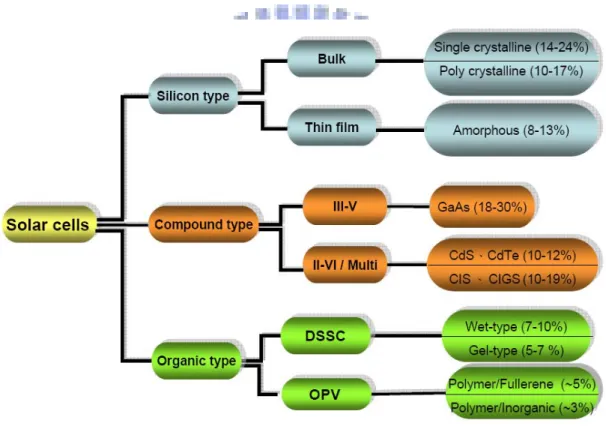
1.1.1 Current status of solar cells
The current status of solar cells is shown in Fig 1-1. The Si single crystalline is the most popular solar cell for our living. The conversion efficiency of Si single
crystalline is up to 24%. However, a dye-sensitized solar cell could possibly offer better efficiency than Si single crystalline. Such a feature of a dye-sensitized solar cell (DSSC) makes it possible for DSSCs to use low- to medium-purity materials through low-cost processes, and provides commercially realistic energy-conversion efficiency. In addition, it is of great importance that the materials used in DSSCs are eco-friendly.
Fig. 1-1 Current status of solar cells
1.1.2 Working principle of DSSC
In 1991, dye-sensitized nanocrystalline TiO2 solar cells (DSSCs) based on the
mechanism of a fast regenerative photoelectrochemical process were first reported by Grätzel et al [1]. The working principle of DSSC is shown in Fig. 1-2. When the
solar cell was excited by incoming light, the original state of the dye is restored by electron donation from the electrolyte, which is usually an organic solvent containing iodide/triioide redox system. The electrons poured into the conduction band of the nanocrystalline TiO2 will eventually reach the anode. The electrons reach the
cathode through the load, where they were then absorbed through redox reaction into electrolytic liquid.
1.2 Motivation
How to produce solar cell at reduced cost has become a critical challenge. Some new ideas for solar-to-electric energy conversion have challenged the traditional devices based on the p-n junction diode for several years [2]. The efficiencies of the TiO2 nanoparticle-based DSSCs has exceeded 10% [3]. A very
important feature of DSSCs is its photoelectrode, which includes mesoporous wide-bandgap oxide semiconductor films with an enormous internal surface area, typically a thousand times larger than that of bulk films. To date, the highest solar-to-electric conversion efficiency has been achieved with films that consist of 20 nm TiO2 nanocrystallites sensitized by ruthenium-based dyes. It is advantageous to
replace the TiO2 nanoparticles with dense array of wide-band-gap semiconductor
nanowires. The morphology of nanowires provides direct conduction paths for the electrons from the dye to the electrode [4]. The semiconductor ZnO has wide gap (3.37 eV) which is similar to TiO2 and very high electron mobility which is about 155
cm2V–1 s–1 for high quality thin film. The ZnO material has a very high UV
emission efficiency at room temperature (free exciton binding energy is 60 meV). It is possible that ZnO may be a new material to construct dye sensitized solar cell [5].
However, to significantly improve energy conversion efficiency of DSSCs remains a challenge. In order to increase efficiency of the nanowire cell, higher dye
loading could be achieved by increasing surface area. Competition between generation and recombination of photoexcited carriers in DSSCs is a technical bottleneck for developing higher conversion efficiency. We are now extending our synthetic strategy to design nanowire electrodes with much larger areas available for dye adsorption.
A solution is to incorporate nanoparticles with original one-dimensional nanostructures [6][7]. The nanowires/nanoparticles composite is mainly ascribed to enrich the light harvesting without sacrificing the electron transport efficiency. Even so, the excess electron hopping through the interparticle barriers still has the chance for charge recombination.
In the present work, we suggested the tree-like ZnO nanowire structures (one-dimensional branches directly attached the main nanowire backbone) could simultaneously afford a direct conduction pathway and achieve higher dye adsorption, therefore significantly enhance the overall efficiency of the DSSC.
The resulting high temperature of fabricating 1-D ZnO nanostructures by the vapor-liquid-solid (VLS) method would create too much resistance within the substrate. Therefore, the aqueous solution method will be first adopted to fabricate ZnO nanowires. Second, the tree-like ZnO nanowire structure was suggested, such that it could afford a direct conduction pathway and could simultaneously achieve
higher dye adsorption. As a result, the overall efficiency of the DSSC was enhanced significantly. It was a considerable success to improve the original conversion efficiency from 0.18% by VLS method up to 1.5% with the tree-like ZnO nanowire structures by chemical bath method.
1.3 Organization of thesis
After the introduction, the thesis includes four other chapters. Chapter 2 discusses the theoretical background of the experiments such as the vapor-liquid-solid method and the chemical bath process, the device operation principles, the electrochemical impedance spectroscopy theory (EIS), and the scanning electron microscopy (SEM), respectively. In Chapter 3, the experimental processes including VLS and solution-liquid-solid (SLS) methods are explored. In Chapter 4, the morphology of ZnO nanowires and I-V curve, EIS, and Photon to Current conversion Efficiency (IPCE) will be investigated. Finally, the final chapter discusses potential future development and concludes the thesis.
Chapter 2 Theoretical background
2.1 Growth mechanism of one-dimensional ZnO nanostructures 2.1.1 Growth Mechanism of Vapor-Liquid-Solid (VLS)
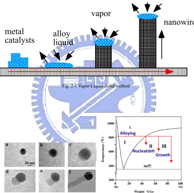
Most popular approach for forming 1-D nanostructures is the vapor-liquid-solid (VLS) method [8]. The VLS method was originally developed by Wagner and his co-workers to produce micrometer-sized whisker in 1960s [9]. Recently, this technique is re-examined by Lieber [8]. In the VLS method, the catalyst plays a key role on the growth of the nanowires or nanorods. The catalyst would form an alloy nanocluster with the reactant under the proper conditions. The growth of the nanowires results from the alloy nanoclusters are supersaturated in the reactant. The formation procedure of 1-D nanostructure in the VLS method is shown in Fig. 2-1, which demonstrates the formation of semiconductor nanowire using metal catalyst. The reactant metal vapor which could be generated by the thermal evaporation is condensed to the catalyst metal to form a liquid alloy nanocluster as the temperature is low. Nanowires grown after the liquid metal alloys become supersaturated and continue as long as the metal nanoclusters remain in a liquid state. Growth of nanowires will be terminated as the temperature reduces to the point that the metal nanoclusters solidify. Therefore, a strong evidence of the VLS mechanism is to
observe catalytic metal at the ends of the nanowires as that observed on the formation of Ge nanowires in the report by P. Yang et al. [10], as shown in Fig. 2-2. Based on the VLS growth mechanism, ZnO nanowires had been successfully grown on silicon substrates also by P. Yang et al. [11].
metal
catalysts
alloy
liquid
vapor
nanowire
Fig. 2-1 Vapor-Liquid-Solid method
Alloying NucleationII
Growth h III
I
Fig. 2-2 In situ TEM images recorded during the process of nanowire growth. (a) Au nanoclusters in solid state at 500 C; (b) Alloying is initiated at 800 oC, at this stage Au exists mostly in solid state; (c) liquid Au/Ge alloy; (d) the nucleation of a Ge nanocrystal on the alloy surface; (e) Ge nanocrystal elongates with further Ge condensation; (f) eventually forms a wire; and (g) Au-Ge binary phase diagram. [11]
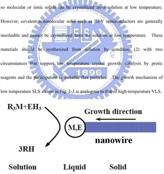
2.1.2 Growth Mechanism of Solution-Liquid-Solid (SLS)
In the SLS growth mechanism [12], crystal growth requires (1) a reversible pathway between the fluid (solution, melt or vapor) and the solid phase or (2) high surface mobility in the solid phase. These conditions let the atoms, ions, or molecules to get the correct positions developing the crystal lattices. Aqueous or organic solvants dissolve their constituent ions or molecules and condition (1) is met, so molecular or ionic solids can be crystallized from solution at low temperature. However, covalent nonmolecular solid such as III-V semiconductors are generally insoluable and cannot be crystallized from the solution at low temperature. These materials should be synthesized from solution by condition (2) with two circumstances that support low temperature crystal growth: catalysis by protic reagents and the participation of metallic flux particles. The growth mechanism of low temperature SLS shown in Fig. 2-3 is analogous to that of high-temperature VLS.
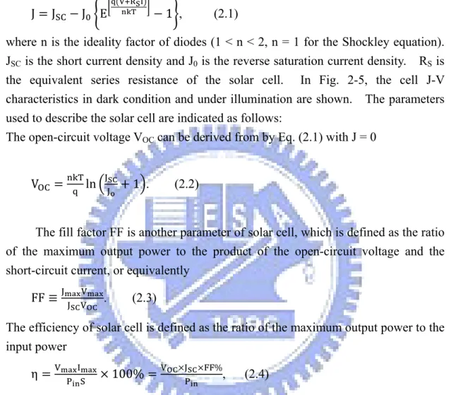
2.2 Device operation principles
Figure 2-4 illustrates the equivalent circuit of an ideal solar cell. From this diagram, one could find the photo-generated current density J can be written as:
J JSC J E
V RSI
T 1 , (2.1)
where n is the ideality factor of diodes (1 < n < 2, n = 1 for the Shockley equation). JSC is the short current density and J0 is the reverse saturation current density. RS is
the equivalent series resistance of the solar cell. In Fig. 2-5, the cell J-V characteristics in dark condition and under illumination are shown. The parameters used to describe the solar cell are indicated as follows:
The open-circuit voltage VOC can be derived from by Eq. (2.1) with J = 0
VOC Tln JSC
J 1 . (2.2)
The fill factor FF is another parameter of solar cell, which is defined as the ratio of the maximum output power to the product of the open-circuit voltage and the short-circuit current, or equivalently
FF JJ V
SCVOC . (2.3)
The efficiency of solar cell is defined as the ratio of the maximum output power to the input power
η V P SI 100% VOC JSC FF%
P , (2.4)
where Pin and S are the input power per unit area and the effective area of solar cell,
Fig. 2-4 Equivalent circuit of an ideal solar cell
2.3 Scanning Electron Microscope (SEM)
The principle of SEM used for examining a solid specimen in the emissive mode is closely comparable to that of a closed circuit TV system shown in Fig. 2-6. In the TV camera, light emitted from an object forms an image on a special screen, and the signal from the screen depends on the intensity of image at the point being scanned. The signal is used to modulate the brightness of a cathode ray tube (CRT) display, and the original image is faithfully reproduced if (a) the camera and display raster are geometrically similar and exactly in time and (b) the time for signal collection and processing is short compared with the time for the scan moving from one picture point to the next.
In the SEM the object itself is scanned with the electron beam and the electrons emitted from the surface are collected and amplified to form the video signal. The emission varies from point to point on the specimen surface, and so an image is obtained. Many different specimen properties cause variations in electron emission, thus, although information might be obtained about all these properties, the images need interpreting with care. The resolving power of the instrument can not be smaller than the diameter of the electron probe scanning across the specimen surface, and a small probe is obtained by the demagnification of the image of an electron source by means of electron lenses. The lenses are probe forming rather than image
forming, and the magnification of the SEM image is determined by the ratio of the sizes of raster scanned on the specimen surface and on the display screen.
For example, if the image on the CRT screen is 100 mm across, magnifications of 100X and 10000X are obtained by scanning areas on the specimen surface 1mm and 10μm across, respectively. One consequence is that high magnifications are easy to obtain with the SEM, while very low magnifications are difficult. This is because large angle deflections are required which imply wide bore scan coils and other problem parts, and it is more difficult to maintain scan linearity, spot focus and efficient electron collection at the extremes of the scan.
(a) (b)
Fig.2-6 Closed circuit TV (a) and scanning electron microscope (b) [13]
2.4 The electrochemical impedance spectroscopy theory in dye-sensitized solar cells
2.4.1 The Bisquert Equation [14]
Bisquert obtained the impedance of diffusion and recombination based on the following three assumptions: (1) electrons in the conduction band diffuse, (2) there is
no trap, and (3) an irreversible first-order reaction is assumed for the recombination. The diffusion-recombination model for small amplitude oscillating quantities, superimposed to a given stationary state, is written as
J kn D kn, (2.5)
where n , D, and k represent the small oscillating electron density, diffusion coefficient of an electron in the ZnO nanocrystal, and reaction rate constant for recombination, respectively.
The boundary condition is given as
0, at x L, (2.6)
where L represents the film thickness of ZnO. The impedance under boundary condition (2) is given by Bisquert as
Z RWRK coth 1 , (2.7)
where
ω LD , ω k , (2.8) R ConDL, Con BT
A , R R ConL , (2.9)
Here, Z, Rw, Rk, τ, kB, T, q, A, and ns represent the impedance, electron transport
resistance in TiO2, charge-transfer resistance related to recombination of an electron,
lifetime of an electron in ZnO, Boltzmann constant, absolute temperature, charge of a proton, the electrode area, and the electron density at the steady state in the
conduction band, respectively.
Equation (2.7) can be rewritten to obtain
Z R coth 1 . (2.10)
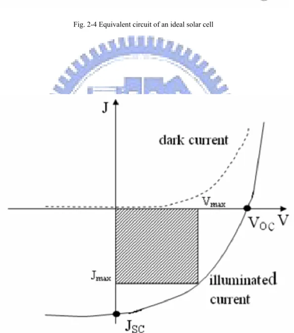
Fig. 2-7 Reaction paths in the TiO2 electrode of the DSSCs in the model of Kern et al.[15]
On the other hand, Kern et al. [15] derived the impedance of diffusion and recombination in TiO2 based on the reaction paths shown in Figure 2-7. They set the
following three assumptions:
injection rate G under illumination; (2) only a single trap level is assumed, and the rate constant, k1, for the trapping of the conduction band electrons is much faster than
k2 for the detrapping of the electrons; and (3) trapped electrons are lost by the
recombination with I3-, and the second-order reaction rate is assumed with respect to
electrons for the recombination.
The continuity equations for the conduction band electrons and for the electrons in the trap state, which describes injection, diffusion, collection, trapping, detrapping, and recombination of electrons in the TiO2 of the DSSCs, are given as
D k n k N G, (2.11)
N k n k N k n, (2.12)
n n ∆ne , (2.13) N N ∆Ne , (2.14)
where Dcb represents the diffusion coefficient of an electron in the conduction band
and ns and Ns are the steady state electron density in the conduction band and in the
trap state, respectively. ∆n and ∆N are the amplitudes of the modulated component of the conduction band and trap state electron density, respectively.
Defining
D D , (2.15) Dk 2NSk , (2.16)
γ D D . (2.17)
And using the following boundary conditions At x=L, qD ∆ ∆IA ∆J; (2.18) At x=0, ∆ 0. (2.19)
Impedance is obtained by Kern et al. [15] as Z S A D L L, (2.20) where S BT S . (2.21)
Equation (2.16) was transformed into Eq. (2.20) as follows. Defining
ω DL , ω k , (2.22) γL , (2.23) and impedance can be rewritten as
Z R coth 1 , (2.24) where R BT A L D Con L D , R ConL . (2.25)
Then, Eq. (2.24) becomes the same as Eq. (2.10)
Let us consider here the reason why the impedance by Kernet al. becomes the same as the Bisquert equation. The assumption that the trapping is much faster than
detrapping (k1 » k2) results in Ns » ns. Electrons in the trap state N detrap to the
conduction band and diffuse with the diffusion coefficient Dcb for the period
proportional to k2/k1. Thus, electrons in the trap state are regarded as diffusing
charges with the diffusion constant Deff = Dcb(k2/k1). Electrons in the trap state also
react with I3- with a pseudo-first-order reaction rate with reaction rate constant keff
=2Nskr. Therefore, the model by Kern et al. is simplified as follows:
Injected electrons become the trap electrons, diffusing with the diffusion coefficient
Deff and being lost by the pseudo-first-order recombination rate with the rate constant
keff. This reaction scheme is eventually the same as that of Bisquert.
2.4.2 Models of the Impedance of the Electron Transfer at the Pt Counter Electrode and the Finite Warburg Impedance of Tri-Iodide in Electrolyte
First, the impedance of the electron transfer at the Pt counter electrode can be described approximately by the following simple RC circuit with
Z
C , (2.26)
ω C , (2.27)
where rp and Cp represent the resistance at the Pt surface and the capacitance at the Pt
surface, respectively.
Second, the finite Warburg impedance describes the diffusion of triiodide ions in the electrolyte as
ZN RD DI tanh DI, (2.28) R BT DI D A VC , (2.29) ω 2.5DI, (2.30)
where Dl and δ represent the diffusion coefficient of I3 – and the thickness of the
liquid film, respectively. The number of electrons transferred in each reaction, m, is 2 in this case. AV and C* are Avogadro’s constant and the concentration of I3- in the
bulk, respectively.
2.4.4 The total impedance of the DSSC
The total impedance of the DSSC, ZS, is given as the summation of the
impedance of diffusion and recombination in the ZnO electrode, Z, given by Eq. (2.24), Z , given by Eq. (2.25??), and Zp N, given by Eq. (2.27??), and
ZS Z ZP ZN. (2.31)
2.5 IPCE Measurements
The incident-photon-to-current-efficiency (IPCE), also referred to as incident-photon-to-collected-electron-efficiency, gives the spectral resolution of the photocurrent. These measurements were done in Ar-glove boxes using a homemade setup: The light coming from a Xe-lamp is optically chopped. After passing a monochromator the light is focused onto the sample using a light fibre. Each time
the lamp is turned on, the lamp spectrum is calibrated using a monocrystalline silicon diode with known sensitivity. For signal detection a lock-in amplifier is used. After the measurement the IPCE can be calculated using
IPCE % 1240 V nm I AI W 100%. (2.32) In this equation Ip is the light power incident on the device.
Chapter 3 Experiment and measurement
3.1 Sample preparation 3.1.1 VLS method
The ZnO nanowires were grown by thermal vapor deposition from zinc vapor and a little oxygen gas on FTO (F:SnO2) conducting glass substrate, which has wire
resistance of 10 Ω/cm2. The vertical distance between the metal source and the
sample was about 3~5 mm. Then the alumina boat which carried the substrate was inserted into a quartz tube. This quartz tube was placed inside a furnace, with the center of the alumina boat positioned at the center of the furnace and the substrates placed downstream of growth metal powder (Fig. 3-1). The quartz tube was evacuated to a pressure below 2 x10⁻² torr using mechanical pump. After the
high-purity argon gas was infused into the system with a flow rate of 500 sccm and pressure controlled at 10 torr. The zinc vapor was transported with argon carrier gas with controllable flow rate ranging from 500 sccm to 700 sccm, and pressure ranging 10torr to 30 torr, to change the rods’ length.
Fig. 3-1 Thermal vapor transport system
3.1.2 SLS method
First, the arrays of ZnO nanowires were synthesized on seeded fluorine doped tin oxide (FTO) substrates (3 mm thickness, 10 Ω per square, Nippon Sheet Glass) similar to P. D. Yang et al. by immersing the seeded substrates in aqueous solutions containing 0.08 M zinc nitrate hydrate (98%, Riedel-deHaën), 0.08 M hexamethylenetetramine (99%, Showa), and 12 mM polyethylenimine (branched, low molecular weight, Aldrich) at 95 °C for 10 hours. Second, in order to fabricate the branched nanowires, the ZnO nanowires substrate obtained from the first step were re-coated with ZnO seed layer by dip-coating in a 0.005 M zinc acetate dihydrate (99%, Riedel-deHaën) in ethanol. Then the branched nanowires were grown by immersing the seeded ZnO nanowires in aqueous solutions containing 0.02 M zinc nitrate hydrate, 0.02 M hexamethylenetetramine and 3 mM polyethylenimine at 95 °C
for 5 hours. The branched ZnO nanowires were finally rinsed with deionized water and baked in air at 450 °C for 30 minutes to remove any residual organics. The growth procedure was illustrated in Fig. 3-2
Fig. 3-2 The schematic growth procedure from the original ZnO nanowires to the branched ZnO
nanowires.
3.2 Fabricate the DSSCs
Dye-sensitized solar cells were prepared by immersing the branched ZnO nanowires on substrates into a solution of 0.5 mM cis-bis(isothiocyanato)bis(2,2’-bipyridyl-4,4’-dicarboxylato)-ruthenium(II)
bis-tetrabutylammonium (N719, Solaronix) in acetonitrile/tert-butanol (1:1) for 15 mins, and the films were then rinsed with acetonitrile. The sensitized electrodes were sandwiched together with thermally platinized FTO counter electrodes separated by 25-μm-thick hot-melt spacers (Surlyn, Dupont). The internal space of the cell was filled with an electrolyte solution (0.1M LiI, 0.5M 1,2-dimethyl-3-propylimidazolium iodide, 0.03M I2, and 0.5M tert-butylpyridine in
3.3 Scanning Electron Microscope (SEM) system
The morphology of ZnO-based nanostructures was observed by the Field Emission Gun Scanning Electron Microscopy (FEG-SEM) [JEOL JSM-6500F]. The accelerated voltage is 0.5-30kV and the magnification is 20-300k times, as shown in Fig. 3-3.
3.4 The equipments of conversion efficiency measurement and impedance spectroscopy
Efficiencies for solar energy conversion and ac impedance spectroscopy were immediately evaluated under AM 1.5G simulated sunlight (Yamashita Denso, YSS-100A) and electrochemical analyzer (Autolab, PGSTAT3). The light power was calibrated with a set of neutral density filters by using a silicon photodiode (BS-520, Bunko Keiki).
Chapter 4 Results and Discussion
4.1 ZnO nanowire based dye-sensitized solar cell manufactured by VLS 4.1.1 Growth of ZnO nanowires with VLS
The images shown in Fig. 4-1 are the SEM cross-sectional views of the nanostructures. Figure 4-1(a) shows the ZnO film and Fig. 4-1(b) shows the ZnO rods grown at 550 ℃ under 10 torr tube pressure with 500 sccm of flow rate for 60 mins. Their lengths are about ~ 2 μm. Figure 4-1(c) shows the rods grown at 550 ℃ under 100 torr tube pressure with 700 sccm of flow rate for 60 mins. Their lengths are about ~ 4 μm.
(a)
(b)
(c)
4.1.2 The energy conversion of DSSCs base on ZnO nanowires grown by VLS
The current-voltage characteristics for a solar cell constructed using nanowires with Pin = 100 mW/cm2 broadband illumination were shown in Fig. 4-2. Active
electrode area was typically 0.2827 cm2. Figures 4-2(a) and (b) show the I-V curve
with the incident light came from the top and the bottom of the solar cell, respectively. Because the incident light has to pass through the translucent ZnO buffer layer, less of the absorbed energy of incidence by the dye on the nanowires and so the Jsc for which
the light came from the bottom of the solar cell is less than that the light came from the top of the solar cell. The relations of the short circuit current, the open circuit voltage, the fill factor, and the overall efficiency to length of nanowires are shown in Table 1. Obviously, the solar cell with longer nanowires has the better conversion efficiency, and the worst conversion efficiency obtained for using the ZnO film. It can be interpreted as the larger surface area can adsorb the more dye for the longer ZnO nanowires. The external quantum efficiency (ECE), which is the percentage of electrons collected per incident photon (with no correction for reflection losses), will increase as increasing length [16].
Additionally, after having been grown the ZnO nanowires by thermal vapor deposition at 550oC for an hour, the resistance of the FTO conducting glass substrates
0.05, 0.3, and 0.4 V in Fig. 4-2 for the films of ~2 μm, and ~4 μm thick. The higher sheet resistance reduces short-circuit current which causes the lower conversion efficiency as compared with the reported results [17, 18] of the ZnO nanowire-based dye-sensitized solar cell.
sample Film 2μm 4μm η(%) 0.09 0.15 0.18 Voc (V) 0.73 0.75 0.73
Jsc (mA/cm2) 0.19 0.45 0.62
FF 0.65 0.44 0.40
Table 1 The short circuit current, the open circuit voltage, the fill factor, and the overall efficiency of the solar cell with different lengths of nanowires.
0.0 0.1 0.2 0.3 0.4 0.5 0.6 0.7 J(mA /c m 2 ) film ~ 2 µm ~ 4 µm
(a)
0.0 0.1 0.2 0.3 0.4 0.5 0.6 0.7 0.00 0.05 0.10 0.15 0.20 0.25 0.30 J(mA/cm 2 ) E(V) film ~ 2 µm ~ 4 µm
(b)
Fig. 4-2 Current-voltage characteristic of a ZnO nanowire-based dye sensitizes solar cell with 100
mW/cm2 broadband visible illumination.(a)the incident light came from the top of the solar cell and
(b)the incident light came from the bottom of the solar cell.
4.2 ZnO nanowire based dye-sensitized solar cell manufactured by SLS
The arrays of ZnO nanowires were synthesized on seeded fluorine doped tin oxide (FTO) substrates (3 mm thickness, 10 Ω per square, Nippon Sheet Glass) by immersing the seeded substrates in aqueous solutions containing 0.04 M zinc nitrate hydrate (98%, Riedel-deHaën), 0.04 M hexamethylenetetramine (99%, Showa) and at 75 °C for 8 hours. The image shown in Fig. 4-3 is the SEM cross-sectional view of the nanowires. The efficiency of the DSSC made by this nanowires sample is about
0.153 at % and the I-V curve is shown in Fig. 4-4. Active electrode area was typically 0.2827 cm2. The short circuit current density, the open circuit voltage, the
fill factor are 0.905mA/cm2, 0.67V and 0.252, respectively and are summarized in
Table 4-2. As compared with the report of P. D. Yang, et al. [17], it still has a lot to improve in efficiency. The I-V curve indicates not only there is a large barrier between nanowires and FTO but also the nanowires with length of ~1 μm and diameter of 100 nm may not offer sufficient surface area for dye to stick on.
Fig. 4-3 The SEM images of the ZnO rods fabricated by SLS with 0.04 M zinc nitrate hydrate (98%,
Fig. 4-4 The I-V curve of the ZnO rods fabricated by SLS with 0.04 M zinc nitrate hydrate (98%,
Riedel-deHaën), 0.04 M hexamethylenetetramine (99%, Showa) and at 75 °C for 8 hours.
η(%) Voc (V) Jsc (mA/cm2) FF
0.153 0.666 0.905 0.252
Table 4-2 The short circuit current, the open circuit voltage, the fill factor, and the overall efficiency of
the solar cell, in which the nanowires were manufactured by SLS with 0.4M nitrate hydrate, etc.
0.0 0.2 0.4 0.6 0.8 0.0 0.1 0.2 0.3 0.4 0.5 0.6 0.7 0.8 0.9 1.0 1.1 (0.666,0) Cur re n t den s it y(mA /cm 2 ) Voltage(V) Fill Factor:0.252403109 Efficiency:0.153413647% (0.4,0.383) (0,0.905)
4.3 Ultra long nanowires to improve the efficiency of the DSSCs manufactured by SLS
The process of the growth of the ZnO nanowires is also the same as that mentioned in Section 4.2, but some different steps were used, e.g., 0.6 M zinc nitrate hydrate (98%, Riedel-deHaën), 0.06 M hexamethylenetetramine (99%, Showa) and 12 mM polyethylenimine (branched, low molecular weight, Aldrich) and stirred at 95 °C for 2.5 hours three times. The image shown in Fig. 4-5 is the SEM cross-sectional view of the nanowires. It seems that the length of nanowies are much longer than those mentioned in the previous section. The function of the polyethylenimine and repeating grown for three times at 95 °C is to make high aspect ratio nanowires.
The relations of the short circuit current, the open circuit voltage, the fill factor, and overall efficiency to length of nanowires were also listed in Table 4.3. Active electrode area was typically 0.2827 cm2. J
SC and the fill factor become 2.82 mA/cm2
and 0.44. So the efficiency is higher than that mentioned in Section 4.2. The longer nanowires offer more surface area for dye adsorption and so have the higher efficiency. In the next chapter we will use another process to improve the efficiency of DSSCs.
(a)
(b)
(c)
Fig. 4-5 The SEM images of the ZnO rods (a) without PEI, (b) with PEI, and (c) with PEI and grow 3
Fig. 4-6 The I-V curve of the ZnO rods fabricated by SLS with 0.06 M zinc nitrate hydrate (98%,
Riedel-deHaën), 0.06 M hexamethylenetetramine (99%, Showa) and 12 mM PEI and at 95 °C for 2.5
hours three times.
Table 4-3 The short circuit current, the open circuit voltage, the fill factor, and the overall efficiency of
4.4 Tree-like ZnO nanowries
Using the process described in section 3.1.2, we obtained slightly off-aligned seeded ZnO nanowires with density of about 7x108 cm-2 grown on the FTO substrate,
as shown in Fig. 4-7. It shows the seeded ZnO nanowires were formed of little crystalline nanopaticles with diameter 10-20 nm attached to the backbone bare nanowires having length and diameter in the range of 7-8 µm and 150–250 nm, respectively. After the second growth step, the radial secondary branches emanated from the seeds, as shown in Figs. 4-7(b) and (c).
Fig. 4-7 Before (a) and After (b) re-coating a seed layer of the original ZnO nanowires obtained from
aqueous solution. (c) Low- and (d) High-magnification images of the branched ZnO nanowires after
The secondary branches or branched nanowires have length and diameter ranging from 100-300 nm and 20-50 nm, respectively. Although the branched nanowires have non-uniform size due to the roughly dip-coating process, they still can offer more sufficient internal surface area for dye adsorption as compared with the bare nanowires.
The photocurrent–voltage (J-V) characteristics for solar cells constructed using ZnO nanostructures with 100 mW/cm2 broadband illumination from a xenon lamp
were shown in Fig. 4-8. Active electrode area was typically 0.2827 cm2. Table 4.4
summarizes the measured and the calculated values obtained from each J-V curve. The short-circuit current density (Jsc) and the overall light conversion efficiency of the
branched ZnO nanowires are 2.37 mA/cm2 and 1.51 %, respectively, and almost twice
higher than that of the bare ZnO nanowires. One factor for the increase in short-circuit current density is the enhanced photon absorption associated with the presence of enlargement of internal surface area resulting in sufficient dye-loading. Although the length and density of ZnO structures exhibit the disadvantage compared with previous study [19], the overall efficiency can achieve almost the same value via utilizing the extra secondary nanobranches. The values of fill factor (FF) for ZnO DSSCs are general lower than those using TiO2 nanoparticles (0.6–0.7). This is
tri-iodide ions in the electrolyte. Slightly different value in the bare ZnO nanowire and branched ZnO nanowire DSSCs reveal the almost same interfacial recombination, which is evidenced by the equivalent value of the shunt resistance Rsh=(dV/dI)V=0
from the I-V curves under illumination. The series resistance Rs=(dV/ dI)I=0 for
branched ZnO nanowire DSSC (25.64 Ωcm2) is significantly lower than the bare ZnO
one (46.13 Ωcm2) and is previously explained association with the dye loading but not
the nanowire length [20].
0.0 0.2 0.4 0.6 0.8 -5 -4 -3 -2 -1 0 1 2 3 4 5
C
u
rren
t den
si
ty (m
A
/cm
2)
Voltage (V)
ZnO NWs (dark) ZnO NWs (100 mW/cm2 )Branched ZnO NWs (dark) Branched ZnO NWs (100 mW/cm2
))
Fig. 4-8 Current density against voltage (J-V) characteristics
Recently, electrochemical impedance spectroscopy (EIS) measurement has been widely performed to investigate electronic and ionic processes in dye-sensitized solar
cells [21, 22, 23, 24, 25]. The Nyquist plots of the impedance data for bare and branched ZnO nanowire DSSCs were performed by applying a 10 mV ac signal over the frequency range of 10−2–105 Hz under illumination at the applied bias of V
oc, as
shown in Fig. 4-9(b). Some interior parameters of the devices with thickness of LF
can be derived by well fitting the impedance data of the Nyquist plots to expressions based on the equivalent circuit of nanowire DSSC suggested by Wu et al [23, 24].
Although the concrete equivalent circuit may be more complex than the previous reports. According to the formation of Zn2+/dye complexes from the dissolution of
surface Zn atoms in the acid dye system and finally block the electron transport from the dye to semiconductor [26]. Hence, the impedance data obtained at different applied potentials cannot be fitted with a single equivalent circuit and some components such as an inductor element should be considered [27]. In order to avoid the unnecessary interference from the trapped electrons, we presently ignored the low frequency part of impedance data. The fitted results were also listed in Table 4.4, which includes the first-order reaction rate constant for the loss of electrons (keff),
the electron lifetime (τ=1/keff), the electron transport resistance (Rw), and the charge
transfer resistance related to recombination of electron at the ZnO/electrolyte interface (Rk). We found Rk and Rw are quite similar for both DSSCs in this present work,
bare ZnO nanowires or branched ZnO nanostructures. On the contrary, keff in the
branched ZnO nanowire DSSC is smaller than the bare nanowire one to cause the smaller effective diffusion length [22] (Deff = (Rk/Rw)LF2keff ) in branched ZnO
nanowire DSSC. Since keff is related to reaction rate, the electron lifetime, τ = 1/keff,
could be prolonged by the additional transport distance between branches and conductive electrode (backbone nanowire).
0 20 40 60 80 100 120 140 0 10 20 30 40 50 60 Z '' ( Ω ) Z'' (Ω) - ZnO NWs - Branched ZnO NWs
Fig. 4-9 Nyquist plots of the bare ZnO nanowires and branched ZnO nanowires DSSCs under AM1.5
In general, the current density for a DSSC is determined by the initial number of photogenerated carriers, the electron injection efficiency from dye molecules to semiconductor, and the recombination rate between the injected electrons and oxidized dye or redox species in the electrolyte. Base on the assumption of the same injection efficiency and recombination rate for the given ZnO DSSC systems, it is reasonable that the initial number of photogenerated carriers may be significantly affected by the variation in the light-harvesting capability of different-structured photoanodes. Figure 4-10 displays the wavelength distribution of incident monochromatic photon to current conversion efficiency (IPCE). The photocurrent peaks occurring at approximately 400 nm are due to direct light harvesting by ZnO semiconductor (see Fig. 4-11), in which the photogenerated electrons diffuse through ZnO and the holes in the valence band are replenished directly by charge transfer from the I3-/I-electrolyte [20]. The maxima of IPCE in the visible region contributed
by the dye absorption are located at approximately 525 nm (see Fig. 4-12), corresponding to the visible t2Æπ* metal-to-ligand charge transfer (MLCT). The
IPCE obtained for the branched ZnO nanowire DSSC is almost 1.5 times that of the bare ZnO nanowire. The improvement in the IPCE suggests that the high energy conversion efficiency results predominantly from sufficient dye-loading by branched ZnO nanowires, which enlarge internal surface area within the photoelectrode. This
concept is anticipated to be equally applicable to other semiconductor photoelectrodes in DSSCs and organic–inorganic hybrid solar cells, despite that the filling factor of the ZnO nanostructures are not optimized at this point, as previously shown in the SEM images (see Fig. 4-7). Further improvement of energy conversion efficiency could be implemented through adjusting denser and longer branches to fill the interstitial voids between backbone nanowires, which will substantially improve the light harvesting and the current density.
400 450 500 550 600 650 700 0 5 10 15 20 25 30
IP
C
E
(
%
)
Wavelength (nm)
Branched ZnO NWs ZnO NWsFig. 4-10 The incident monochromatic photon to current conversion efficiency (IPCE) of the bare
Fig. 4-11 The photoluminescence spectra of ZnO under 325 nm He-Cd Laser excitation.
Chapter 5 Conclusion and Future Works
5.1 Conclusion
High growth temperature which uses the vapor-liquid-solid (VLS) method creates too much resistance in the substrate. The resistance of FTO changes from 10 Ω per square to 150 Ω per square. Nevertheless, using the aqueous solution method to fabricate ZnO nanowires has successfully solved this problem. The length of the nanowires is related to conversion efficiency. We can use different concentration of zinc nitrate hydrate and PEI to manipulate the length of nanowires. The branched ZnO nanowires have been fabricated on FTO substrates using aqueous solution re-buffer method for dye sensitized solar cells. The short-circuit current density and the overall light conversion efficiency of the branched ZnO nanowire DSSC nearly doubled the bare ZnO nanowire. The improvement can be explained in association with the enlargement of internal surface area within the photoelectrode without increasing interparticle hops. In addition, the sufficient dye-loading in branched ZnO nanowire DSSC was further evidenced from the lower series resistance Rs=(dV/
dI)I=0 and significantly enhanced IPCE spectra than the bare ZnO nanowire one.
Therefore, the concept of these one-dimensional branched nanostructures could significantly enhances the overall energy conversion efficiency of the DSSC.
5.2 Future works
We found that nanobranches only appear on the tops of ZnO nanowires. If the branches were all around the nanowires, the short circuit current should overtake 2%. First, SLS could be used to grow trunks of the nanotrees. Second, we can re-buffer by atomic layer deposition method (ALD). ALD can manufacture multi-crystal ZnO thin film uniformly on the surface of ZnO nanowires. Then the first process could be repeated to grow the branches.
We also have an idea that Mercurochrome may replace N719. Mercurochrome has higher diffusion length with nanowires. The diffusion length of our nanotree DSSC has not yet optimized. Mercurochrome may solve this problem and improve the conversion efficiency. Table 5-1 shows Deff of Mercurochrome is higher than
that of N3.
Table 5-1 the parameter of DSSC with Mercurochrome and the parameter of DSSC with N3. [7]
Figure 5-1 shows the band gap difference between ZnO and TiO2. If one can
tune the band gap of ZnO based matrerials closer to the band gap of TiO2, the
conversion efficiency of ZnO DSSC has the chance to exceeded 10%. Mg doped ZnO can vary the band gap from 3.3 eV to 4.0 eV with increasing Mg content [29],
although, there is still a big challenge to manufacture MZO nanowires by low temperature method.
References
[1] B. Oregan and M. Grätzel, Nature 353, p. 737 (1991). [2] M. Grätzel, Inorg. Chem. 44, 6841 (2005).
[3] M. K. Nazeeruddin, F. DeAngelis, S. Fantacci, A. Selloni, G. Viscardi,P. Liska, S. Ito, B. Takeru, and M. Grätzel, J. Am. Chem. Soc. 127, 16835 (2005).
[4] K. Keis, E. Magnusson, H. Lindstrom, S. E. Lindquist, and A. Hagfeldt, Sol. Energy Mater. Sol. Cells 73, 51 (2002).
[5] T. Stergiopoulos, I. M. Arabatzis, H. Cachet, and P. Falaras, J. Photochem. Photobiol. A 155, 163 (2003).
[6] B. Tan and Y. Wu, J. Phys. Chem. B 110, 15932 (2006). [7] C. H. Ku and J. J. Wu, Appl. Phys. Lett. 91, 093117 (2007). [8] Morales AM, and Lieber CM, Science, 279,208 (1998). [9] R. S. Wagner, and W. C. Ellis, Appl. Phys. Lett., 4, 89(1964). [10] Y. Wu and P. Yang, J. Acm. Chem. Soc, 123, 3165 (2001).
[11] M. H. Huang, Y. Wu, H. Feick, N.Tran, E. Weber, and P. Yang, Adv. Mater. ,13 , 113, (2001)
[13] A scanning electron microscope comparison of microfilied fixed prosthodon, R. A. Strohaver, Harry G. Armstrong Aerospace Medical Research Laboratory
(1987).
[14] Bisquert, J. J. Phys. Chem. B, 106 (2), 325-333 (2002).
[15] Kern, R.; Sastrawan, R.; Ferber, J.; Stangl, R.; Luther, J. Electrochim.
Acta, 47, 4213-4225 (2002).
[16] W. U. Huynh, J. J. Dittmer, and A. P. Alivisatos, Science 295, 2425(2002) [17] M. Law, L. E. Greene, J. C. Johnson, R. Saykally, and P. D. Yang, Nature
Materials 4 (6): 455-459 (2005).
[18] J. B. Baxter, and E. S. Aydil, Appl. Phys. Lett. 86, 053114(2005).
[19] M. Law, L. E. Greene, J. C. Johnson, R. Saykally, and P. D. Yang, Nat. Mater. 4 455 (2005).
[20] A. D. Pasquier, H. Chen, and Y. Lu, Appl. Phys. Lett. 89, 253513 (2006). [21] Q. Wang, J. E. Moser, and M. Grätzel, J. Phys. Chem. B 109, 14945 (2005). [22] M. Adachi, M. Sakamoto, J. Jiu, Y. Ogata and S. Isoda, J. Phys. Chem. B 110, 13872 (2006).
[23] J. J. Wu, and D. K. P. Wang, Adv. Mater. 19, 2015 (2007).
[24] J. J. Wu, G. R. Chen, H. H. Yang, C. H. Ku, and J. Y. Lai, Appl. Phys. Lett. 90, 213109 (2007).
[25] C. J. Lin, W. Y. Yu, and S. H. Chien, Appl. Phys. Lett. 91, 233120 (2007). [26] H. Horiuchi, R. Katoh, K. Hara, M. Yanagida, S. Murata, H. Arakawa, and M. Tachiya, J. Phys. Chem. B 107, 2570 (2003).
[27] W. C. Chen, T. C. Wen, C. C. Hu, A. Gopalan, Electrochim. Acta 47 1305 (2002). [28] Yanfang Zhang, Huarong Zhang, Yunfei Wang, and W. F. Zhang. J. Phys. Chem. C, 112, 8553–8557 (2008).
[29] Hsu HC, Wu CY, Cheng HM, Hsieh WF, Appl. Phys. Lett. 89, 013101 (2006). [30] A. Arakawa et al. SEMSC. 64, 115 (2000).

![Fig. 1-2 Working principle of DSSC [1]](https://thumb-ap.123doks.com/thumbv2/9libinfo/8247646.171573/13.892.189.715.415.1069/fig-working-principle-of-dssc.webp)
![Fig. 2-7 Reaction paths in the TiO 2 electrode of the DSSCs in the model of Kern et al.[15]](https://thumb-ap.123doks.com/thumbv2/9libinfo/8247646.171573/25.892.150.742.167.848/fig-reaction-paths-tio-electrode-dsscs-model-kern.webp)