利用特殊接觸電極進行橫向擴散元件之特性分析與SPICE模型建立
51
0
0
全文
(2) 利用特殊接觸電極進行橫向擴散元件之 特性分析與 SPICE 模型建立. 學生:熊勖廷 國立交通大學. 指導教授:汪大暉 博士 電子工程學系. 電子研究所. 摘要 在此論文中,將觀察自發熱效應(self-heating effect)所引發的內部電壓(internal voltage)退化現象。我們提出一個具有特殊接觸電極之 LDMOS(橫向兩次擴散之金 氧半場效電晶體)結構,藉以量測高閘極脈波造成之內部電壓暫態變化。接著,我 們將自發熱效應所造成之內部電壓退化與集極電流退化情形作一比較,最後證明 內部電壓是觀察自發熱效應之較好方法。 我們將建立一個具有兩個組成元件之 LDMOS SPICE 模型,此模型也會納入 自發熱效應的模擬。模擬結果準確描述了 LDMOS 在高閘極脈波下集極電流之暫 態變化,顯示我們已成功建立了自發熱模型。在不同閘極和集極偏壓下,有/無自 發熱效應之電流模擬結果,都將在論文中呈現。. i.
(3) Characterization and SPICE Modeling of Lateral Diffused MOS by using a Novel Metal Contact Structure. Student: Hsu-Ting Shiung. Advisor: Dr. Tahui Wang. Department of Electronics Engineering & Institute of Electronics National Chiao Tung University. Abstract. Self-heating induced internal voltage degradation is observed. A novel lateral diffused MOS transistor with an additional metal contact for internal voltage measurement is introduced. An internal voltage transient at high gate voltage pulse is measured. A comparison of self-heating characterization by the internal voltage method and the conventional drain current method is presented. The internal voltage method is demonstrated to be more sensitive than drain current method for self-heating characterization. A two-component VI-based LDMOS SPICE model including self-heating effect is proposed. Our model accurately depicts the LDMOS drain current transient at high gate voltage pulse, demonstrating successful use of the self-heating model. Modeling results of the. ii.
(4) self-heating and non-self-heating currents at various VG and VD are also shown.. iii.
(5) 謝誌 本篇論文完成,首先要感謝我的指導教授汪大暉教授。他嚴謹的研究態度, 讓我獲益良多。也感謝指導我論文,陪我奮鬥到最後一刻的志昌學長,以及實驗 室的小馬學長、DaDa 學長、阿雄學長和阿多肯學長。另外感謝和我同屆的元鵬、 彥君、佑亮、子華,還有學弟妹阿杜和阿標。最重要的,感謝我的父母和家人, 給我精神上和經濟上穩固的支持,幫助我順利完成碩士學業。 2008.6. iv.
(6) Contents i ii iv v vii. Chinese Abstract English Abstract Acknowledgement Contents Figure Captions Chapter 1 Chapter 2 2.1 2.2. 2.3 2.4 2.5. Chapter 3 3.1 3.2. 3.3. 3.4. Chapter 4. Introduction A Novel Metal Contact Structure for Self-Heating and Device Characterization. 1 4. Introduction A Novel Metal Contact Structure for Internal Voltage Measurement 2.2.1 Device Structure 2.2.2 Internal Voltage Transient Comparison of the VI Method and Conventional ID Method Comparison of LDMOS/MOS Characteristics Summary. 4 4. An Internal-Voltage-Based SPICE Model Including Self-Heating Effect Introduction Model Description 3.2.1 Model Components 3.2.2 Model Process Modeling Flow 3.3.1 MOS Parameters Extraction 3.3.2 VI Simulation 3.3.3 VI Model Results and Discussions. Conclusion. 4 5 6 6 7 13 13 14 14 14 15 15 15 16 18 35 36 38. Reference Appendix. iv.
(7) Figure Captions. Fig. 1.1 Organization of thesis. Chapter2 discusses self-heating characterization while chapter3 focuses on SPICE model including self-heating effect. (p.3) Fig. 2.1 (a) Cross-section of a novel LDMOS structure. The metal contact (VI) is arranged in the bird’s beak region with an n+ implant. (b) Transient measurement setup for internal-voltage characterization. (p.8) Fig. 2.2 Transient VI measured at high gate voltage pulse. Self-heating induced VI decrease is observed. (p.9) Fig. 2.3 (a) ID versus VD in SHE (DC Meas.) and SHE-free (Transient Meas.) conditions. At VG/VD=40V/40V, SHE induces 8% change in drain current. (b) VI versus VD in SHE and SHE-free conditions. A 23% change caused by SHE is seen at VG/VD=40V/40V. (p.10) Fig. 2.4 ID versus VI at VG=40V. In the saturation region, a VI change of 23% corresponds to a relatively small change in ID. (p.11) Fig. 2.5 (a) Current versus voltage of the LDMOS (ID-VD) and the intrinsic MOS (ID-VI) in the low-VG region. The I-V of the intrinsic MOS and the LDMOS in linear region and saturation regions are almost identical.. vii.
(8) (b) High-VG current versus voltage of the LDMOS and the intrinsic MOS. A significant current difference is observed in the saturation region. (p.12) Fig. 3.1 (a) Equivalent circuit model of the LDMOS device. The MOS represents the channel region while the VI controller accounts for the drift region. (b) Illustration of different operation regions controlled by each component. (p.20) Fig. 3.2 Process of the VI-based LDMOS model. (p.21) Fig. 3.3 Process of the VI controller. Here self-heating effect is taken into account. (p.22) Fig. 3.4 A specially-designed modeling flow to set up the MOS model and the VI model. Five steps are indicated, including (1) and (2) MOS parameter extraction, (3) VI simulation, (4) VI model, and (5) LDMOS macro model. (p.23) Fig. 3.5 A comparison of measurement data and model fitting results after step 1. (a) Low-VG and (b) High-VG. (p.24) Fig. 3.6 A comparison of measurement data and model fitting results after step 2. (p.25) Fig. 3.7 A special simulation method to obtain internal voltage data from the input drain current. The MOS parameters are extracted from step 1 and 2. Typical VI simulation result is plotted under self-heating (w. SH) and non-self-heating (w/o SH) conditions. (p.26) Fig. 3.8 Model VI equations plotted at VG=20V. Eq.1 represents VI in the linear. viii.
(9) region while Eq.2 depicts saturation VI. Eq.3 is the effective VI for both linear and saturation regions. (p.27) Fig. 3.9 Comparison of the non-self-heating VI simulation data and the VI model built by model equations. (a) VI-VG and (b) VI-VD. (p.28) Fig. 3.10 ID transient and the corresponding simulation VI transient. The SH-induced total VI change β and the time constant τC are extracted from the transient VI. (p.29) Fig. 3.11 RC sub-circuit for modeling of transient VI change. (p.30) Fig. 3.12 Simulation and model ΔVI(t) and VI(t). (p.31) Fig. 3.13 Modeling result of the drain current transient at VG=VD=40V. (p.32) Fig. 3.14 Comparison of measurement and model ID versus VD at (a) Low-VG and (b) High-VG. The model drain current values w/o SHE and w/ SHE are extracted from the model ID transient at t=0 and t=30μs respectively. (p.33) Fig. 3.15 Modeling results of ID versus VG in (a) linear region and (b) saturation region. (p.34). ix.
(10) Chapter 1 Introduction The continuous scaling down of CMOS technology is accompanied by the reduction of the power supply voltages. Power MOSFETs, with their high-voltage capabilities, were first introduced in the 1970s [1] to enable low-voltage integrated circuits to work together with power devices. Among the wide variety of power MOSFETs, lateral diffused metal-oxide-semiconductor (LDMOS) is the device of choice because of its great compatibility with standard CMOS process flow. By incorporating LDMOS transistors with low-voltage integrated circuits, the high-voltage integrated circuits (HVICs) [2] are developed and vastly utilized in numerous applications such as automotive electronics, display drivers and aircraft controls. In order to withstand large voltage drop, a drift region is included in a typical LDMOS structure. This region is covered with field oxide, making heat dissipation very difficult. During high voltage operations, heat starts to build up in the drift region and self-heating effect (SHE) ensues. In the first part of this thesis, we will present a new SHE characterization method — the internal voltage (VI) method. A novel LDMOS structure with an extra metal contact is fabricated and self-heating induced internal voltage transient is studied. In addition, the internal voltage measurement data will also reveal properties of the channel region of LDMOS. Despite being widely utilized, the LDMOS device still lacks a simple and accurate model. Many studies regarding this subject has been put forth [3-8], however, the effect of self-heating is not considered. Therefore, in the second part, we emphasize on developing an internal-voltage-based SPICE model including 1.
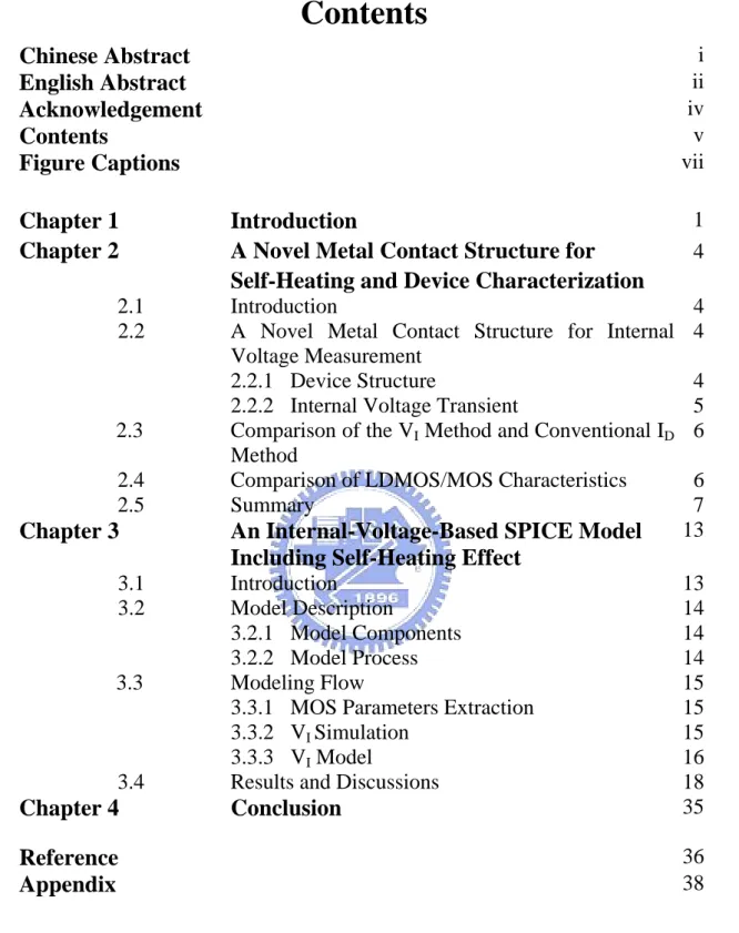
(11) self-heating effect. This thesis is organized as follows: Chapter 1 is introduction. Chapter2 demonstrates a new LDMOS characterization method by using a novel metal contact structure. Chapter3 presents a SPICE model including self-heating effect. A brief conclusion is given in Chapetr4. The organization of thesis is illustrated in Fig. 1.1.. 2.
(12) CH.2. CH.3 w/o SHE Model Internal Voltage. Self-Heating Meas.. w. SHE Model. ID VI Metal Contact Structure. Fig. 1.1 Organization of thesis. Chapter2 discusses self-heating characterization while chapter3 focuses on SPICE model including self-heating effect.. 3.
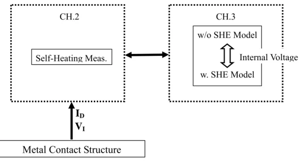
(13) Chapter 2 A Novel Metal Contact Structure for Self-Heating and Device Characterization 2.1 Introduction Self-heating effect has been recognized as one of the major reliability issues in LDMOS. [9],. particularly. when. the. device. is. utilized. in. today’s. high-voltage/high-current operations. This effect results in an increase of device temperature and a reduction of drain-current [10]. To characterize SHE, a conventional drain-current method [11] is generally used to monitor self-heating effect and the corresponding thermal time constant. In this method, a short voltage pulse is applied to gate, and drain-current is extracted from a voltage drop of an external resistor [11]. The varying drain-current in self-heating condition, however, results in a varying voltage drop across the resistor and thus an ambiguous thermal time constant. This may lead to an unreliable SHE study or SPICE model. Therefore, a new characterization method, which avoids the issue of varying voltage drop, is essential for a more accurate self-heating study.. 2.2 A Novel LDMOS Structure for Internal Voltage Measurement 2.2.1 Device Structure A cross section of the LDMOS is shown in Fig. 2.1(a). It consists of two regions, the MOS region and drift region. The voltage at the junction of two regions is indicated as the internal voltage. This internal voltage is equal to the drain voltage of 4.
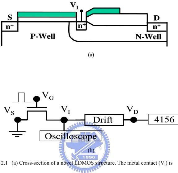
(14) the intrinsic MOS. Probing the internal voltage enables us to directly extract properties of the intrinsic MOS. To this purpose, an n+ implant is formed near the bird’s beak. The contact area is very small and thus does not affect the overall device electrical characteristics. The device used in this work was processed in a 0.18μm CMOS technology with width=20μm and channel length=3μm. The gate oxide thickness and field-oxide thickness are 110nm and 450nm respectively. The operational voltages are VG/VD =40V/40V.. 2.2.2 Internal Voltage Transient A fast transient measurement setup including a digital oscilloscope is built, as shown in Fig. 2.1(b). A gate voltage pulse and constant drain voltage (VD=40V) are applied in the VI transient measurement. The transient measurement result is shown in Fig. 2.2. At VG=40V, VI is independent of pulse time in the beginning and then decreases with pulse time. The decrease of VI is attributed to self-heating induced mobility degradation in the drift region [12][13], thus resulting in a larger drift region resistance and a smaller VI. As the applied voltage pulse is long enough, the VI becomes stable and is independent of pulse time again. Since heat in the LDMOS can be dissipated through the silicon substrate toward the backside of the wafer, heat generation/dissipation rates will reach equilibrium and thus a stable VI at a longer pulse time can be observed. In addition, at smaller gate pulse there is less power consumption and thus a smaller VI decrease.. 5.
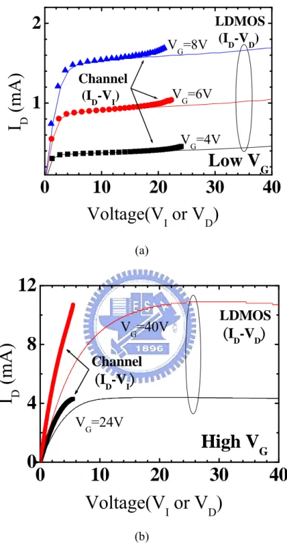
(15) 2.3 Comparison of the VI Method and Conventional ID Method For a comparison, the VI method and the conventional ID method [11] are both presented in Fig. 2.3(a) and (b) respectively. The VI in transient measurement (equal to VI w/o SHE) is extracted at gate pulse=5μs and the VI in DC measurement (equal to VI w/ SHE) is measured by Agilent 4156. At VG/VD=40V/40V, self-heating induces an 8% change in ID and a 23% change in VI, as indicated by an arrow in Fig. 2.3. A larger reduction in the VI method than in the ID method is noticed. The possible reason for a larger VI reduction can be explained by plotting the relation between ID and VI, as shown in Fig. 2.4. When self-heating occurs, the device is operating in high VG/VD. A VI reduction of 23% (ΔVI) at VG/VD=40V/40V and the corresponding ID reduction (ΔID) are indicated. It shows clearly that a large change in VI only corresponds to a small change in ID in the saturation region. Consequently, the VI method is more sensitive than then the conventional ID method for self-heating characterization.. 2.4 Comparison of LDMOS/MOS Characteristics One of the purposes of measuring VI, as we have mentioned in section 2.2.1, is to obtain characteristics of the intrinsic MOS. Therefore, a comparison of the I-V of the LDMOS (ID-VD) and the intrinsic MOS (ID-VI) in the low-VG region is shown in Fig. 2.5(a). We observe that the I-V of the intrinsic MOS and the LDMOS in linear region and saturation regions are almost identical. This implies that VI is close to VD and the LDMOS performance is dominated by the intrinsic MOS at low VG. A similar comparison of the characteristics of the intrinsic MOS and the LDMOS in the high-VG region is presented in Fig. 2.5(b). At small VD, the drain current of the intrinsic MOS and the LDMOS are very close, indicting that the intrinsic MOS still 6.
(16) dominates the LDMOS characteristics in the linear region. However, a significant current difference is observed in the saturation region, implying a large voltage drop in the drift region. Thus, the saturation characteristics of the device are controlled by both the intrinsic MOS and the drift region. This is commonly known as the quasi-saturation effect [7]. The characterization leads to a possible LDMOS modeling technique: We may use an intrinsic MOS model to control the low-VG LDMOS characteristics and another component to model the device I-V in the high VG region.. 2.5 Summary In summary, a novel internal-voltage method has been developed to characterize self-heating effect in an n-LDMOS. A self-heating induced VI transient is characterized for high gate voltage pulse. This method shows higher sensitivity than the conventional drain current method. Finally, a possible two-component LDMOS model has emerged from our comparison of LDMOS/MOS characteristics.. 7.
(17) VI S n+. D n+ N-Well. n+ P-Well (a). VG VS. VI. Drift. VD. 4156. Oscilloscope (b) Fig. 2.1 (a) Cross-section of a novel LDMOS structure. The metal contact (VI) is arranged in the bird’s beak region with an n+ implant. (b) Transient measurement setup for internal-voltage characterization.. 8.
(18) VD=40V. Voltage (V). 40. VG. 30 20 10. VI 0. 40 80 Pulse Time (μsec). Fig. 2.2 Transient VI measured at high gate voltage pulse. Self-heating induced VI decrease is observed.. 9.
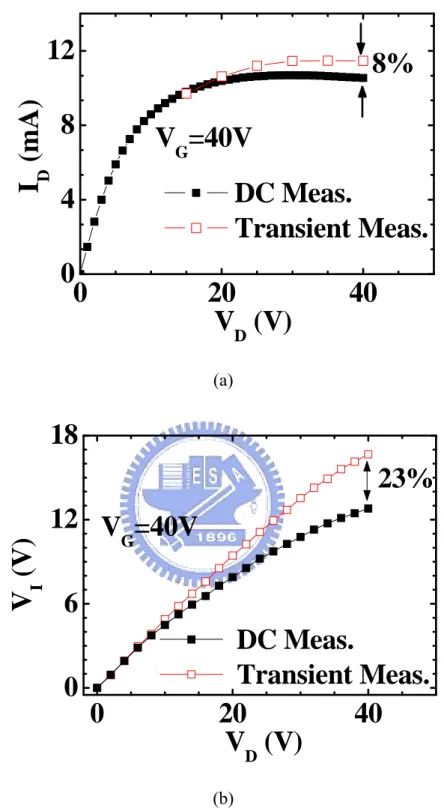
(19) ID (mA). 12. 8%. 8. VG=40V DC Meas. Transient Meas.. 4 0 0. 20 VD (V). 40. (a). 18. VI (V). 23% 12 V =40V G 6 DC Meas. Transient Meas. 20 40 VD (V). 0 0. (b) Fig. 2.3 (a) ID versus VD in SHE (DC Meas.) and SHE-free (Transient Meas.) conditions. At VG/VD=40V/40V, SHE induces 8% change in drain current. (b) VI versus VD in SHE and SHE-free conditions. A 23% change caused by SHE is seen at VG/VD=40V/40V. 10.
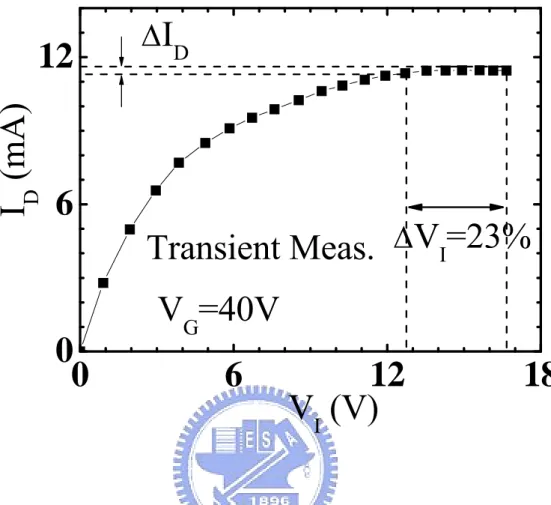
(20) ID (mA). 12. 6. 0 0. ΔID. Transient Meas. ΔVI=23% VG=40V 6. 12 VI (V). Fig. 2.4 ID versus VI at VG=40V. In the saturation region, a VI change of 23% corresponds to a relatively small change in ID.. 11. 18.
(21) ID (mA). 2. 1. LDMOS VG=8V (ID-VD) Channel (ID-VI). VG=6V VG=4V. 0. Low VG 10 20 30 40 Voltage(VI or VD) (a). ID (mA). 12 8. VG=40V. LDMOS (ID-VD). Channel (ID-VI). 4 VG=24V. 0 0. High VG 10 20 30 Voltage(VI or VD). 40. (b) Fig. 2.5 (a) Current versus voltage of the LDMOS (ID-VD) and the intrinsic MOS (ID-VI) in the low-VG region. The I-V of the intrinsic MOS and the LDMOS in linear region and saturation regions are almost identical. (b) High-VG current versus voltage of the LDMOS and the intrinsic MOS. A significant current difference is observed in the saturation region. 12.
(22) Chapter 3 An Internal-Voltage-Based SPICE Model Including Self-Heating Effect 3.1 Introduction The efficiency of the LDMOS circuit depends tremendously on the device model. A precise model greatly enhances the device performance. However, characterization of LDMOS is rather difficult compared to conventional MOSFET due to the diverse nature of the channel region and drift region. A major obstacle is the characterization of drift region because of its complex dependence on external terminal voltages. A common approach to cope with this issue is by using the internal voltage to separate the channel and drift region and model the two regions independently. Many modeling approaches have been developed to solve the internal voltage [3-8]. Most of them used a numerical iteration procedure to solve the internal voltage with numerous fitting parameters [3-6]. Others solve for the internal voltage explicitly by equating the channel current with the drift region current [7-8]. However, none of the studies take into account the correlation between the internal voltage and self-heating effect. In this chapter, a VI-based LDMOS model including self-heating effect is presented. We have also developed a VI simulation method, which produces the corresponding internal voltage of each drain current. Hence, our VI-based model can be applied without actual fabrication of a special structure for VI measurement. A simplified VI equation with four fitting parameters is given explicitly in terms of the external terminal voltages. The model is finally simulated by an HSPICE simulator.. 13.
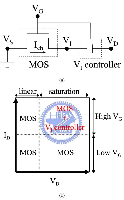
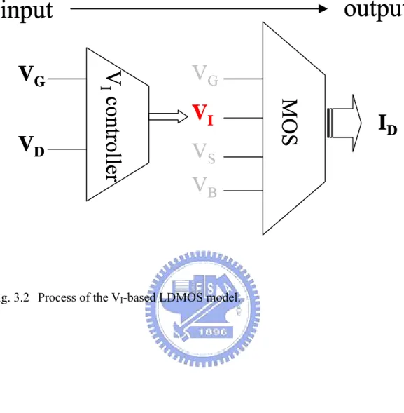
(23) 3.2 Model Description 3.2.1 Model Components An equivalent circuit of the LDMOS is shown in Fig. 3.1(a). The circuit model consists of two components, an intrinsic MOS and a VI controller. We denote the current flow through the MOS model as Ich to distinguish it from the drain current ID. Fig. 3.1(b) illustrates the operation regions controlled by the two components respectively. The low-VG region and the linear high-VG region are controlled by the MOS model. The saturation high-VG region is controlled by the MOS model and the VI controller.. 3.2.2 Model Process Fig. 3.2 is an illustration of our SPICE model process. First, the external gate and drain voltages are the input to the VI controller. The VI controller generates the corresponding VI, which is then set as the input drain voltage of the MOS model. After that, the MOS model produces the final ID according to its input voltages. The operation of the MOS model is well understood. Hence, we will explain how the VI controller generates the correct VI. The process of the VI controller is specified in Fig. 3.3. When a pulse gate or drain voltage is applied and self-heating is induced, VI controller generates two terms. One is the VI at pulse time t=0, which equals the non-self-heating VI. The other term is the self-heating induced VI change at pulse time t>0. In this way, a model value of VI at any pulse time t is obtained. After introducing our model concept, we will demonstrate in detail how the model is built in the next section.. 14.
(24) 3.3 Modeling Flow A specially-designed LDMOS modeling flow is shown in Fig. 3.4, including five steps: (1) and (2) MOS parameters extraction, (3) VI simulation, (4) VI model, and (5) LDMOS model.. 3.3.1 MOS Parameter Extraction In step 1, the measurement I-V data of LDMOS is divided into the low-VG data and the high-VG data. The low-VG MOS model is built on the MOS parameters extracted from the LDMOS low-VG data. A comparison of the measurement data and the fitting results after step 1 is shown in Fig. 3.5. Then, the MOS model is extended to high-VG using the high-VG data in the linear region in step 2. Fitting results after step 2 is shown in Fig. 3.6. Step 1 and 2 are actually carried out at the same time, using built-in MOSFET model in BSIM3v3. At this point, we have completed the MOS model, which will be utilized in the next step—VI simulation.. 3.3.2 VI Simulation In this step we will deal with the LDMOS I-V in the high VG/VD region, which is supposed to be controlled by both the MOS model and the VI controller. Our goal is to obtain the corresponding VI of each ID, so that in the next step we can build the VI model based on the simulation VI data. The VI simulation method is illustrated in detail in Fig. 3.7. Using the LDMOS drain current as an input current source to the MOS model, we can obtain the corresponding output VI. A typical VI simulation result is illustrated in the inset of Fig. 3.7. Note that the VI-VD simulation result has the same saturation characteristics of the LDMOS ID-VD measurement. Consequently, VI is limited in the saturation region and the current produced by the MOS model will also. 15.
(25) exhibit the same saturation characteristics as the LDMOS measurement current.. 3.3.3 VI Model The VI model describing the internal voltage transient is established by integrating a non-self-heating VI model with a self-heating induced VI change. The non-self-heating VI model is denoted by VI (t=0), implying the VI at pulse time t=0. VI equations with both VG and VD dependence are used in the non-self-heating model, which are derived as follows. First, an LDMOS current equation with two fitting parameters, θmd and n, is expressed as:. I D (VG , VD ) ≈. μ0 W V ⋅ Cox ⋅ ⋅ (VG − Vt − D ) ⋅ VD n L 1 + θ md ⋅ (VG − Vt ) 2. The MOS model current in the linear region is expressed as:. I ch (VG , VI ) ≈. V W ⋅ Cox ⋅ μ0 ⋅ (VG − Vt − I ) ⋅ VI 2 L. Since the LDMOS current is equal to the intrinsic MOS current, equating the currents we get an expression for VI:. VD ) ⋅ VD 2 VI (VG , VD ) ≈ (VG − Vt ) − (VG − Vt ) 2 − 2 ⋅ 1 + θ md ⋅ (VG − Vt ) n (VG − Vt −. We arrive at an expression for the LDMOS current:. 16. (1).
(26) I D (VG , VI ) =. W V ⋅ Cox ⋅ μ0 ⋅ (VG − Vt − I ) ⋅VI 2 L V W ⋅ Cox ⋅ μ0 ⋅ (VG − Vt − Isat ) ⋅VIsat 2 L. VD ≤ VDsat VD > VDsat. The linear drain current is simply obtained using equation 1 for VI. For the current in the saturation region, VI is substituted by VIsat,. VDsat ) ⋅ VDsat 2 where VIsat (VG ) = VI |VD =VDsat = (VG − Vt ) − (VG − Vt ) 2 − 2 ⋅ 1 + θ md ⋅ (VG − Vt ) n (VG − Vt −. and. VDsat (VG ) =. (2). (VG − Vt ) , with fitting parameter γ. 1 + γ ⋅ (VG − Vt ). So far we have acquired an expression for linear region VI (equation 1) and an expression for saturation region VI (equation 2). We now introduce an effective VI [14] to express VI in both linear and saturation regions as a single equation:. 1 VI ,eff (VG , VD ) = VIsat − ⋅ [VIsat − VD − Δ + (VIsat − VD − Δ ) 2 + 4Δ ⋅ VIsat ] 2. (3). There is a fitting parameter Δ determining the degree of smoothness in the quasi-saturation transition. Equation 3 includes four fitting parameters: θmd, n, γ and Δ. Equations 1, 2 and 3 are plotted in Fig. 3.8 to further explain the concept. Fig. 3.9 shows the resulting non-self-heating VI model built by the model equations. The LDMOS transient characteristics when a gate or drain voltage pulse is applied are controlled by the ΔVI transient model. Fig. 3.10 shows the transient ID and the corresponding transient VI obtained by VI simulation method. In an attempt to 17.
(27) describe the transient VI by an exponential decay function, our model utilizes an RC sub-circuit shown in Fig. 3.11. The sub-circuit is composed of three components: a current source, R and C. RC is the time constant of the VI transient. The voltage drop across RC is modeled as the SH-induced VI change, denoted as ΔVI(t). In transient operation, the current source starts to charge the capacitor C and ΔVI(t) increases. When the capacitor becomes fully-charged, ΔVI(t) maintains a constant value, which is equal to the value β extracted from Fig. 3.10. Also extracted from Fig. 3.10 is the time constant τC. A comparison between the simulation and model ΔVI(t) and VI(t) is shown in Fig. 3.12. The VI(t) is modeled as VI(t) = VI(t=0)-ΔVI(t). Time-dependent VI and ΔVI equations can be expressed as. VI (t ) = VI (∞) + β ⋅ exp(− ΔVI (t ) = β ⋅ [1 − exp(−. t. τC. t. τC. ). )]. By incorporating the MOS model and the VI model, the macro model is finally acquired. The model is performed by an HSPICE simulator and the modeling results will be presented in the next section.. 3.4 Results and Discussions In the following figures, symbols correspond to the measurement data, while the solid lines represent the LDMOS model. Fig. 3.13 shows the drain current transient when a gate voltage pulse is applied. Since our VI model has described the VI simulation transient correctly, the macro model can also successfully describe the ID measurement transient. 18.
(28) The model ID transient at t=0 and t=30μs are extracted as the model drain current w/o SHE and w/ SHE respectively at various VG/VD to form the ID versus VD results in Fig. 3.14. In the low-VG region, no self-heating is observed and only one curve is shown for each gate voltage. By a comparison with the MOS model in step 1, we notice that the macro model current level is slightly lower than the MOS model current level in the low VG region, which is due to subsequent use of the VI controller. In the high VG region, both SHE-free and SHE drain currents are shown for VG=24V and VG=40V. Once again, at VG=40V the model current is largely suppressed compared to the MOS model current and matched with the LDMOS measurement current level. This again is due to the VI controller which limits the VI value and restricts the MOS model output current. In Fig. 3.15(a), modeling results of the linear characteristics of the LDMOS device are presented. An accurate linear drain current and transconductance Gm are achieved and thus the VTH of the model is matched with that of the device. Note that as VD is small, model equation 2 becomes VI≈VD, implying that the device characteristic is dominated by the MOS model. Fig. 3.15(b) depicts the saturation characteristics of the LDMOS device. The drain current in the SHE condition exhibits serious quasi-saturation effect, indicating the effect of drift region on the saturation characteristics of the high-VG region. The drain currents in both high-VG and low-VG regions are well described by our model. A good agreement between model and measurement results has proven that the VI controlled self-heating model is successfully used in the LDMOS device.. 19.
(29) VG VS. VI. Ich MOS. VD VI controller. (a). linear. saturation. MOS. MOS + VI controller. High VG. MOS. MOS. Low VG. ID. VD (b) Fig. 3.1 (a) Equivalent circuit model of the LDMOS device. The MOS represents the channel region while the VI controller accounts for the drift region. (b) Illustration of different operation regions controlled by each component.. 20.
(30) output. input VG VI VS VB. Fig. 3.2 Process of the VI-based LDMOS model.. 21. MOS. VD. VI controller. VG. ID.
(31) VI controller VG. VI w/o SH +. t=0. Self-heating Pulse time. VD. t>0. VI (t). ΔVI transient. Fig. 3.3 Process of the VI controller. Here self-heating effect is taken into account.. 22.
(32) Low VG Raw data. 1. MOS (Low VG) Model 2. LDMOS ID-VD High VG Raw data. -. MOS (High VG) Model. VI simulation data. 3. 4. ΔVI transient Self-Heating Model. LDMOS Model. 5. MOS Model. +. +. VI (t=0). VI Model. VI Model (including self-heating). Fig. 3.4 A specially-designed modeling flow to set up the MOS model and the VI model. Five steps are indicated, including (1) and (2) MOS parameter extraction, (3) VI simulation, (4) VI model, and (5) LDMOS macro model.. 23.
(33) ID , Ich (mA). 3. Symbol: Meas. ( ID-VD ) Line: MOS Model (Ich-VI). VG=10V. 2 1. 4V. 0 0. 20 VD , VI (V). 40. (a). ID , Ich (mA). 20. Symbol: Meas. ( ID-VD ) Line: MOS Model (Ich-VI). 10. VG=40V VG=16V. 0 0. 20 VD , VI (V). 40. (b) Fig. 3.5 A comparison of measurement data and model fitting results after step 1. (a) Low-VG and (b) High-VG.. 24.
(34) ID , Ich (μA). 180 Low VG. High VG VD=VI=0.1V. 90. Symbol: Meas. ( ID). 0. Line: MOS Model ( Ich). 0. 20 VG (V). 40. Fig. 3.6 A comparison of measurement data and model fitting results after step 2.. 25.
(35) High VG Raw data. G. VG. 3. 15. VI simulation. VS. 10. VI. VG=40V. 5. w/o SH w. SH. Ich LDMOS (Meas.). VI simulation data. MOS Model. 0. 20 VD (V). VI (V). ID. (High V ) - MOSModel. 0 40. Fig. 3.7 A special simulation method to obtain internal voltage data from the input drain current. The MOS parameters are extracted from step 1 and 2. Typical VI simulation result is plotted under self-heating (w. SH) and non-self-heating (w/o SH) conditions.. 26.
(36) 12. VI (V). VG=20V 6 by Eq.1 by Eq.2 by Eq.3. 0 0. 20 VD (V). 40. Fig. 3.8 Model VI equations plotted at VG=20V. Eq.1 represents VI in the linear region while Eq.2 depicts saturation VI. Eq.3 is the effective VI for both linear and saturation regions.. 27.
(37) 15 VD=40V. w/o SH. VI (V). 10 5. Symbol: VI Simulation Line: VI Model. 0 0. 20 VG (V). 40. (a). VI (V). 15 V =40V G. w/o SH. 10 5. Symbol: VI Simulation Line: VI Model. 0 0. 20 VD (V). 40. (b) Fig. 3.9 Comparison of the non-self-heating VI simulation data and the VI model built by model equations. (a) VI-VG and (b) VI-VD.. 28.
(38) ID (mA). 12. VG=VD=40V. 10 Meas. ID. VI (V). VI Simulation Method. 12 Simulation VI. β. 9 τC -30 -20 -10 0 10 20 30 Pulse Time (μsec). Fig. 3.10 ID transient and the corresponding simulation VI transient. The SH-induced total VI change β and the time constant τC are extracted from the transient VI.. 29.
(39) ΔVI(t). C. Fig. 3.11 RC sub-circuit for modeling of transient VI change.. 30. R.
(40) VI and ΔVI (V). 12. VG=VD=40V. VI(t). 9. VI(t)=VI(0)-ΔVI(t). 6. Simulation Model. ΔVI(t). 3 0. 10 20 Pulse Time (μsec). Fig. 3.12 Simulation and model ΔVI(t) and VI(t).. 31. 30.
(41) ID (mA). 12 8. Meas. LDMOS Model. 4 0. VG=VD=40V 0. 10 20 Pulse Time (μsec). Fig. 3.13 Modeling result of the drain current transient at VG=VD=40V.. 32. 30.
(42) ID (mA). 3. Symbol: Meas. (LDMOS) Line : LDMOS Model. VG=10V. 2 1 4V 0 0. 40. 20 VD (V) (a). 40V. ID (mA). 12. SHE. 8 VG=24V. 4. Symbol: Meas. (LDMOS) Line: LDMOS Model. 0 0. 20. VD (V). 40. (b) Fig. 3.14 Comparison of measurement and model ID versus VD at (a) Low-VG and (b) High-VG. The model drain current values w/o SHE and w/ SHE are extracted from the model ID transient at t=0 and t=30μs respectively.. 33.
(43) 2. Symbol : Meas. (LDMOS) Line : LDMOS Model. 1 VD=0.1V. 0 0. 0 40. 20 VG (V) (a). ID (mA). 12. w/o SH. VD=40V. w. SH 6. 0 0. Symbol: Meas. (LDMOS) Line: LDMOS Model. 20 VG (V). 40. (b) Fig. 3.15 Modeling results of ID versus VG in (a) linear region and (b) saturation region.. 34. -5. 90. Gm (10 A/V). ID (mA). 180.
(44) Chapter 4 Conclusion A special LDMOS structure with an extra metal contact for internal voltage measurement has been fabricated and self-heating effect characterization by the internal voltage method is demonstrated. Self-heating induces more change in VI than in ID because of the nature of the device in the saturation region. A comparison of the intrinsic MOS and the LDMOS characteristics is presented. The intrinsic MOS dominates the low-VG region of the device properties, whereas drift region dominates the high VG/VD region. A complete VI-based LDMOS model including self-heating effect is presented. Self-heating induced transient VI change is accurately described by an RC sub-circuit. We also put forth simplified explicit VI equations with only four major fitting parameters (Δ, γ, θmd, n). Successful use of the LDMOS model in HSPICE simulator has proven that our LDMOS model can reach a very good agreement between measurement and model.. 35.
(45) 簡. 歷. 姓名: 熊勖廷 性別: 男 生日: 民國 73 年 6 月 9 日 籍貫: 湖北省黃陂縣 地址: 台南縣新營市健康路 213 巷 17 號 學歷: 國立清華大學電機工程學系. 91.9-95.6. 國立交通大學電子工程研究所碩士班 95.9-97.6 碩士論文題目:. 利用特殊接觸電極進行橫向擴散元件之 特性分析與 SPICE 模型建立 Characterization and SPICE Modeling of Lateral Diffused MOS by using a Novel Metal Contact Structure. 47.
(46) Reference. [1]. B. J. Baliga, “An overview of smart power technology”, IEEE Elect. Dev., vol. 38, pp. 1568, July 1991. [2]. Murari B., “Smart power ICs”, New York:Springer; 1995. [3]. Yeonbae Chung and D. E. Burk, “A physically based DMOS transistor model implemented in SPICE for advanced power IC TCAD”, IEEE International Sym. on Power Semiconductor Devices and ICs (ISPSD), pp.340-345, 1995. [4]. Merit Y. Hong and Dimitri A. Antoniadis, “Theoretical analysis and modeling of submicron channel length DMOS transistors”, IEEE Trans. On Electron Devices, vol. 42, pp.1614-1622, 1995. [5]. Y. Chung, “LADISPICE-1.2: a nonplanar-drift lateral DMOS transistor model and its application to power IC TCAD”, IEE Proc. Circuits Devices and Systems, vol.147, pp.219-227, 2000. [6]. Yeong-Seuk Kim, Jerry G. Fossum, and Richard K. Williams, “New physical insights and models for high-voltage LDMOST IC CAD”, IEEE Trans. On Electron Devices, vol. 38, pp.1641-1649, 1991. [7]. Annemarie C. T. Aarts and Willy J. Kloosterman, “Compact Modeling of High-Voltage LDMOS Devices Including Quasi-Saturation”, IEEE Trans. on Electron Devices, vol. 53, pp.897-902, 2006. [8]. Annemarie Aarts, Nele D’Halleweyn, and Ronald van Langevelde, “A. 36.
(47) Surface-Potential-Based High-Voltage Compact LDMOS Transistor Model”, IEEE Trans. on Electron Devices, vol. 52, pp.999-1007, 2005 [9]. C.C. Cheng, J.F. Lin, Tahui Wang, T.H. Hsieh, J.T. Tzeng, Y.C. Jong, R.S. Liou, Samuel C. Pan, and S.L. Hsu, “Impact of Self-Heating Effect on Hot Carrier Degradation in High-Voltage LDMOS”, IEEE International Electron Device Meeting (IEDM), pp.881-884, 2007. [10]. Y. K. Leung, S. C. Kuehne, Vincent S. K. Huang, Cuong T. Nguyen, Amit K. Paul, James D. Plummer, and S. Simon Wong, “Spatial Temperature Profiles Due to Nonuniform Self-Heating in LDMOS’s in Thin SOI”, IEEE Trans. Electron Devices Lett. vol. 18, pp.13-15, 1997. [11]. C. Anghel, R. Gillon, and A. M. Ionescu, “Self-Heating Characterization and Extraction Method for Thermal Resistance and Capacitance in High Voltage MOSFETs”, IEEE Trans. Electron Devices Lett. Vol. 25, pp.141-143, 2004. [12]. Emil Arnold, Howard Pein, and Sam P. Herko, “Comparison of Self-heating Effects in Bulk-silicon and SOI high-voltage Devices”, IEDM Tech. Dig., pp.813-816, 1994. [13]. Gary M. Dolny, Gerald E. Nostrand, and Kevin E. Hill, “The effect of temperature on lateral DMOS transistors in a power IC technology”, IEEE Trans. on Elect. Dev., vol. 39, pp.990-995, 1992. [14]. William Liu, MOSFET Models for SPICE Simulation Including BSIM3v3 and BSIM4, New York, Wiley, p.30, 2001. 37.
(48) Appendix MOS Model Parameters extracted by BSIM3v3. .model. nch_asy. nmos. (. +level = 49 +lmin. = 1.7e-006. +tref. +lmax. = 1.7e-006. +xl. +wmin. = 2e-005. +xw. +wmax. = 2e-005. +lmlt. = 25 =0 =0 =1. +version = 3.24. +wmlt. =1. +mobmod. +ld. =0 =0. =1. +capmod. =3. +llc. +nqsmod. =0. +lwc. =0. +binunit = 1. +lwlc. =0. +stimod. +wlc. =0. =0. +paramchk= 0. +wwc. =0. +binflag = 0. +wwlc. =0. +vfbflag = 0. +tox. = 1.117e-007. +hspver. = 2000.2. +wint. =0. +lref. = 1e+020. +lint. =0. +hdif. = 5.175e-006. +wref. = 1e+020. 38.
(49) +ldif. =0. +dvt2. = -0.032. +ll. =0. +dvt0w. =0. +dvt1w. = 5300000. +dvt2w. = -0.032 = 1.67e+016. +wl +lln. =0 =1. +wln. =1. +nch. +lw. =0. +voff. +ww +lwn +wwn +lwl. =0. = 0.165. +nfactor = 1. =1 =1 =0. +cdsc. = 0.00024. +cdscb. =0. +cdscd. =0 =0. +wwl. =0. +cit. +cgbo. = 1e-013. +u0. = 0.08346. +xpart. =1. +ua. = 1.025e-008. +vth0. = 0.7347. +ub. = -2.32e-018. +k1. = 0.53. +uc. = -4.65e-011. +k2. = -0.0186. +ngate. =0. +k3. = 80. +xj. = 1.7e-006. +k3b. =0. +w0. = 2.5e-006. +nlx. = 1.74e-007. +prwg. =0. +dvt0. = 2.2. +prwb. =0. +dvt1. = 0.53. +wr. =1. 39.
(50) +rdsw. =0. +delta. = 0.016. +a0. = 0.0099. +eta0. = 0.05395. +ags. = -2e-012. +etab. = -0.07. +a1. =0. +dsub. = 0.56. +a2. =1. +elm. =5. +b0. =0. +alpha1. =0. +b1. =0. +clc. = 1e-007 = 0.6. +vsat. = 105200. +cle. +keta. = -0.047. +ckappa = 0.6. +dwg. =0. +cgdl. =0. +dwb. =0. +cgsl. =0. +alpha0 = -2e-012. +vfbcv. = -1. +beta0. +acde. =1. +moin. = 15. +pclm. = 30 = 4.7e-012. +pdiblc1 = 0.0871. +noff. =1. +pdiblc2 = 0.0005507. +voffcv. =0. +pdiblcb = -2e-012. +kt1. = -0.11. +drout. = 0.56. +kt1l. =0. +pvag. =0. +kt2. = 0.022. +pscbe1 = 4.198e+008. +ute. = -1.5. +pscbe2 = 5e-006. +ua1. = 4.31e-009. 40.
(51) +ub1. = -7.61e-018. +rd. =0. +uc1. = -5.6e-011. +rdc. =0. +prt. =0. +rs. =0. +at. = 33000. +rsc. =0. +xti. =0. +noimod. =1. +noia. = 1e+020. +acm. +noib. = 50000. +calcacm = 0. +noic. = -1.4e-012. +nj. +em. = 41000000. +pbsw. = 12. =1 = 0.8. +af. =1. +ptc. =0. +ef. =1. +tt. =0. +kf. =0. +ijth. = 0.1. +gdsnoi. =1. +tcj. =0. +rsh. =0. +tcjsw. =0. +js. = 0.0001. +tcjswg. =0. +jsw. =0. +tpb. =0. +cj. = 0.0005. +tpbsw. =0 =0. +mj. = 0.5. +tpbswg. +cjsw. = 5e-010. ). +mjsw. = 0.33. +pb. =1. 41.
(52)
數據
+7

相關文件
Finally, we use the jump parameters calibrated to the iTraxx market quotes on April 2, 2008 to compare the results of model spreads generated by the analytical method with
We showed that the BCDM is a unifying model in that conceptual instances could be mapped into instances of five existing bitemporal representational data models: a first normal
The Hull-White Model: Calibration with Irregular Trinomial Trees (concluded).. • Recall that the algorithm figured out θ(t i ) that matches the spot rate r(0, t i+2 ) in order
The Hull-White Model: Calibration with Irregular Trinomial Trees (concluded).. • Recall that the algorithm figured out θ(t i ) that matches the spot rate r(0, t i+2 ) in order
Moreover, through the scholar of management, Michael Porter's Five Forces Analysis Model and Diamond Model make the analysis of transport industry at port, and make the
The first row shows the eyespot with white inner ring, black middle ring, and yellow outer ring in Bicyclus anynana.. The second row provides the eyespot with black inner ring
[4] Hiroyuki, O., “Sound of Linear Guideway Type Recirculating Linear Ball Bearings” , Transactions of the ASME, Journal of Tribology, Vol. Part I: design and Construction” ,
The temperature angular power spectrum of the primary CMB from Planck, showing a precise measurement of seven acoustic peaks, that are well fit by a simple six-parameter
