國 立 交 通 大 學
電子工程學系 電子研究所
碩士論文
十億級資料傳輸室內無線 SC/OFDM 接收機之
等化器
Design of Equalizer for Multi-Gbps Transmission
Indoor Wireless SC/OFDM Receiver
研 究 生:葉福鈞
指導教授:周世傑 教授
十億級資料傳輸室內無線 SC/OFDM 接收機之等化器
Design of Equalizer for Multi-Gbps Transmission Indoor
Wireless SC/OFDM Receiver
研 究 生:葉福鈞
Student:Fu-Chun Yeh
指導教授:周世傑 教授
Advisor:Prof. Shyh-Jye Jou
國 立 交 通 大 學
電子工程學系 電子研究所碩士班
碩士論文
A Thesis
Submitted to Department of Electronics Engineering & Institute of Electronics College of Electrical and Computer Engineering
National Chiao Tung University in partial Fulfillment of the Requirements
for the Degree of Master of Science in
Department of Electronics Engineering July 2011
Hsinchu, Taiwan, Republic of China
十億級資料傳輸室內無線 SC/OFDM 接收機之等化器
研究生:葉福鈞 指噵教授:周世傑 教授 國立交通大學 電子工程學系 電子研究所碩士班摘要
本論文針對IEEE 802.15.3c標準中的雙模式(單載波和正交分頻多工)提出適 應性最小均平方(LMS)頻域等化器搭配最小平方(LS)頻域通道估測(LS-LMS FDE), 和多重路徑干擾消除(MPIC)時域等化器搭配格雷(Golay)序列時域通道估測 (Golay-MPIC TDE)。此兩種方法皆可以共用雙模式中的硬體,以達到降低硬體複 雜度的目的。LS-LMS FDE使用了最小均平方的適應演算法以及最小平方的通道估 測來加速收斂速度同時也能保持低運算複雜度。模擬的結果顯示在訊雜比為12dB 時,未具有任何編碼保護下的位元錯誤率,在單載波和正交分頻多工模式中,分 別可達到6.01*10-4 和9.68*10-3 。整體的等效邏輯閘數除了快速傅立葉轉換模組外, 為41.5萬個邏輯閘,其中有69%是雙模式共用的硬體。當操作頻率在400MHz時, 不包含快速傅立葉轉換模組的功率消耗只有81.27毫瓦。而Golay-MPIC TDE使用 多重路徑干擾消除演算法降低硬體複雜度及格雷序列通道估測來消除雜訊干擾。 當訊雜比為12dB時,未具有任何編碼保護下的位元錯誤率,在單載波和正交分頻 多工模式中,分別可達到2.53*10-4 和4.22*10-5 。整體的等效邏輯閘數為40.5萬個 邏輯閘,其中有99%是雙模式共用的硬體。操作頻率在400MHz時,功率消耗只有 88毫瓦。 本論文提出的頻域和時域等化器,分別整合進兩個室內無線傳輸基頻接收機 中。基於高速和面積使用率的考量,硬體合成使用了 65 奈米 1 伏特 1P9M CMOS 製程。LS-LMS FDE 晶片的核心部分占了 7.81mm2 ,使用率是 65.91%。操作頻率為和 5.28Gbps,功率消耗 793.98 毫瓦。符號邊界同步估測器與此 LS-LMS FDE 共 用的記憶體佔了 32.68%。而 Golay-MPIC TDE 晶片的核心部分占了 7.95 mm2 ,使 用率是 88.93%。操作頻率為 336.7 MHz,資料傳輸率在單載波和正交分頻多工模 式中,分別可達到 3.52Gbps 和 5.28Gbps,功率消耗為 1.12 瓦。符號邊界同步 估測器、相位雜訊消除器與此Golay-MPIC TDE 共用的記憶體佔了 37%。
Design of Equalizer for Multi-Gbps Transmission
Indoor Wireless SC/OFDM Receiver
Student:Fu-Chun Yeh Advisor:Prof. Shyh-Jye Jou Department of Electronics Engineering
Institute of Electronics National Chiao Tung University
Abstract
This thesis proposes an adaptive LS-LMS FDE and LOS Goaly-MPIC TDE that can satisfy the dual mode (SC and HSI) specifications of IEEE 802.15.3c. The hardware of both methods can be shared by SC and HSI mode to reduce hardware complexity. The LS-LMS FDE combines LMS adaptive algorithm with LS channel estimation. The LMS algorithm has the advantage of low computational complexity and sufficient convergence speed with the aid of LS channel estimation. The simulation results show that the LS-LMS FDE can achieve 6.01*10-4 BER in SC mode and 9.68*10-3 BER in HSI mode (both uncoded) at SNR 12 dB. The total area is about 415K gate-count with 69% shared among SC and HSI mode except 2 FFT. The power consumption excluding FFT is only 81.27 mW when working at 400MHz. On the other hand, the Golay-MPIC TDE uses Multi-path Interference Cancellation (MPIC) equalization with Golay sequence-aided channel estimation. The MPIC algorithm can reduce the hardware complexity unlike traditional time-domain equalizer and Golay sequence-aided channel estimation will eliminate the AWGN noise. The Golay-MPIC TDE can achieve 2.53*10-4 BER in SC mode and 4.22*10-5 BER in HSI mode (both uncoded) at SNR 12dB. The total area is about 405K
mW when working at 400 MHz.
The proposed different domain architectures are integrated in two indoor wireless communication baseband receiver systems. For the high speed and area efficiency considerations, the overall system designs are implemented using 65 nm 1P9M CMOS GP process under supply voltage 1.0 V. The LS-LMS FDE chip occupies 7.81mm2 core area with 65.91% utilization, and the clock rate is 333 MHz. The data rate of SC and HSI mode can achieve 3.52 Gbps and 5.28 Gbps, respectively. Also, the power consumption is793.98 mW. The shared memory is 32.68% of the baseband system which is shared by BD and FDE blocks. The core area of Golay-MPIC TDE chip is 7.95 mm2 with 88.93% utilization, and the clock rate is 336.7 MHz. The data rate of SC and HSI mode can achieve 3.52 Gbps and 5.28 Gbps, respectively. Also, the power consumption is 1.12 W. The BD, TDE and PNC blocks use the same shared memory which is 37% of the baseband system.
致 謝
在碩士兩年生涯裡,最感謝的是周世傑教授,不論是學術課業上的指導,還 是生活健康上的照顧,老師都無私地給予我們幫助,因此我才能順利地完成研究。 然後要感謝口試委員,陳紹基教授、李鎮宜教授和劉志尉教授,委員們在口試時 的建議和指導,讓我的研究更加的完善。再來要感謝的是實驗室的同學們:首先 是庭楨、瑋昌、盈志、紹維、代暘、為凱、雅雪、祥譽學長姐們,還有亦瑋、以 樂、佳怡,他們給我很多研究上的建議,並且也為生活中帶來了許多樂趣。也感 謝幫忙完成快速傅立葉轉換模組的紳睿學長,讓晶片能夠順利完成。接下來要感 謝的是幫助過我的所有師長和朋友。最後要感謝支持我的家人,讓我能安心地完 成學業。 葉福鈞 於新竹交通大學 100.07Contents
Chapter 1 Introduction ... 4
1.1 Indoor Wireless Communication Standards for 60 GHz with Multi-Gbps Transmission ... 4
1.2 Motivation ... 6
1.3 Thesis Organization ... 7
Chapter 2 Overview of Multi-Gbps Transmission Indoor Wireless Communication Standards ... 8
2.1 Comparison of IEEE 802.15.3c and IEEE 802.11ad ... 8
2.2 IEEE 802.15.3c Specifications ... 10
2.2.1 Basic Specifications ... 10
2.2.2 Equalization Related Specifications ... 12
2.2.3 Channel Model ... 16
Chapter 3 SC/OFDM Dual-Mode Frequency and Time Domain Equalizer ... 20
3.1 Review of Frequency Domain Equalization (FDE) [11] ... 20
3.1.1 Channel Estimation ... 22
3.1.2 Adaptive Equalization ... 24
3.2 Review of Time Domain Equalizer (TDE) ... 27
3.2.1 Multi-path Interference Cancellation ... 29
3.2.2 Golay-Sequence Aided Channel Estimation [15] ... 31
3.3 Proposed Architecture for IEEE 802.15.3c ... 33
3.3.1 Proposed Adaptive LS-LMS FDE [11] ... 33
3.3.2 Proposed LOS Golay-MPIC TDE ... 36
Chapter 4 Architecture Design and Performance Analysis ... 41
4.1.1 Proposed Adaptive LS-LMS FDE and Baseband Receiver [11] ... 44
4.1.2 Proposed LOS Golay-MPIC TDE and Baseband Receiver ... 47
4.2 Sub-block Architecture Design ... 50
4.2.1 Optimised Golay Correlator (OGC)... 50
4.2.2 Divider Free LS Method [11] ... 52
4.2.3 FFT/IFFT Design Specifications ... 57
4.3 Synthesis and Simulation Results ... 58
4.3.1 Proposed Adaptive LS-LMS FDE ... 59
4.3.2 Proposed LOS Golay-MPIC TDE ... 61
4.4 Comparison of Adaptive LS-LMS FDE and MPIC Golay-MPIC TDE ... 63
Chapter 5 Baseband Design and Chip Implementation ... 65
5.1 Adaptive LS-LMS FDE in Baseband Receiver [34] ... 65
5.1.1 Chip Integration and Implementation Result ... 65
5.1.2 Measurement Consideration ... 69
5.2 LOS MPIC Golay-MPIC TDE in Baseband Receiver ... 73
5.2.1 Chip Integration and Implementation Result ... 73
5.2.2 Measurement Consideration ... 76
Chapter 6 Conclusion and Future Work ... 77
6.1 Architecture Design Summary ... 77
6.2 Chip Implementation Summary ... 78
6.3 Future Work ... 78
List of Tables
Table 2-1 Comparison of 802.15.3c and 802.11ad ... 9
Table 2-2 SC mode specifications ... 11
Table 2-3 HSI mode specifications ... 12
Table 2-4 Golay sequences ... 13
Table 4-1 System parameters ... 43
Table 4-2 FDE Hardware comparison between SC and HSI mode ... 46
Table 4-3 TDE Hardware comparison between SC and HSI mode ... 49
Table 4-4 Number of calculation for each corrlator ... 52
Table 4-5 Specifications of FFT/IFFT in the proposed FDE ... 58
Table 4-6 LS-LMS FDE for SC and HSI mode synthesis result ... 60
Table 4-7 Golay-MPIC TDE for SC and HSI mode synthesis result... 61
Table 4-8 Synthesis result of LS-LMS FDE and Golay-MPIC TDE ... 63
Table 4-9 Computation complexity of LS-LMS FDE and Golay-MPIC TDE ... 64
Table 4-10 Comparison of LS-LMS FDE and Golay-MPIC TDE ... 64
Table 5-1 Area and power comparison of 32×32 dual port memory and register ... 67
Table 5-2 1st chip summary (using LS-LMS FDE) ... 68
Table 5-3 Power measurement of 1st chip ... 69
Table 5-4 Comparison of old and new TSMC 65nm GP process libraries ... 74
List of Figures
Fig. 1-1 Unlicensed band at 60 GHz in different countries ... 5
Fig. 2-1 RF band plan ... 11
Fig. 2-2 CMS frame format ... 13
Fig. 2-3 SC PHY frame format ... 14
Fig. 2-4 SC PHY preamble structure ... 14
Fig. 2-5 SC PHY payload structure ... 15
Fig. 2-6 SC data format ... 15
Fig. 2-7 HSI PHY payload structure ... 16
Fig. 2-8 SC channel impulse response ... 18
Fig. 2-9 HSI channel impulse response ... 18
Fig. 2-10 SC channel frequency response... 19
Fig. 2-11 HSI channel frequency response ... 19
Fig. 3-1 Structure of fully parallel FDE ... 21
Fig. 3-2 Illustration of adaptive FDE ... 25
Fig. 3-3 FIR filter structure ... 28
Fig. 3-4 Multi-path interference ... 29
Fig. 3-5 Golay Sequences of CES... 32
Fig. 3-6 Block diagram of the proposed adaptive LS-LMS FDE ... 34
Fig. 3-7 Learning curves ... 35
Fig. 3-8 Block diagram of the proposed LOS Golay-MPIC TDE ... 36
Fig. 3-9 BER of TDE SC mode for 2 channel paths ... 37
Fig. 3-10 BER of TDE HSI mode for 2 channel paths ... 38
Fig. 3-11 TDE SC mode BER for 3 channel paths & 2nd Path gain=0.35 and delay=8 ... 39
Fig. 3-12 TDE SC mode BER for 3 channel paths & 2nd Path gain=0.35 and delay=40
... 39
Fig. 4-1 Proposed block diagram of baseband receiver design ... 44
Fig. 4-2 Block diagram of the proposed adaptive LS-LMS FDE ... 45
Fig. 4-3 Hardware reduction of the proposed LS-LMS FDE ... 46
Fig. 4-4 Proposed block diagram of baseband receiver design ... 47
Fig. 4-5 Block diagram of the proposed Golay-MPIC TDE ... 48
Fig. 4-6 Hardware reduction of the proposed Golay-MPIC TDE... 49
Fig. 4-7 Efficient Golay Correlator (EGC) ... 50
Fig. 4-8 EGC procedure ... 50
Fig. 4-9 Optimsed Golay Correlator (OGC) ... 51
Fig. 4-10 Table of inversed scalar ... 54
Fig. 4-11 Reduced mapping ... 55
Fig. 4-12 Structure of the scalar ... 55
Fig. 4-13 Reduced table ... 56
Fig. 4-14 Block diagram of modified divider ... 57
Fig. 4-15 Area Percentage of each part in LS-LMS FDE ... 59
Fig. 4-16 BER of FDE in SC and HSI mode ... 60
Fig. 4-17 Area Percentage of each part in Golay-MPIC TDE ... 61
Fig. 4-18 BER of TDE in SC and HSI mode ... 62
Fig. 5-1 Proposed block diagram of baseband receiver design ... 65
Fig. 5-2 Area proportion of each block circuit excluding FFT ... 66
Fig. 5-3 Size of 32×32 dual port memory with power rings ... 67
Fig. 5-4 1st Chip layout view of the proposed baseband receiver ... 68
Fig. 5-5 Testing diagram for measurement ... 69
Fig. 5-7 Functional test of 1st chip ... 70
Fig. 5-8 Agilent 93000 SOC test system ... 71
Fig. 5-9 CQFP 160 pins socket ... 71
Fig. 5-10 Wire connection of CQFP 160 pins socket ... 72
Fig. 5-11 Proposed block diagram of baseband receiver design ... 73
Fig. 5-12 Area proportion of each block circuit ... 74
Fig. 5-13 2nd Chip layout view of the proposed baseband receiver ... 75
Chapter 1
Introduction
This chapter introduces the indoor wireless communication for 60 GHz with multi-Gbps transmission in Section 1.1. Section 1.2 is the motivation of this work about dual mode equalizer, and Section 1.3 is the thesis organization.
1.1 Indoor Wireless Communication Standards for 60 GHz
with Multi-Gbps Transmission
The wireless communication technology has been developed for many years. Because of the improvement on CMOS process, the high speed wireless transmission becomes a promising technology in recent years. For a newly developed wireless communication system, the selection of the operating frequency band is an important issue. Since the 60 GHz RF band is unlicensed in many countries as shown in Fig. 1-1 [1], the development of a wireless communication system on 60 GHz RF band does not need license and becomes a promising technology in recent years. With about 9 GHz-wide bandwidth, the data rate can be very high. Moreover, due to the property of short transmission range, the security issue is protected and the reuse rate is very high. Based on these benefits, the wireless communication system using 60 GHz RF band is suitable for indoor and Multi-Gbps data rate transmission.
Three main features of 60 GHz are [2] [3]:
First of all, the available bandwidth is wide. (57.0–66.0 GHz) and can provide Multi-Gbps transmission.
Second, the 60GHz frequency band is license-free in most country.
Finally, the reflection of the signal is attenuated quickly, so the transmitter needs to aim at the receiver. Therefore, beamforming is required.
57
58
59
60
61
62
63
64
65
66
GHz
USA
Canada
Korea
Japan
Australia
Europe
Fig. 1-1 Unlicensed band at 60 GHz in different countries
There are two wireless communication standards using 60 GHz RF band: IEEE 802.15.3c [4] and IEEE 802.11ad [5]. IEEE 802.15.3c is announced in 2003 and the latest version is released in 2009. IEEE 802.11ad is a 60 GHz version of 802.11 series and looks for compatibility with 802.15.3c in PHY. Both standards have Orthogonal frequency-division multiplexing (OFDM) and single carrier (SC) mode, and focus on indoor, over Gbps data rate wireless transmission. The data rate of SC and OFDM mode in two standards can achieve over 4.6 Gbps and 6.7 Gbps, respectively. The detail comparison of two standards will be discussed in Section 2.1.
1.2 Motivation
OFDM has been developed for many years due to its inter-symbol interference (ISI)-free property. With cyclic prefix (CP), OFDM turns a group of samples with ISI in the time domain into the ISI-free sub-channels, which can be easily equalized by a single-tap equalizer. The orthogonal sub-carriers of OFDM provide high spectrum efficiency and can achieve high data rate requirement. Although OFDM is able to eliminate the ISI, it has the drawback of high peak-to-average power ratio (PAPR). An OFDM signal is composed of N sinusoidal waves, where N is number of sub-channels. As N increased, the PAPR gets higher, and the system requires a power amplifier with large linear region in RF end. Furthermore, OFDM suffers from inter-carrier-interference (ICI) caused by carrier frequency offset (CFO) or Doppler Effect, which ruins the orthogonality between each sub-channel. On the other hand, SC is less affected by PAPR and ICI than OFDM while using time-domain equalization. However, the ISI impacts the performance and the computational complexity of time-domain equalizer (TDE) is very high as the RMS delay spread of channel increasing.
In baseband system, it has three main blocks. First, a synchronization block includes symbol/preamble detection, CFO, and SCO estimation. The second block is channel estimation and equalization. The final block is channel decoder that corrects the error bits. This thesis focuses on the channel estimation and equalization design.
It’s better to implement SC and OFDM dual mode equalization design with only one method, so that least hardware cost and maximum hardware sharing can be achieved. As mentioned before, SC and OFDM both have advantages and disadvantages, so this thesis will propose two kinds of equalization which are in
time-domain and frequency-domain respectively. It depends on the channel condition and computational complexity overhead to choose the corresponding equalization method. In IEEE 802.15.3c and IEEE 802.11ad standards, to achieve high transmission sampling rate, it is a challenge to meet timing requirement while maintain low hardware complexity. Parallel architecture is proposed to solve the high sampling rate and hardware complexity dilemma. Power consumption is also a critical problem when operating at such high data rate.
1.3 Thesis Organization
The organization of this thesis is as follows. Chapter 2 compares the difference between IEEE 802.15.3c and IEEE 802.11ad. Then, we give the overview of IEEE 802.15.3c standard. Chapter 3 first makes overview of traditional frequency domain equalizer (FDE) and time domain equalizer (TDE), and then the proposed algorithms for FDE and TDE are described. The hardware architecture design and RTL simulation result are addressed in Chapter 4. Also, we will discuss the advantage and disadvantage between the proposed FDE and TDE. In Chapter 5, baseband receiver system and chip implementation of the proposed FDE and TDE are presented. Finally, Chapter 6 is the conclusion and the future work.
Chapter 2
Overview of Multi-Gbps Transmission
Indoor Wireless Communication
Standards
This chapter introduces the standards for indoor wireless communication. Section 2.1 makes comparison of IEEE 802.15.3c and IEEE 802.11ad. The detail specifications of IEEE 802.15.3c will be described in Section 2.2 with special emphasis on equalization related parts and channel model.
2.1 Comparison of IEEE 802.15.3c and IEEE 802.11ad
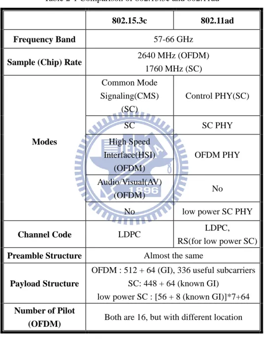
Both standards have OFDM and single carrier (SC) mode and have quite the same system specifications. The comparisons of these two standards are listed in Table 2-1[3]. In the 802.11ad, a new mode, named low power SC PHY, is added. This mode aimed to have low data rate with low power consumption. The low power SC mode uses Reed-Solomon (RS) code instead of low-density parity-check (LDPC) for channel coding to reduce the computational complexity and power consumption. Besides, the payload of this new mode is different with the other modes. The data block length is still 448 like the SC mode; however, it is divided into 7 sub-blocks which are composed of 56 data chips and 8 known data chips for GI. If single carrier frequency domain equalizer (SC-FDE) [6] is adopted in the receiver, a smaller sub-block length will reduce the power consumption. It is because frequency domain
equalizer needs less tap to equalize the received signals.
The following sections will focus on system specifications of IEEE 802.15.3c, since the final version of IEEE 802.11ad is not yet released.
Table 2-1 Comparison of 802.15.3c and 802.11ad
802.15.3c 802.11ad Frequency Band 57-66 GHz
Sample (Chip) Rate 2640 MHz (OFDM)
1760 MHz (SC) Modes Common Mode Signaling(CMS) (SC) Control PHY(SC) SC SC PHY High Speed Interface(HSI) (OFDM) OFDM PHY Audio/Visual(AV) (OFDM) No
No low power SC PHY
Channel Code LDPC LDPC, RS(for low power SC)
Preamble Structure Almost the same
Payload Structure
OFDM : 512 + 64 (GI), 336 useful subcarriers SC: 448 + 64 (known GI)
low power SC : [56 + 8 (known GI)]*7+64
Number of Pilot
2.2 IEEE 802.15.3c Specifications
The IEEE 802.15.3c standard which is based on SC and OFDM transmission is developed for Wireless Personal Area Network (WPAN) to provide short range (<10 m) and very high speed (>2 Gbps) multimedia data services to personal computer and consumer appliances located in rooms, offices, and so on [7]. In the beginning of transmission, IEEE 802.15.3c uses Common Mode Signaling (CMS) and a preamble is attached in front of the data stream. The CMS is specified to enable interoperability among different PHY modes. After the CMS, the frame payload is transmitted in different PHY modes. The preamble is added to aid receiver algorithms related to AGC setting, antenna diversity selection, timing acquisition, frequency offset estimation, frame synchronization, and channel estimation. With insertion of CP, it can reduce the impact of ISI. With channel coding, the system can correct the transmission errors. Furthermore, the standard defines interleaving, scrambler, unequal channel coding, and several modulation scheme to achieve better performance.
2.2.1 Basic Specifications
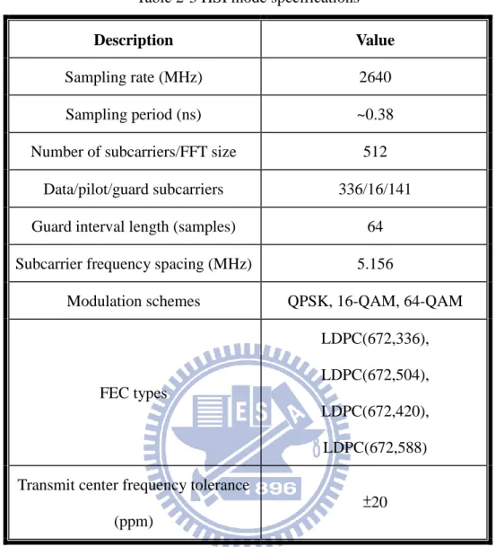
In IEEE 802.15.3c, there are three transmission modes: Single Carrier (SC) mode, High Speed Interface (HSI) mode, and Audio/Visual (AV) mode. HSI and AV mode use OFDM transmission, and SC mode is single carrier transmission. The detail specifications of SC and HSI mode are listed in Table 2-2 and Table 2-3 respectively.
The RF band occupies 9 GHz bandwidth while the sampling rate is 1760 MHz as shown in Fig. 2-1. The standard indicates that the RF band is divided into four sub-bands such that the Nyquist bandwidth of each sub-band is exactly 1760MHz. In
addition, each sub-band has 432 MHz spacing to prevent the interference from each other. In this case, the RF band can support 4 transmission bands without any interference. 65.88 GHz 63.72 61.56 59.40 57.24 CHNL #1 CHNL #2 CHNL #3 CHNL #4
Fig. 2-1 RF band plan Table 2-2 SC mode specifications
Description Value
Chip rate (MHz) 1760
Chip duration (ns) ~0.568 Subblock length (samples) 512
Pilot length (samples) 0 8 64 Length of data chips per subblock
(samples) 512 56 448 Modulation schemes π/2 BPSK, π/2 QPSK, π/2 8-PSK, π/2 16-QAM FEC types RS(255,239), LDPC(672,336), LDPC(672,504), LDPC(672,588), LDPC(1440,1344) Transmit center frequency tolerance
(ppm)
±25 Required frame error rate (FER)* 8 %
*: FER is determined at the PHY Service Access Point interface after any applied error correction methods. The measurement shall be performed in AWGN channel with a frame payload length of 2048
Table 2-3 HSI mode specifications
Description Value
Sampling rate (MHz) 2640 Sampling period (ns) ~0.38 Number of subcarriers/FFT size 512
Data/pilot/guard subcarriers 336/16/141 Guard interval length (samples) 64 Subcarrier frequency spacing (MHz) 5.156
Modulation schemes QPSK, 16-QAM, 64-QAM
FEC types
LDPC(672,336), LDPC(672,504), LDPC(672,420), LDPC(672,588) Transmit center frequency tolerance
(ppm)
±20
2.2.2 Equalization Related Specifications
In this standard, there are some well-known data streams that are assigned to specify different purposes, i.e. MAC layer control signal, the piconet coordinate signal, or the performance improving signal. This section will introduce the specific signaling that is directly related to the equalization.
Common Mode Signaling(CMS)
The CMS is a low data rate SC mode and specified to enable the switching among different PHY modes. It’s also used for transmission of the beacon frame, sync frame,
command frame, and training frame in the beamforming procedure. The order of sequences in time is SYNC, SFD and CES.
SYNC b128(48 repetition) SFD b128b128b128b128b128b128b128 CES b128b256a256b256a256a128
CMS
Time
Fig. 2-2 CMS frame format
As shown in Fig. 2-2, the CMS preamble is constructed by Golay complimentary sequences a128 and b128 of length 128, which are listed in Table 2-4. The SYNC field
uses a repetition of codes for higher robustness frame detection. The main purpose of SFD is used to establish frame timing as well as the header rate. The CES field is used for channel estimation. The sequences a256 and b256 inside the CES steam also hold
the property of Golay complimentary, and can be decomposed as
256 128 128 256 128 128 a [b a ] b [b a ] (2.1)
, where b128 and b128 in the sequences are transmitted first in time and the binary-complement of a sequence
x
is donated as x.Table 2-4 Golay sequences
Sequence name Sequence value
a128 0536635005C963AFFAC99CAF05C963AF
SC and HSI PHY preamble
A PHY preamble is added to aid the receiver algorithms such as AGC setting, timing acquisition, frame synchronization, and channel estimation. After the CMS, the system will switch to the designated mode and begin to transmit the data payload. In each beginning of transmission, the transmitter will send a PHY preamble to aid the receiver algorithms, just like the one in CMS. In SC mode, the preamble is transmitted at the rate of 1760 MHz. The SC PHY frame format and preamble structure are shown in Fig. 2-3 and Fig. 2-4.
Time
PHY preamble
PHY Payload field
Frame header
Fig. 2-3 SC PHY frame format
SC PHY preamble
SYNC a128(14 repetition) SFD MR[a128a128a128a128] HR[a128a128a128a128] CES b128b256a256b256a256Fig. 2-4 SC PHY preamble structure
Like CMS preamble structure, the PHY preamble consists of SYNC, SFD, and CES field. Each of the field functions like the one in CMS preamble: SYNC field for frame detection, SFD field for validating the beginning of the frame, and CES field for channel estimation.
The preamble of HSI mode is transmitted at the sampling rate of 2640 MHz. Two types of preamble are defined for this mode: the long preamble and optional short preamble. The former has the same structure as the CMS, and the latter has the same
structure as defined for the SC mode.
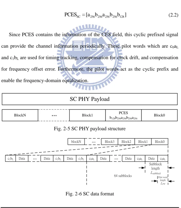
Data Payload and Pilot Channel Estimation Sequence(PCES)
In SC mode, the data stream is divided into data blocks with each data block has 64 sub-blocks, as shown in Fig. 2-5 and Fig. 2-6. Each data block is followed by a PCES. The PCES insertion is an optional feature that allows the system to re-acquire the channel information periodically. The PCES is the same as the CES field in the SC PHY preamble and is shown in (2.2).
SC 256 256 256 256 128
PCES = [a b a b b ] (2.2)
Since PCES contains the information of the CES field, this cyclic prefixed signal can provide the channel information periodically. These pilot words which are c0aL
and c1bL are used for timing tracking, compensation for clock drift, and compensation
for frequency offset error. Furthermore, the pilot words act as the cyclic prefix and enable the frequency-domain equalization.
SC PHY Payload
Block0 PCES
b128b256a256b256a256
BlockN
...
Block1Fig. 2-5 SC PHY payload structure
Block0 c0aL Data c0aL Data c0aL Subblock length Lsubblock Pilot word length LPW 64 subblocks Block1
blockN ... Block3 Block2
...
Data c1bL Data ... Data c1bL Data c1bL
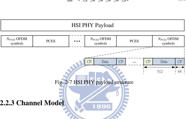
In HSI mode, every 96 (NPCES) OFDM symbols will insert one PCES, as shown in
Fig. 2-7. In one OFDM symbol, cyclic prefix of 64 samples is added to prevent ISI effect. The PCES is identical to the CES field prepended by a128 in the PHY preamble
which is shown in (2.3).
HSI 128 256 256 256 256 128
PCES = [a a b a b b ] (2.3)
HSI PHY Payload
NPCES OFDM symbols PCES NPCES OFDM symbols NPCES OFDM symbols
...
Data CP ... Data CP CP 512 64 CP PCESFig. 2-7 HSI PHY payload structure
2.2.3 Channel Model
Under the 60 GHz RF band, there are some special properties when waves are transmitted in the air that is much different from those below 10GHz RF band channel. Due to strong directivity, wave reflexes, diffracts, and scatters slightly. Also, the energy of the wave centralizes in a certain angles. Since the oxygen absorbs the wave in this RF band, the transmission distance is very short, less than 10 meters, which leads to negligible multipath effect. Based on these properties, IEEE 802.15.3c standard is pronounced for the indoor, over Gbps data rate wireless transmission using 60 GHz RF band. In general, for such a high data rate, the channel would be influenced a lot by line-of-sight (LOS)/non-light-of-sight (NLOS) channel, root-mean-square (RMS) delay spread, Doppler Effect, and negligible multipath effect when the wireless communication system operates under the 60 GHz RF band. These
properties are listed below: High Path Loss
While the EM wave passes through the medium, the medium absorbs the energy and limits the distance that the EM wave can travel. The more energy it lost, the shorter it can travel. The ratio of energy loss is mainly depends on the characteristic of the medium and the EM wavelength. The wavelength of 60 GHz wave is close to the length of the oxygen chemical bond, so the wireless communication in 60 GHz RF band suffers tremendously high path loss. As the result, the transmission distance is limited to about 10 m in maximum. Moreover, the effect of the multi-path fading is reduced since the non-line-of-sight (NLOS) wave travels more distance and loses more energy than the line-of-sight (LOS) wave.
Strong Directivity
The strong directivity means that the EM wave energy almost centralizes in a small angle path. Based on physical principle of diffraction, the beam width is inversely proportional to the operating frequency [8]. This phenomenon shows that the antenna can only receive the signal from the transmitter antenna within a small angle range. In conclusion, the NLOS path has lower path gain relative to the LOS path, and the multi-path fading effect is small.
The channel model is based on the golden set released by IEEE 802.15.3c group [9] [10]. The golden channel with RMS delay spread 3.2ns is chosen as the simulation channel model. Fig. 2-8 and Fig. 2-10 are SC channel impulse response and channel frequency response with sampling rate 1.76GHz, respectively. Fig. 2-9 and Fig. 2-11 are HSI channel impulse response and channel frequency response with sampling rate
2.64GHz, respectively.
Fig. 2-8 SC channel impulse response
Fig. 2-10 SC channel frequency response
Chapter 3
SC/OFDM Dual-Mode Frequency and
Time Domain Equalizer
This chapter will review frequency and time domain equalization with channel estimation in Section 3.1 and 3.2 respectively. Section 3.3 is the proposed frequency and time domain equalizer.
3.1 Review of Frequency Domain Equalization (FDE) [11]
A simple illustration of fully parallel FDE is shown in Fig. 3-1. The input passes through Serial-to-Parallel block and transforms to frequency domain by FFT. Then, the frequency domain data is multiplied with coefficients W and then transformed back to time domain by IFFT. Unlike TDE, the number of coefficients in FDE is fixed without regard to the length of the channel impulse response. The potential problem is when the length of the CIR is longer than the length of the CP. In that case, the circular convolution is ruined and FDE fails to equalize the channel effect. However, the channel model shows that the maximum length of CIR is far less than the length of CP, so this system does not have each problem.
FFT IFFT * * * … … … S/P P/S W0 W1 W511 input output
Fig. 3-1 Structure of fully parallel FDE
The formula of circular convolution can be transformed into a simple multiplication in the frequency domain, and the capital letter means frequency domain signal:
= Η
R D (3.1) ,where H is a diagonal matrix, R is a received signal vector, and D is transmitted data vector. To recover the transmitted data, we multiply the inverse of H on both sides of equation:
1 1
H R H H D D (3.2) , where the inverse of H is also a diagonal matrix. After CP removal, we can fully recover the transmitted signal D.
The above equations describe the ideal case: no AWGN and time-variant channel. In reality, the white noise always exists due to the thermal noise, and the channel varies with time due to many effects, such as related movement, air flow, or moving object. Thus, the equation should be:
( )
k Jk t Hk k k
, where Jk(t) means the time-variant effect matrix, Nk is a AWGN vector, and k is the
index of the subchannels. If we simply multiply the inverse of Hk all the time, the
time-variant effect will corrupt the data. Furthermore, to get the accurate inverse of Hk
is a difficult job under AWGN. To break through the predicament, the first thing is to overcome AWGN and get the inverse of Hk as accurate as possible. Then, an adaptive
algorithm is performed to track the changes in the time-variant channel. In this way, the time-variant component Jk(t) is no more an issue in the equalization.
3.1.1 Channel Estimation
In the beginning of the transmission, the transmitter sends the time-domain training sequence a256b256 (=u512) located in CES field to assist the equalization as
shown in Fig. 2-4. With the training sequence, we can easily estimate the channel matrix Hk, which is the inverse of the coefficients Wk.
512, U k k k H R (3.4)
,where U512 is the frequency domain constant value of u512, and k is the sub-carrier
index.
This solution is known as zero-forcing (ZF) method. The benefit is the simple implementation, but this method suffers from a problem: noise enhancement. With AWGN, Eqn. (3.4) is revised as Eqn. (3.5).
512, 512, U U k k k k k W H N (3.5)
The noise enhancement occurs when the channel gain Hk is so small that the noise
estimation result is far away from perfect estimation.
Since there are 2 U512 in CES, using Least-Square (LS) method is a better way
than using ZF. The main point of LS is to minimize the sum of the squares of the error. First of all, the equalization can be described as:
512, U k k k W R (3.6)
Second, apply the error
i caused by AWGN, where i stands for i-th U512 in CES.512, , , 512, , , U U k i k i i k k i i k i k W W R R (3.7)
Then, we need to minimize the sum of the squares, so let the partial derivative on
Wk be zero. 512, , 2 2 , 2 512, , 512, , ˆ , 2 3 U ( ) U U (2 2 ) 0 k i i k i i i k k i k i k i i k k k S W S
W W W W R R (3.8)Finally, the solution of ˆW indicates the system will have minimum of S. k
2 512, , , 512, , U ˆ ( U ) k i i k k i k i i
W R (3.9)Since there are 2 U512 (i=2) in CES and U512 is constant all the time, it can be
2 512, 512, 512, , 512, , ,1 ,2 2U U U ˆ 1 1 ( )U ) 2 2 k k k k k i k k i k k i i
W R R (R R (3.10)Substituting Rk with U512, the channel estimation result is:
512, 512, , 512, ,1 512, ,2 512, U U ˆ 1 ( U ) 1 ( U U ) 2 2 k k k k i k k k k k k i
W H N H H (3.11)With the summation of Nk, the noise enhancement is reduced since the mean of
AWGN is zero.
3.1.2 Adaptive Equalization
In OFDM system, pilot subcarriers are designed to indicate the changes of the time-variant channel. However, we do not have any known message in the frequency domain when the system is SCBT. Thus, our FDE requires an adaptive algorithm against the time-variant channel.
There are many adaptive algorithms developed in the literals. These algorithms mainly focus on their computational complexity and convergence speed. The widely used algorithms are Minimum-Mean-Square-Error (MMSE), Recursive-Least-Square (RLS), and Least-Mean-Square (LMS) [12],[13]. Due to 2640MHz sampling rate, high computational complexity algorithms are not suitable for such high sampling rate system because of high hardware complexity and power consumption. Furthermore, using the information of SNR is not practical in the hardware design. Based on above the considerations, we will show that LMS is a good choice for the FDE.
Let’s consider the block diagram of the adaptive FDE shown in Fig. 3-2. R is the output from FFT, and the adaptive FDE do the equalization and update filter
coefficients W. The FDE output is transformed back to time domain and decision of data is made by the demapper. The error E is the difference between FDE output and the training sequence (or sliced output when the data is transmitted).
Update
Channel
Coefficient
Adaptive
FDE
R
+
FDE output
Sliced output
Training sequence
W
-+
E
Fig. 3-2 Illustration of adaptive FDE
The idea of LMS algorithm is to use the method of the steepest descent to find a set of W which minimizes the cost function. In our design, the FDE takes a subblock into the equalization, so the cost function should involve a block of errors, which is so called Block LMS (BLMS) [14]. However, since the equalization is independent of each subchannel, we can consider each cost function Ck in each subchannel
independently instead of whole subblock.
2
{ }
k k
C Ex E (3.12)
The notation of Ex{.} is used to denote the expect value because we don’t want to be confused with the error E. Then, applying the steepest descent is to take the partial derivative with respect to the filter coefficients W.
* *
{ } 2 { }
C Ex Ex
EE EE (3.13)
zeros when the error E and coefficient W are in different subchannel. Then, substituting E with received signal R, we can rewrite Eqn. (3.13) as
* ( ) 2 { } k k k k k k k k k k k d d d d dC Ex d W W W W E D R R R E (3.14)
, where k is the subchannel index. Now, these derivatives show the steepest ascent of the cost function. To find out the minimum of the cost function, we take a step size of
2
in the opposite direction of the derivatives.
, * , 1 , , , { } 2 k n k n k n k n k k k n dC Ex d W W W W R E (3.15)
, where n indicates the subblock index or symbol index at SC or OFDM mode.
The expected value can be simplified, and the whole LMS algorithm can be expressed as:
LMS: *
, 1 ,
k n k n k k
W W R E (3.16)
The derivations of MMSE and RLS can be found in [16], [17]: MMSE: * 2 * 2 k k n k k s H W H H (3.17) RLS: * 1 1 n n n n n W P W W Y R U Y g U YU g E (3.18)
, where n indicates the subblock index or symbol index at SC or OFDM mode, 2 n
and 2 s
are variance of noise and signal respectively, Y is equalized signal, U is the intermediate vector, and gn is the gain vector.
Compared with MMSE [15]-[17] and RLS [18], [19], the LMS algorithm has less computational complexity than RLS since there is only one multiplication for updating at each sub-channel. In hardware design, more operations on updating will cause a longer feedback latency. The latency will impact the performance since the coefficient of equalizer can not be updated immediately. In high sampling rate system, high computational operations will required more pipelined stages, thus the latency is much longer. Furthermore, the low computational complexity leads to low power consumption. The low power issue is more important in the modern SOC design. In that case, LMS also has the advantage of low power consumption property. On the other hand, MMSE also has less computational complexity than RLS, but it requires the information of SNR, which is hard to be evaluated since there are Doppler and channel Effect on the received signal. Although there are some algorithms [15]-[17] trying to do SNR evaluation, the result is still not reliable in the practical system. Based on these considerations, LMS is suitable for FDE in high sampling rate design and can also achieve the required bit error rate (BER) with LS channel estimation that will be mentioned in Section 3.3.2.
3.2 Review of Time Domain Equalizer (TDE)
The basic structure of the TDE is the FIR filter, which performs the convolution between data stream and the filter coefficients. A simple illustration of the FIR filter is shown in Fig. 3-3, which is known as Zero Forcing (ZF). A robust adaptive decision
3.1.2. The Least Mean-Square (LMS) equalizer coefficients updating method is chosen to minimize the mean-square error, instead of ZF [20].
……… D D ……… D * * * ∑ ……… input * W0 W1 W2 wn output
Fig. 3-3 FIR filter structure
However, the computational complexity of the convolution in both ZF and LMS is proportional to the length of the filter taps, which is determined by the length of the CIR. From the channel model in Fig. 2-8 and Fig. 2-9, the filter coefficients must satisfy the mathematical property in Eqn. (3.19).
* 1 0 0 0
h w (3.19)
Although the parallel architecture can increase the throughput of TDE, the complexity grows linearly with the number of coefficients.
3.2.1 Multi-path Interference Cancellation
Multi-path Interference Cancellation (MPIC) [21] method is an efficient way for suppressing Inter-path Interference (IPI). MPIC is composed of two parts. The first part is multi-path interference replica, and the second part is multi-path interference cancellation [22].
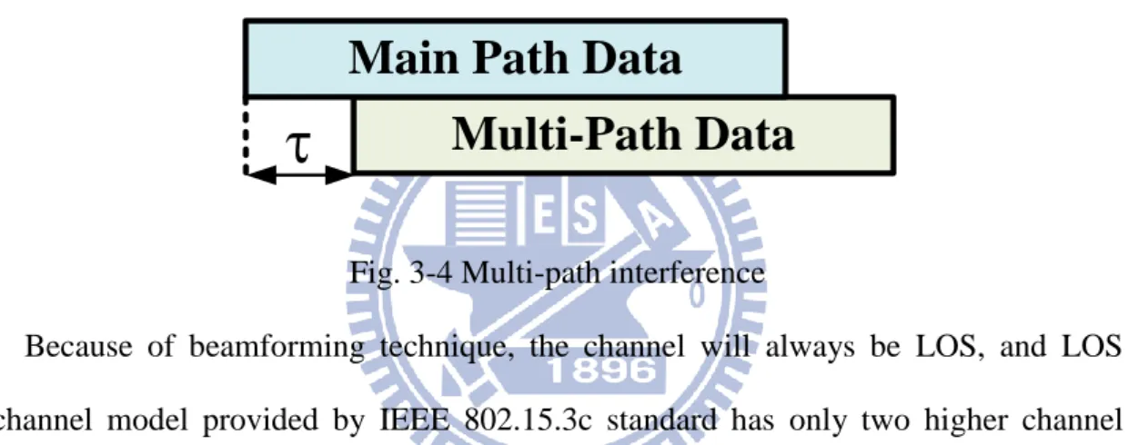
The following lower-case variables are all in time domain. In Fig. 3-4, during data transmission, dominant data path could be interfered by other multi-path data and is the multi-path delay.
Multi-Path Data
Main Path Data
Fig. 3-4 Multi-path interference
Because of beamforming technique, the channel will always be LOS, and LOS channel model provided by IEEE 802.15.3c standard has only two higher channel path gains. The rest channel path gains almost equal to zeros. Therefore, the received signal is expressed like
1,1 1,1 , , h 0 0 h 0 0 0 0 0 0 0 0 0 0 h 0 0 0 0 0 0 0 0 0 0 0 0 0 0 0 0 0 0 0 0 0 0 h N N N N h y x = x (3.20)
, where h means channel impulse response matrix, x is the transmitted data vector, and y is the received signal vector. Define main data path gain vector
1,1 2,2 , [ ]=[h h ... h ], 1, 2,..., [ ]=0 , 0 N N t t N t t h h (3.21)
and second data path gain vector
1,1+ 2,2+ - , [ ]=[h h ... h ], 1, 2,..., [ ]=0 , 0 N N t t N t t m m (3.22)
where N is the number of total sub-channels.
A modified MPIC [21] has two stages. In initial stage, we can obtain the channel impulse response after channel estimation. Assume multi-path gain is small, so we don’t consider the multi-path gain m[t]. Then, we have
[ ] ˆ[ ] , 1, 2,..., [ ] t t t N t y x h (3.23)
, where xˆ[ ]t is initial data vector without considering multi-path effect. Because the second path delay is , it means the dominant received signal will be affected by the second received signal after time . In update stage, the received signal cancels the second path interference and the result is divided by the main path gain to get the updated transmitted data x[t].
ˆ [ ] [ ] [ ] [ ] , 1, 2,..., [ ] t t t t t N t y m x x h (3.24)
The equation from (3.22) can be simplified as [ ] [ ] [ ] [ ] , 1, 2,..., [ ] t t t t t N t m x x x h . (3.25)
If we only consider about high channel path gain which interferes the received signal larger, it can reduce the hardware complexity of traditional time domain equalization. The filter taps won’t increase with the length of channel impulse response.
3.2.2 Golay-Sequence Aided Channel Estimation [15]
A set of complementary series is defined as a pair of equally long, finite sequences of two kinds of elements which have the property that the number of pairs of like elements with any one given separation in one series is equal to the number of pairs of unlike elements with the same given separation in the other series. For example, the two series a = 00010010 and b = 00011101 are complementary [23].
Golay Sequence Property
Golay sequences with N of length are generated by delay and weight vectors with M of each length and a recursive algorithm [24], [25]. Binary Golay sequences are generated when the delay vector D[D0...DM1] is chosen as any permutation of
0 1
[2 ...2M] and the weight vector W [W W0... M1] has 1 of elements. The recursive algorithm for generating Golay sequences is described as follows:
,(0)( ) ( ) N a i i , (3.26) ,(0)( ) ( ) N b i i , (3.27) ,( )( ) 1 ,( 1)( ) ,( 1)( 1) N m m N m N m m a i W a i b iD , (3.28) ,( )( ) 1 ,( 1)( ) ,( 1)( 1) N m m N m N m m b i W a i b iD , (3.29) ,(0)( ) ,(M)( ) N N a i a i , (3.30) ,(0)( ) ,(M)( ) N N b i b i . (3.31) Golay sequences are complementary sequences, which have an attractive property that the sum of their autocorrelations has single maximum peak and no side-lobe.
A pair of Golay sequences for i0,...,N1, with N 2M: ( )
Autocorrelation property: ( ) ( ) 2 ( ) a b R i R i N
i , (3.33) where 1 * 0 ( ) ( ) ( ) N i a N N k R i a k a k i
, (3.34) and 1 * 0 ( ) ( ) ( ) N i b N N k R i b k b k i
. (3.35) The symbol “*” denotes complex conjugate. Estimation Procedure
The received channel estimation sequence (CES) is expressed by
1 0 ( ) ( ) ( ) ( ) CH T CE CE t r t h t s t t n t
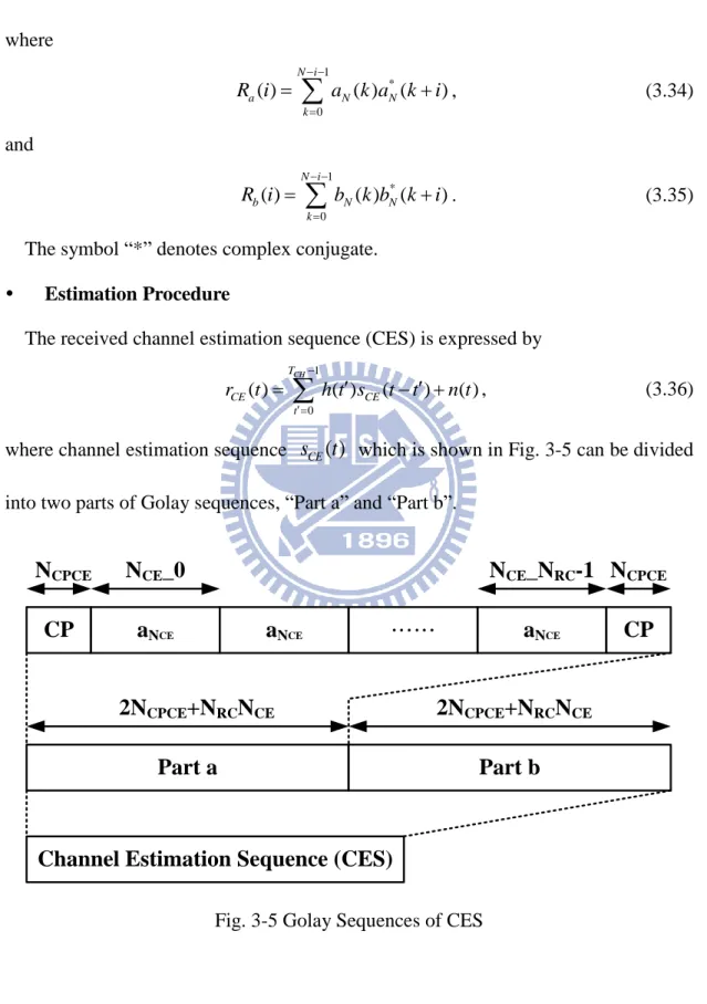
, (3.36) where channel estimation sequence sCE( )t which is shown in Fig. 3-5 can be divided into two parts of Golay sequences, “Part a” and “Part b”.Channel Estimation Sequence (CES)
Part a
Part b
CP
a
NCEa
NCE……
a
NCECP
N
CPCEN
CE_0
N
CE_N
RC-1 N
CPCE2N
CPCE+N
RCN
CE2N
CPCE+N
RCN
CEFig. 3-5 Golay Sequences of CES
sequences with length NCE and cyclic prefix and postfix with length NCPCE. The base
sequences for “Parts a and b” are Golay sequences ( )
CE N a i and ( ) CE N b i , respectively.
Then, the total length of CES is 2(2NCPCE + NRCENCE).
First, the Golay correlator calculates correlation values between the received CES and Golay sequences ( )t and ( )t :
1 * 0 1 ( ) ( 1) ( ) CE CE N CE CE N d CE t r t d N a d N
, (3.37) 1 * 0 1 ( ) ( 1) ( ) CE CE N CE CE N d CE t r t d N b d N
. (3.38)Then, CPs are removed from the correlation values:
ˆ( )t (t NCPCE),t 0,...,NRCENCE 1
, (3.39)ˆ( )t (t 3NCPCE NRCENCE),t 0,...,NRCENCE 1
. (3.40) After that, CIR h tˆ( ) is estimated by sum and average operations:
0 1 ˆ( ) ( (ˆ ) ˆ( )) 2 RCE N CE CE p RCE h t t pN t pN N
. (3.41)The derived noiseless channel impulse response can be used in MPIC equalization.
3.3 Proposed Architecture for IEEE 802.15.3c
3.3.1 Proposed Adaptive LS-LMS FDE [11]
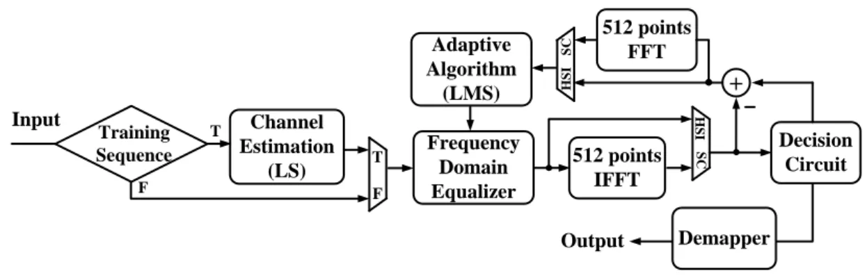
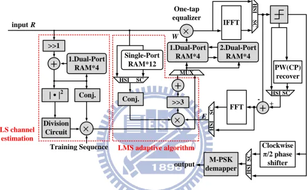
The proposed adaptive LS-LMS FDE operates based on equations in Section of 3.1.1, and 3.1.2, and the block diagram is shown in Fig. 3-6.
Frequency Domain Equalizer Channel Estimation (LS) Adaptive Algorithm (LMS) 512 points IFFT Decision Circuit Input Output 512 points FFT Demapper S C H S I S C H S I F T T F Training Sequence +
Fig. 3-6 Block diagram of the proposed adaptive LS-LMS FDE The pseudo code of the system flow is explained as followed:
1. If (received signals == training sequences) the LS channel estimation evaluates the channel coefficients, else the received signals will be equalized by FDE. 2. If (mode == SC) the equalized data will be transformed to time domain by IFFT
and sent to decision circuit, else will be sent to decision circuit straightly.
3. If (mode == SC) the errors between equalized and sliced signal will be transformed to frequency domain by FFT and sent to LMS adaptive algorithm, else will be sent to LMS adaptive algorithm straightly.
4. While (received signals == valid data) LMS adaptive algorithm will update the channel coefficients in FDE.
The proposed adaptive LS-LMS FDE needs additional two FFT (FFT and IFFT) for SC/OFDM dual mode system. In SC mode, the equalized signal must be transformed to time domain to do slicing, and the error between equalized data and decision data will be transformed back to frequency domain for adaptive algorithm. Although the hardware complexity is large, the adaptive LS-LMS FDE can track the change of time-variant channel.
LMS has to do training to achieve convergence before any data is ready to be equalized. To accelerate the convergence speed, a fast LMS algorithm is applied by simply increasing the step size [26]. However, compared with other algorithms, LMS still suffers the slow convergence speed problem [27]. Therefore, the training time of LMS is longer than others, and it requires longer training sequence to do training. According to the standard, the training sequence is available in CES field of PHY preamble. However, there are only two a256b256 for training before payload, so the
training result of LMS is not good enough as compared with LS channel estimation. The learning curves are shown in Fig. 3-7. The simulation is under the channel model which RMS delay is 3.2ns and SNR is 18 dB. LMS algorithm takes about extra12 data subblocks to achieve the same performance of LS-LMS combined algorithm. The result supports that the convergence speed of the combined algorithm is indeed faster than single LMS algorithm.
3.3.2 Proposed LOS Golay-MPIC TDE
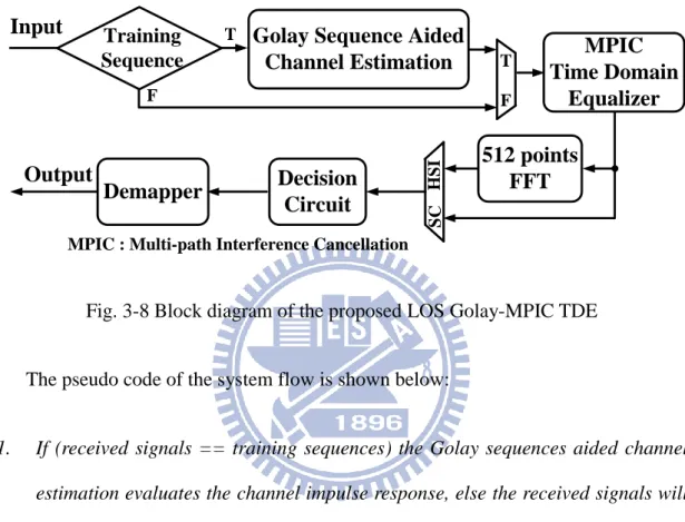
The proposed LOS Golay-MPIC TDE operates based on equations in Section of 3.2.1 and 3.2.2, and the block diagram is shown in Fig. 3-8.
MPIC Time Domain Equalizer 512 points FFT Decision Circuit Output Demapper S C H S I
Golay Sequence Aided Channel Estimation Input F T T F Training Sequence
MPIC : Multi-path Interference Cancellation
Fig. 3-8 Block diagram of the proposed LOS Golay-MPIC TDE The pseudo code of the system flow is shown below:
1. If (received signals == training sequences) the Golay sequences aided channel estimation evaluates the channel impulse response, else the received signals will be equalized by MPIC TDE.
2. If (mode == HSI) the equalized data will be transformed to frequency domain by FFT, else will go through next block straightly.
3. While (received signals == valid data) the equalized data will be sent to decision circuit and demapper.
The proposed LOS Golay-MPIC TDE has low hardware complexity, which doesn’t need additional IFFT/FFT for SC/OFDM dual mode system. In each PCES period, the LOS Golay-MPIC TDE will update the channel impulse response again by Golay sequence aided channel estimation.
The LOS channel model provided by IEEE 802.15.3c standard has only two higher channel path gains. Also, the second path gain of LOS channel model is at most 0.3 and the other paths are less than the main path [9] [10]. Therefore the MPIC TDE can be efficiently implemented. For evaluating the influence of the multi-path gain and delay, different test patterns with AWGN and test channels are created. The test channels have one main path and one delayed path, and the second path gain and delay differs from 0.1 to 0.5 and differs from 8 to 56 samples which is normalized to main path, respectively. The modulations of SC and HSI mode are pi/2 QPSK and QPSK respectively. In Fig. 3-9 and Fig. 3-10, it shows BER is very sensitive to second path gain, but rarely affected by second path delay.
Fig. 3-10 BER of TDE HSI mode for 2 channel paths
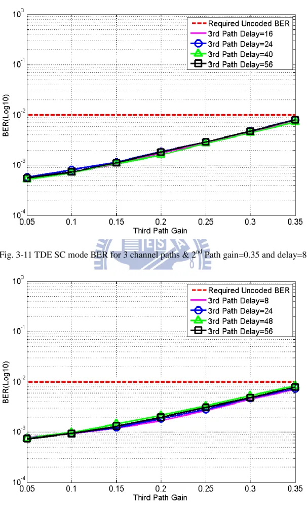
If the number of LOS channel paths has more than two paths, the proposed Golay-MPIC TDE can still work. But the BER will be worse as long as the third path gain becomes larger. Take SC mode with three channel paths as example, Fig. 3-9 shows the BER is 4.89*10-4 and 6.64*10-4 when the second path gain is 0.35 and delay is 8 and 40, respectively. If the third channel path is involving for these two cases, the BERs are shown in Fig. 3-11 and Fig. 3-12. In Fig. 3-11 and Fig. 3-12, when the third path gain becomes small, the BER is near 4.89*10-4 and 6.64*10-4, respectively. The performance of different delay of the third path is almost the same.
The proposed LOS Golay-MPIC TDE can achieve the BER requirement of IEEE 802.15.3c standard. If the number of LOS channel paths is more, the computation is more complex. Also, the number of register becomes more with the longer delay path. Therefore, we consider the general case of two higher gain channels. It can reduce hardware complexity and achieve the required BER. Section 4.2.1 will describe an efficient architecture design of Golay-sequence aided channel estimation.
Chapter 4
Architecture Design and Performance
Analysis
This chapter describes architecture design of the proposed adaptive LS-LMS FDE and LOS MPIC TDE in Section 4.1. The detail sub-blocks design is shown in Section 4.2. Section 4.3 is the synthesis result and performance of the proposed adaptive LS-LMS FDE and LOS MPIC TDE. The comparison of the proposed adaptive LS-LMS FDE and LOS MPIC TDE is presented in Section 4.4
4.1 Design Specifications and Architecture
IEEE 802.15.3c and IEEE 802.11ad standards focus on over Gbps data rate wireless communication. To achieve the target, there are two key features in the standard. The first one is the usage of the 60 GHz RF band. The unlicensed RF bandwidth is wide enough to support the usage of large bandwidth. The transmission rate is proportional to the bandwidth, so using the unlicensed 60 GHz RF band is essential. The second one is the ultra-high sampling rate. Although there are many methods to achieve the target of high data rate, like using higher modulation or multi-input and multi-output (MIMO) system [28], raising the sampling rate is the most direct way since the data rate is proportional to the sampling rate. With the moderate modulation scheme, the data rate could be twice or three times of the sampling rate. In this way, we can easily achieve the target of over Gbps data rate.
In modern CMOS process, the issue of power consumption becomes more and more important. There are many methods to reduce the power consumption when we design the hardware, such as using low computational complexity algorithm, substituting high complexity arithmetic unit with lower one, or sharing the hardware resources. By using these methods, we can reduce the chip area and the switching power consumption. Meanwhile, the leakage power is also reduced when the chip area is reduced.
As identical in Section 2.2.1, the sampling rate is 1760 MHz in SC mode and 2640 MHz in HSI mode. In the hardware design, this fact means the throughput of the chip is also 2640 MHz for dual mode system. There are two ways to fulfill the requirement: pipeline or parallel structure.
The pipeline structure is essential for such high computational and high speed digital circuit. Although inserting more flip-flops can reduce the operating time in one stage and increase the clock rate, the cost is large chip area due to large number of flip-flops. Moreover, there is insertion delay (tsetup + tC-Q) of the flip-flops, where tsetup
and tC-Q are the setup and clock to Q delay time of flip-flops. Thus when clock rate is
very high and computation path is long, the fully pipelined structure is not a good design. Using the parallel structure can reduce the clock rate and maintain the throughput at the same time. The drawback is the area is proportional to the number of the copies. Although the slower clock rate leads to lower power consumption, too many copies will generate more leakage power than expected, which violates our purpose of low power design.
Based on the considerations above, we adopt the combined structure. The system parameters are listed in Table 4-1. For dual mode system, we set the clock rate at 330 MHz with 8 parallels, based on two considerations: the clock rate and the power consumption.
Table 4-1 System parameters
SC HSI Sampling rate (MHz) 1760 2640 Clock rate (MHz) 220 330 Modulation π/2 QPSK QPSK FFT point/sub-block length 512 symbols CP length 64 symbols Channel model
LOS residual model [9] RMS delay spread: 3.2 ns
Max. data rate (uncoded)
3.52 Gbps 5.28 Gbps
4.1.1 Proposed Adaptive LS-LMS FDE and Baseband
Receiver [11]
FFT FDE Value of correlation 8x data from ADC [9:0] FCFO Estimation CORDIC 1~8x phase 8x data from SCO [9:0] ‧ ‧ ‧ ‧ ‧ ‧ 8x de-rotated data [9:0] ‧‧‧ ‧ ‧ ‧ 8x data from FFT [13:0] ‧ ‧ ‧ 8x data from CE [12:0] [5:0] De-rotator 8x CORDIC ‧‧‧ SCO Interpolator ACC ‧‧‧ NCO EstimatedCFO phase Boundary *22/375 >>22 *33/375 >>22 ‧‧‧ SCO ppm CFO Tracking PD & BD & CFO detection Hard Demapper 8x data out [5:0] ‧‧‧
Fig. 4-1 Proposed block diagram of baseband receiver design
The baseband receiver mainly consists of three blocks which is shown in Fig. 4-1. The first block is the synchronization block, which consists of SCO compensator, symbol boundary detection (BD), and CFO synchronization. SCO performs the time interpolation method and the frequency rotation method for the dual modes. Symbol boundary detection (BD) allocates the incoming packet and finds the symbol boundary located in the ISI free region. CFO synchronization which uses correlation based method to estimate FCFO and can be realized by the same hardware with symbol synchronization. The second block is the FFT and frequency domain equalizer (FDE). FFT transforms signals from time domain into frequency domain, and FDE eliminates the channel effect. The final block is the LDPC decoder that corrects the error bits using normalized min-sum algorithm with row-based layered scheduling and can support four code rates of 802.15.3c applications.
The proposed LS channel estimation combined LMS FDE has been described in Section 3.2.1. The block diagram shown in Fig. 3-6 is redrawn in Fig. 4-2 due to the hardware design considerations. In the following sections, we will discuss our hardware design. FFT and IFFT are not the design target in this thesis and is implemented by[29]. R Training Sequence W -+ E LS channel estimation One-tap equalizer input M-PSK demapper Clockwise π/2 phase shifter PW(CP) recover output LMS adaptive algorithm 1.Dual-Port RAM*4 1.Dual-Port RAM*4 2.Dual-Port RAM*4 Single-Port RAM*12 H S I S C Conj. >>1
+
| • |2 Division Circuit
+
+
Conj. >>3 MUX HSI SC H S I S C IFFT FFT HSI SC H S I S CFig. 4-2 Block diagram of the proposed adaptive LS-LMS FDE
The proposed LS-LMS FDE can be used on SC and HSI mode in IEEE 802.15.3c specification. Fig. 4-2 shows SC and HSI mode system architecture. The signals flows of SC and HSI mode are different at FFT feedback loop, The SC mode needs to transform to time domain to obtain the original data. After doing slicing, the errors will be transformed to frequency domain to do LMS algorithm. SC mode has additional feedback delay, so it needs single-port memories to save the received data for feedback FFT output. The complex multiplier (|.|2) in LS can be shared in one-tap equalizer, and the complex conjugate multiplier (Conj.) in LS can also be shared in LMS. Besides, in Fig. 4-2, the four dual-port memories marked with “No.1” in LS