Formation of dual-phase Hf O 2 – Hf x Si 1 x O 2 dielectric and its application in
memory devices
Ying Qian Wang, Jing Hao Chen, Won Jong Yoo, Yee-Chia Yeo, Albert Chin, and An Yan Du
Citation: Journal of Applied Physics 98, 013536 (2005); doi: 10.1063/1.1954870 View online: http://dx.doi.org/10.1063/1.1954870
View Table of Contents: http://scitation.aip.org/content/aip/journal/jap/98/1?ver=pdfcov Published by the AIP Publishing
Articles you may be interested in
Investigation of local charged defects within high-temperature annealed Hf Si O N Si O 2 gate stacks by scanning capacitance spectroscopy
J. Appl. Phys. 101, 083704 (2007); 10.1063/1.2717600
Pd-nanocrystal-based nonvolatile memory structures with asymmetric Si O 2 Hf O 2 tunnel barrier Appl. Phys. Lett. 89, 083109 (2006); 10.1063/1.2335677
Multibit memories using a structure of Si O 2 /partially oxidized amorphous Si Hf O 2 Appl. Phys. Lett. 89, 033122 (2006); 10.1063/1.2219999
In situ low-angle x-ray scattering study of phase separation in initially mixed Hf O 2 – Si O 2 thin film interfaces Appl. Phys. Lett. 85, 5884 (2004); 10.1063/1.1831554
Surface potential and morphology issues of annealed ( HfO 2 ) x ( SiO 2 ) 1x gate oxides J. Vac. Sci. Technol. B 22, 2113 (2004); 10.1116/1.1771673
An Yan Du
Institute of Microelectronics, 11 Science Park Road, Singapore Science Park II, Singapore 117685
共Received 28 January 2005; accepted 20 May 2005; published online 13 July 2005兲
In this paper, we studied the phase-separation phenomenon of Hf0.5Si0.5O2film deposited on SiO2
or sandwiched by SiO2, by x-ray photoelectron spectroscopy and transmission electron microscopy.
The Hf0.5Si0.5O2 film underwent phase separation to form a doublet-phase HfO2– HfxSi1−xO2 共x
⬍0.5兲 film, and was used as a trapping layer in a metal-blocking oxide-silicon nitride-tunnel oxide-silicon-type memory structure, where the dual-phase HfO2– HfxSi1−xO2 共DPHSO兲 film
replaces the conventional silicon nitride共Si3N4兲 trapping layer. The charge storage properties of the
DPHSO film were investigated and compared with HfO2 and Si3N4. It was found that for a given electric field applied to the tunnel oxide, the programming speed of memory devices using a DPHSO or HfO2 film as a trapping layer is faster than that using Si3N4. This indicates the higher
electron-capture efficiency of the DPHSO and HfO2 films. In addition, the double-phase
microstructure of the DPHSO film also provided better retention property than pure HfO2. © 2005 American Institute of Physics.关DOI: 10.1063/1.1954870兴
I. INTRODUCTION
The polycrystalline silicon- or metal-oxide-nitride-oxide-silicon共SONOS or MONOS, respectively兲 nonvolatile memory structure has received considerable attention for ap-plication in electrically erasable and programmable read only memory 共EEPROM兲 devices.1–3 The attractiveness of the MONOS flash memory, compared to the current commercial floating gate memory, lies in its low programming/erasing voltage, immunity to drain-induced turn on,4 and improved retention and endurance properties because the local defect-related charge leakage can be significantly reduced.2,3 Re-cently, materials such as high-permittivity 共high k兲 dielec-trics, e.g., Ta2O5, HfO2, and Al2O3, have been explored to replace silicon nitride in the SONOS or MONOS structure to improve both the programming and retention properties.1–3
Hafnium silicate dielectric film is an attractive trapping material in MONOS memory application due to its process compatibility with the conventional complementary metal-oxide semiconductor 共CMOS兲 process. In addition, hafnium silicate is known to undergo phase separation5–8 to form a crystalline hafnium oxide 共HfO2兲 phase and an
amorphous-silica-rich phase when annealed at temperatures above 900 ° C, giving rise to a unique microstructure comprising HfO2 nanocrystals that could be suitable for memory
appli-cations. Therefore, a memory device with a hafnium silicate trapping layer could combine the benefits of the MONOS
structure and the nanocrystal memory. Recently, Lin et al.9 demonstrated memory devices comprising HfO2dots formed
by the phase separation of the hafnium silicate film. In this article, we focus on the materials analysis of the dielectric stack in the memory device structure共silicate film deposited on SiO2or sandwiched by SiO2兲 because the top and bottom
SiO2may impact the thermal stability of the silicate film. We
also provided experimental comparison of the trapping prop-erties of the dual-phase HfO2– HfxSi1−xO2 共DPHSO兲 film
with those of the HfO2 and Si3N4 films in MONOS-type
memories, in order to better evaluate the advantage of each material in MONOS-type memory applications. The pro-gramming and retention properties are also compared. The relation between the device performance and material prop-erty is analyzed.
II. DEVICE FABRICATION
Memory devices with the TaN / SiO2/ X / SiO2/ Si struc-ture were fabricated, where X represents the charge-trapping layer which can be DPHSO, HfO2, or Si3N4. A schematic of the device structure is shown in Fig. 1. Tantalum nitride 共TaN兲 is selected as the gate material, instead of n+
polysili-con, because the midgap work function of TaN has been reported to contribute to an enlarged memory window by reducing electron injection from the gate through the block-ing oxide durblock-ing erase operation.10
P-type Si共100兲 substrates were used as the starting
ma-terials. After a standard pre-gate clean, a 4-nm-thick SiO2
tunnel oxide was grown by dry oxidation at a temperature of
a兲Electronic mail: [email protected]
b兲Author to whom correspondence should be addressed; electronic mail: [email protected]
0021-8979/2005/98共1兲/013536/5/$22.50 98, 013536-1 © 2005 American Institute of Physics
800 ° C. On one wafer, a Hf0.5Si0.5O2 film was deposited on
the SiO2 tunnel oxide by the cosputtering of Hf and Si
tar-gets in an argon and oxygen共Ar+O2兲 ambient at a pressure
of 3 mTorr. On the first control wafer, the HfO2 film was
formed on the tunnel oxide by reactive sputtering of a Hf target in the Ar+ O2ambient. On the second control wafer, a
Si3N4 film was formed on the tunnel oxide by sputtering Si
in an ambient containing argon and nitrogen. The thicknesses of the Hf0.5Si0.5O2, HfO2, and Si3N4films were controlled by
adjusting the sputter-deposition rate. The physical thick-nesses of the Hf0.5Si0.5O2, HfO2, and Si3N4 charge-trapping
layers共Fig. 1兲 were measured by an ellipsometer and a pro-filer. The thicknesses were different as no process optimiza-tion to match the thicknesses was made. Next, all the charge-trapping layers were capped with an 8-nm-thick SiO2which
was formed by low-pressure chemical vapor deposition 共LPCVD兲 using a Si共OC2H5兲4共TEOS兲 precursor at a
depo-sition temperature of 700 ° C. Subsequently, a 150-nm-thick TaN metal gate was formed by sputtering a Ta target in an Ar+ N2 ambient with a dc power of 450 W at a pressure of
3 mTorr, followed by gate patterning and etching. Finally, As+implantation and activation anneal at 1000 ° C were
per-formed to form the source/drain regions.
III. MATERIALS CHARACTERIZATION
X-ray photoelectron spectroscopy 共XPS兲 and transmis-sion electron microscopy共TEM兲 were utilized to investigate the material properties of the Hf0.5Si0.5O2 film, paying par-ticular attention to phase transformation and distribution.
The Hf0.5Si0.5O2film employed for XPS characterization was formed by the same process as that used for device fabrication. The Hf0.5Si0.5O2 film was then annealed at vari-ous temperatures in an inert ambient, and XPS was used to reveal the change of the chemical composition of the Hf0.5Si0.5O2 film as the anneal temperature increases. The
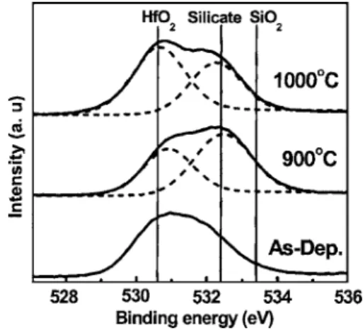
ratio of Hf and Si in the film was found to be 1:1 from compositional XPS analysis. Figure 2 shows the spectra of the O 1s core level of the Hf0.5Si0.5O2films as deposited and
after annealing at 900 and 1000 ° C. The O 1s binding ener-gies of SiO2 and HfO2 are 533.4 and 530.6 eV,
respectively,11 as indicated in Fig. 2. The O 1s binding en-ergy of an amorphous hafnium silicate with a composition of Hf6Si29O65 is about 532.4 eV,12and this is also indicated in
Fig. 2. Considering the fact that Zr and Hf have similar
elec-tronic configurations, one may refer to Ref. 13 for an inter-pretation of the XPS spectra. Reference 13 gives a detailed analysis of the XPS spectra shape and peak positions of Zr silicate films. In our experiment, the difference between the XPS spectra of as-deposited samples and samples annealed at high temperatures confirms phase separation, showing two types of chemical composites in the annealed Hf0.5Si0.5O2
films. By fitting the XPS spectra using two Gaussian profiles as shown in Fig. 2, it is determined that the two components in the annealed 共900 or 1000 °C兲 samples are HfO2 and
hafnium silicate. The difference between the 900 and 1000 ° C annealed samples is that the ratio of O atoms asso-ciated with HfO2 is larger in the 1000 ° C annealed sample,
indicating further phase separation of Hf0.5Si0.5O2 film at
1000 ° C. Hence, the XPS study reveals HfO2and silica-rich
Hf silicate phases in the Hf0.5Si0.5O2 film after
high-temperature annealing.
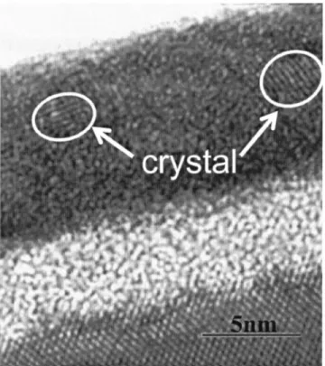
A cross-sectional TEM picture of a SiO2/ Hf0.5Si0.5O2/ SiO2 sandwich structure annealed at
900 ° C is shown in Fig. 3. Microstructures showing crystal-line phases embedded in an amorphous matrix are clearly observed. The size of the crystals is in the range of 5 – 10 nm. Since the kinetic-energy barrier needed to form a crystalline hafnium silicate is large, the crystalline silicate phase can never be observed under normal annealing conditions,5–8 thus we believe that the crystals in Fig. 3 should be HfO2. In addition, the lattice constant measured from TEM is about 0.31 nm, which is close to the 共111兲 lattice constant of a monoclinic HfO2 crystal. The amorphous phase in Fig. 3 is considered to be a hafnium silicate matrix with a significant brightness contrast from that of the underlying SiO2. For the
sample which was annealed at 1000 ° C, two phases were also observed in the trapping layer by TEM, but the size of the crystals is larger than that observed in the sample an-nealed at 900 ° C, and the brightness constrast between the amorphous phase and the underlying SiO2 layer is also
lower. This indicates that further phase separation had oc-curred with annealing at a higher temperature.
The XPS and TEM analyses consistently indicate that the following reaction occurred when the Hf0.5Si0.5O2 film
was annealed at high temperatures:
FIG. 1. Schematic diagram showing the cross section of the memory device. The inset shows the thicknesses of the trapping layer and the capacitance effective thickness共teff兲 of the entire dielectric stack which is calculated for the accumulation regime.
FIG. 2. XPS spectra showing the O 1s core level of the as-deposited 共As-Dep.兲 Hf0.5Si0.5O2 film after annealing at 900 and 1000 ° C. High-temperature anneal leads to the formation of two phases, including the HfO2 phase and the Hf-silicate phase.
013536-2 Wang et al. J. Appl. Phys. 98, 013536共2005兲
Hf0.5Si0.5O2→
0.5 − x 1 − x HfO2+
0.5
1 − xHfxSi1−xO2,
where 0⬍x⬍0.5. Lin et al. reported a phase separation of HfxSi1−xO2 into crystalline HfO2 and amorphous SiO2,9
which can be expressed by HfxSi1−xO2→xHfO2+共1
− x兲SiO2, where the HfxSi1−xO2film was in contact with the
Si substrate. Their different observations from the results of this work could be due to the different initial material com-positions or the different layer structures employed in mate-rials characterization.
IV. MEMORY OPERATION AND RESULTS DISCUSSION A. Memory effect and programming characteristics
Figure 4共a兲 shows the memory effect of a MONOS-type device employing Hf0.5Si0.5O2as a trapping layer. Since the devices underwent a source-drain activation anneal at 1000 ° C, the Hf0.5Si0.5O2film has a DPHSO structure. After
applying a positive voltage pulse to the gate electrode while keeping the source, drain, and substrate terminals grounded, the threshold voltage 共Vth兲 shifts to a higher value since net
negative charge is injected from the Si substrate. The thresh-old voltage was determined by the intercept of a tangent of the Id-Vg curve共measured at Vds= 0.2 V兲 at the point where
the transconductance is the maximum. The threshold voltage as a function of stress time is shown in Fig. 4共b兲. According to the International Technology Roadmap for Semiconduc-tors 共ITRS兲 2004,14the requirement of memory window for non-volatile flash memory is larger than 3 V. In our device, 3 V can be attained by stressing at 15 V for 10 ms.
The programming properties of the device with the DPHSO trapping layer were compared with devices employ-ing HfO2 and Si3N4 trapping layers. It was found that the
devices with DPHSO and HfO2trapping layers offer higher programming speeds with lower programming voltages than the device with Si3N4 trapping layer.
Figure 1 lists the capacitance effective thickness 共teff兲,
which was calculated using teff= Aox/ Ceff,15where Ceffis the
capacitance obtained from the capacitance-voltage 共C-V兲 characteristics in the accumulation region,oxis the
permit-tivity of SiO2, and A is the gate area. The teffof the devices with HfO2 and DPHSO trapping layers are about the same, but smaller than that of the device with a Si3N4 trapping
layer. This is partly due to the higher dielectric constants of HfO2and HfxSi1−xO2. The electric field in the tunneling
ox-ide of the fresh device can be estimated by Eox=共Vg− Vfb
−s兲/teff,15where Eoxis the electric field in the tunnel oxide
and Vg, Vfb, andsare the applied gate voltage, the flatband
voltage, and the surface potential, respectively. Therefore, for a given electric field in the tunneling oxide, the applied gate voltage is smaller for the HfO2 and DPHSO devices
compared to the Si3N4 device.
Figure 5 compares the programming properties of the three devices, with a Vgof 14 V applied to the devices with
a HfO2 or DPHSO trapping layer, and 18 V applied to the
devices with a Si3N4 trapping layer. At this bias condition,
the value of Eoxis about 10 MV/ cm and electrons should be injected from the substrate to the trap layer via Fowler-Nordheim 共FN兲 tunneling, as illustrated in Fig. 6. The FN tunneling current density is given by JFN
= AEox2 exp共共−B/Eox兲兲, where Eoxis the electric field through
the tunneling oxide, and A and B are constants as given by
FIG. 3. TEM image of a SiO2/ Hf0.5Si0.5O2/ SiO2dielectric stack structure that was annealed at 900 ° C, revealing the microstructure of crystals em-bedded in an amorphous matrix.
FIG. 4.共a兲 Memory window and 共b兲 threshold voltage change as a function of programming time and programming voltage of the memory device with the dual-phase HfO2– HfxSi1−xO2共DPHSO兲 trapping layer.
A = q3共m/mox兲/8h⌽B and B = 8
冑
2mox⌽B 3/ 3qh.16 Hence the tunneling current is only determined by the electric field, and the injection current from substrate to trapping layer should be the same for all the three devices.
The programming speed was determined by d⌬Vth/ dt
=Jinj/ Cg,17 where is the capture efficiency, Jinj is the
injection current, Cgis the capacitance between a centroid of
a trapped charge and the gate, and Cg=ox/ d, where d is the
equivalent oxide thickness 共EOT兲 between the trapped charge and the gate electrode. If the centriod of the trapped charge is in the middle of the trapping layer, the values of d for the devices with DPHSO, HfO2, and Si3N4trapping lay-ers would be 9.0, 8.8, and 10.9 nm, respectively; thus
Cg共HfO2兲⬎Cg共DPHSO兲⬎Cg共Si3N4兲. As stated before, the
injection currents of the three devices are nearly the same in Fig. 5. Therefore, the faster threshold voltage shift 共d⌬Vth/ dt兲 of the devices with a HfO2 or DPHSO trapping
layer compared with the device with a Si3N4 trapping layer at the early stage of the programming indicates that the HfO2 and DPHSO films have a higher capture efficiency共兲 than Si3N4.
B. Retention properties
It is reported that although employing HfO2 as a
trap-ping layer can lower the programming voltage in comparison
with Si3N4, the retention property of HfO2 is poor.3The
lat-eral migration of electrons in HfO2 degrades the retention
property, because the grain boundaries can act as lateral con-duction paths.3In our experiment, we compared the retention properties of the Si3N4, HfO2, and DPHSO films by tracing
the flatband voltage共Vfb兲 shift of the programmed device as
a function of time. Figure 7 shows the gradual shift of the flatband voltage of the three devices with time. Si3N4shows
the best retention. DPHSO retains the charge slightly better than HfO2, showing a 0.1-V-smaller decay in Vfbafter 105 s.
The improvement of DPHSO over HfO2is attributed to the
presence of the amorphous phase in the film. The amorphous structure does not contain any grain boundaries and could effectively suppress lateral migration of trapped charges.
V. CONCLUSION
The phase separation of the Hf0.5Si0.5O2 film in the
SiO2/ Hf0.5Si0.5O2/ SiO2 sandwich dielectric structure was
demonstrated. A dual-phase structure comprising crystalline HfO2 and amorphous HfxSi1−xO2 was observed after the
Hf0.5Si0.5O2 film was annealed at 900 and 1000 ° C. The
HfO2– HfxSi1−xO2 trapping layer was found to provide a
faster programming speed at a lower programming voltage than Si3N4 because of its higher dielectric constant and
higher trap efficiency. Meanwhile, the HfO2– HfxSi1−xO2also
provided better retention property than HfO2 because the
presence of the amorphous phase suppressed the formation of grain boundary effectively, thereby reducing lateral migra-tion. This dual-phase HfO2– HfxSi1−xO2film with good
trap-ping properties is a promising traptrap-ping material for the MONOS-type flash memory application.
ACKNOWLEDGMENTS
This work was supported by the Grant No. R-263-000-266-305 from the Agency for Science, Technology, and Re-search, Singapore.
1X. Wang, J. Liu, W. Bai, and D. L. Kwong, IEEE Trans. Electron Devices
51, 597共2004兲.
2T. Sugizaki et al., 2003 Symposis on VLSI Technology and Circuits, Kyoto, Japan, 12–14 June 2003共unpublished兲, p. 27.
3Y. N. Tan, W. K. Chim, B. J. Cho, and W. K. Choi, IEEE Trans. Electron Devices 51, 1143共2004兲.
4M. K. Cho and D. Kim, IEEE Electron Device Lett. 21, 399共2000兲. FIG. 5. Comparison among memory devices with dual-phase DPHSO,
HfO2, and Si3N4as trapping layers. An electric field Eoxof 10 MV/ cm was applied across the tunneling oxide in all three devices. Each data point was obtained by measuring five devices and the error is within 0.1 V across the chip.
FIG. 6. Energy-band diagram of the MONOS-type device during programming.
FIG. 7. Retention characteristics of memory devices with Si3N4, dual-phase DPHSO, and HfO2trapping layers.
013536-4 Wang et al. J. Appl. Phys. 98, 013536共2005兲
cember 2003共unpublished兲, p. 26.5.1.
11S. J. Wang et al., Appl. Phys. Lett. 82, 2047共2003兲. IEEE International Devices Meeting, Washington, D.C., 3–5 December2001共unpublished兲, p. 301.