This content has been downloaded from IOPscience. Please scroll down to see the full text.
Download details:
IP Address: 140.113.38.11
This content was downloaded on 28/04/2014 at 21:16
Please note that terms and conditions apply.
High efficiency and output power of near-ultraviolet light-emitting diodes grown on GaN
substrate with back-side etching
View the table of contents for this issue, or go to the journal homepage for more 2012 Phys. Scr. 85 045703
(http://iopscience.iop.org/1402-4896/85/4/045703)
Phys. Scr. 85 (2012) 045703 (4pp) doi:10.1088/0031-8949/85/04/045703
High efficiency and output power of
near-ultraviolet light-emitting diodes
grown on GaN substrate with back-side
etching
Yen-Hsiang Fang
1, Yi-Keng Fu
1and Rong Xuan
1,21Electronics and Opto-electronics Research Laboratories, Industrial Technology Research Institute,
Hsinchu 31040, Taiwan
2Department of Electrophysics, National Chiao-Tung University, Hsinchu 300, Taiwan
E-mail:[email protected] Received 23 October 2011
Accepted for publication 20 February 2012 Published 13 March 2012
Online atstacks.iop.org/PhysScr/85/045703 Abstract
In this paper, we investigate the differences between optical and electrical properties of near-ultraviolet (NUV) InGaN/GaN multi-quantum well light-emitting diodes (LEDs) grown on GaN substrate with a roughened back-side on the N-face surface of GaN substrate through a chemical wet-etching process, and on pattern sapphire substrate (PSS). Back-side
etching-treated NUV-LEDs have larger output power than conventional NUV-LEDs, NUV-LEDs with wider wells and NUV-LEDs grown on PSS. When the NUV-LEDs were operated at a forward current of 20 mA, the output power of back-side etching-treated NUV-LEDs was improved by approximately 100, 106 and 8% compared with that of conventional NUV-LEDs, NUV-LEDs with wider wells and NUV-LEDs grown on PSS, respectively. This larger enhancement results from the improved light extraction that was attributed to the different transmittance because a hexagonal pyramid on the N-face GaN that was etched formed at the stable crystallographic etching planes of the GaN {1011} planes. PACS numbers: 72.80.Ey, 73.21.Cd, 73.21.Fg, 73.40.Kp, 73.40.Lq
(Some figures may appear in colour only in the online journal)
1. Introduction
In recent years, considerable progress has been made in GaN-based blue, green and ultraviolet (UV) light-emitting diodes (LEDs) [1, 2]. These nitride-based LEDs are also potentially useful in solid state lighting. However, the output efficiency of these LEDs must be further improved to realize solid state lighting. Conventional planar LEDs have lower external quantum efficiencies (EQEs) because of the large refractive index differences between the GaN and the surrounding air interface. The critical angle for photons to escape from GaN film is determined by Snell’s law. The angle is crucial for the light extraction efficiency of LEDs. Because the refractive indices of GaN and air are 2.5 and 1, respectively, EQE is limited to only a
few per cent for conventional GaN-based LEDs. Thus, several reports focused on the investigation of ways of increasing the light extraction efficiency, such as the sidewall roughened process [3], flip-chip packaging [4], highly transparent p-contact layers [5] and patterned substrate [6]. However, no studies have discussed the differences in the improvement of light extraction between back-side etching and pattern sapphire substrate (PSS). Conversely, high-density dislocations have a greater influence on the light emission of UV-LEDs because of the less In-related localization effects. Therefore, the electrical and optical properties of back-side etched near-ultraviolet (NUV)-LEDs, NUV-LEDs on GaN substrate and NUV-LEDs on PSSs are studied in detail in this paper.
Phys. Scr. 85 (2012) 045703 Y-H Fang et al
2. Experimental procedure
We fabricated 300µm-thick high-quality freestanding GaN substrates using the hydride vapor phase epitaxy (HVPE) technique. For direct comparison, the 405 nm NUV-LEDs used in this study were grown on c-face (0001) 2 inch 300µm-thick GaN substrates and 2 inch PSSs in an SR-4000 atmospheric pressure metalorganic chemical vapor deposition system. The LED structure consisted of a 4µm-thick Si-doped GaN n-cladding layer, a multi-quantum well (MQW) active layer, a 20 nm-thick p-type Mg-doped Al0.2Ga0.8N layer and a 200 nm-thick Mg-doped GaN layer.
The MQW active region consisted of five periods of a 2.4 nm-thick undoped In0.09Ga0.91N well layer (3.1 nm for
a wider well) and a 9 nm-thick undoped GaN barrier layer. During the MQW growth, the growth temperature was modulated to adjust the peak wavelength of 405 nm LED. Subsequently, on top of the active region was a 20 nm-thick p-Al0.1Ga0.9N electron blocking layer and a 0.2 µm-thick
p-type GaN capping layer with a hole concentration of 1 × 1018cm−3. Subsequently, 375 × 375 µm2 diode mesas
were defined by chlorine-based reactive ion etching. An indium-tin-oxide (230 nm) layer was used as the transparent p-contact, and finally, Cr/Au (100/250 nm) was deposited to serve as the p-GaN and n-GaN contact pads.
After chip processes, the epitaxial wafers were then lapped down to approximately 110µm. We subsequently placed these samples in a hot 2 M KOH solution to form the pyramidal structure at the N-face GaN substrate. During the wet-etching process, we used an etching time of 1 min at 80◦C. The geometric morphology of these LED structures
was observed through a scanning electron microscope (SEM). We subsequently packaged the LED chips and measured their room temperature (RT) current–voltage (I–V) characteristics by using an HP4156 semiconductor parameter analyzer. The electroluminescence (EL) and light output power–current (L–I) characteristics of these fabricated LEDs were also measured using the molded LEDs with an integrated sphere detector.
3. Results and discussions
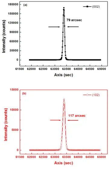
The EQEs are related to internal quantum efficiencies (IQE) and light extraction. It was reported that the output power and IQE can be improved by decreasing the defect density of the substrate, which is attributed to the reduction of nonradiative recombination centers [7]. Therefore, we grew high-quality GaN substrates by the HVPE technique. To assess the overall structural quality of the GaN substrate, x-ray rocking curves were used to measure the crystalline quality of the GaN substrate. Representative rocking curves measured on the (002) and (102) planes are shown in figure1. The resulting full-width at half-maximum (FWHM) measurements are 79 and 117 arcsec for the (002) and (102) planes, respectively.
Figure 2 shows L–I–V characteristics of the fabricated NUV-LEDs. The forward voltages of NUV-LEDs with 2.4 and 3.1 nm QWs grown on GaN substrates are 3.1 and 3.14 V at 20 mA, respectively. With 20 mA injection current, the output powers were 12.7 and 13.2 mW for LEDs with 2.4 and 3.1 nm QWs grown on GaN substrates, respectively. Compared with
Figure 1. FWHM measurement by x-ray diffraction for GaN
substrate at (a) the (002) plane and (b) the (102) plane.
Figure 2. Light output power and forward voltage as a function of
injection current for different thicknesses of QWs.
NUV-LEDs with thinner QWs, 3.9% enhancement of output power can be achieved by widening the QWs. However, wider QWs cannot increase the output power substantially; this may be caused by the considerable amount of downward light in the homoepitaxial LEDs, which is absorbed by the GaN substrate [8]. Therefore, we increased the light extraction by using a back-side etching method in the following step.
Figure 3. A 30◦tile-view and cross-sectional (inset) SEM images
of the surface morphology of N-face GaN substrate at 80◦C in KOH
solutions at various times: (a) before etching and (b) 1 min.
Two approaches can be used to increase the light extraction. One approach is to grow NUV-LED structures on PSS. The other approach is to grow NUV-LED structures on GaN substrate and subsequently immerse these in a KOH solution for 1 min to form the pyramidal N-face GaN structure. Figures 3(a) and (b) are 30◦ tile-view and cross-sectional (inset) SEM images of the surface morphology before and after etching at 80◦C in KOH solutions for 1 min.
A pyramidal structure was observed with the chemical etching solution of N-face GaN. Previously reported chemical etching solutions, such as KOH, sulfuric acid (H2SO4) and PEC
can selectively etch the N-face GaN, but not the Ga-face GaN [9,10]. Because the wet-etching process occurs through the negatively charged OH− ions, Ga-face GaN is more stable than N-face GaN because of the negatively charged triple dangling bonds at the surface of Ga-polar GaN [9,11]. Therefore, the N-face GaN is exposed at the bottom of the GaN substrate. The etching process ended in six {1011} faces of the GaN layer. These results are consistent with those reported by Ng et al [9]. Moreover, the vertical depths of pyramids were in the range of approximately 0.08–0.4 µm. The related details can be found in [12].
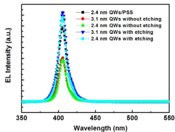
Figure 4 shows RT EL spectra of these fabricated LEDs with 20 mA current injection. All of the EL peak positions of these NUV-LEDs occurred at 405 nm. This can be attributed to the use of the same epitaxial layer with identical
Figure 4. RT EL emission wavelength measured for these LED
samples at a 20 mA current injection.
Figure 5. Light output power and forward voltage as a function of
injection current for different samples.
MQW structure of the NUV-LEDs. The EL intensities of the back-side etching-treated NUV-LEDs and NUV-LEDs on PSSs were larger than those of the NUV-LEDs without etching. This can be attributed to the superior light extraction efficiency for the back-side etching-treated NUV-LEDs and LEDs on PSSs. Moreover, the EL intensities of the back-side etching-treated NUV-LEDs were larger than those of NUV-LEDs on PSSs. The degree of improvement in output power is superior in the case of back-side etching-treated NUV-LEDs.
The output power and the operation voltage as functions of the dc injection current were measured, as shown in figure 5. The forward voltages of back-side etching-treated NUV-LEDs with 2.4 and 3.1 nm QWs grown on GaN substrates are 3.14 and 3.2 V at 20 mA, respectively. The forward voltage of NUV-LEDs with 2.4 nm QWs grown on PSSs is 3.13 V at 20 mA. No substantial difference in I–V curves was observed between these three NUV-LEDs. With 20 mA injection current, the output powers were 25.4 and 27.2 for the back-side etching-treated LEDs with 2.4 and 3.1 nm QWs grown on GaN substrates, respectively, and 23.5 mW for the LEDs with 2.4 nm QWs grown on PSSs. Compared with NUV-LEDs grown on PSSs, the back-side etching-treated NUV-LEDs with various QWs have larger output power than those on PSSs. Such an enhancement can
Phys. Scr. 85 (2012) 045703 Y-H Fang et al
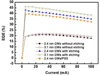
Figure 6. EQEs as a function of injection current for different
samples.
increase the escaping probability of photons emitting from the active layer and reduce the total internal reflection by back-side etching. This indicates that the back-side etching method has a superior capability of enhancing the light extraction. Conversely, one can enhance the 20 mA output power by 100% for 2.4 nm QWs and 106% for 3.1 nm QWs compared with the NUV-LEDs grown on GaN substrates without back-side etching (figure 2) by using the back-side etching method.
Figure6shows the EQEs of NUV-LEDs with and without back-side etching. For the NUV-LEDs of 2.4 and 3.1 nm QWs without etching, wider QWs have larger EQEs because of higher radiative recombination [8]. At an injection current of 20 mA, the corresponding EQEs for 2.4 nm QWs with etching, 3.1 nm QWs with etching and 2.4 nm QWs grown on PSSs were approximately 41, 45 and 38%, respectively. As the forward currents increased to 100 mA, the corresponding EQEs were 35, 38 and 32%. Compared to the 2.4 nm QWs of LEDs grown on PSSs, the EQE enhancement of the 2.4 nm QWs of LEDs with back-side etching was 8 and
8.4% at 20 and 100 mA, respectively. Therefore, back-side etching was a useful method to increase the light extraction efficiency and EQEs.
4. Conclusions
NUV-LEDs were fabricated on PSSs and GaN substrates with and without back-side etching. The output power of NUV-LEDs grown on GaN substrate with back-side etching can be improved by at least 100% at 20 mA compared with that of NUV-LEDs grown on GaN substrates without back-side etching. The corresponding EQEs can be improved by at least 100% at 20 mA. The same trend is observed for the NUV-LEDs grown on PSSs. By using a combination of wider QWs and back-side etching, the highest output power and EQEs can reach approximately 27.2 mW and 45% at 20 mA, respectively. Therefore, the growth of NUV-LEDs on GaN substrates with back-side etching is a promising method for use in NUV-LEDs applications.
References
[1] Mukai T et al 2003 Phys. Status Solidi200 52
[2] Mukai T, Yamada M and Nakamura S 1999 Japan. J. Appl.
Phys.38 3976
[3] Lin C-F, Yang Z-J, Zheng J-H and Dai J-J 2005 IEEE Photon.
Technol. Lett.17 2038
[4] Han D S, Kim J Y, Na S I, Kim S H, Lee K D, Kim B and Park S J 2006 IEEE Photon. Technol. Lett.18 1406
[5] Chang S J et al 2004 IEEE Photon. Technol. Lett.16 1002 [6] Kuo C H et al 2004 Mater. Sci. Eng. B106 69
[7] Akita K, Kyono T, Yoshizumi Y, Kitabayashi H and Katayama K 2007 J. Appl. Phys.101 033104
[8] Cao X A, LeBoeuf S F, D’Evelyn M P, Arthur S D, Kretchmer J, Yan C H and Yang Z H 2004 Appl. Phys. Lett.84 4313 [9] Ng H N, Weimann N G and Chowdhury A 2003 J. Appl. Phys.
94 650
[10] Gao Y, Craven M D, Speck J S, DenBaars S P and Hu E L 2004 Appl. Phys. Lett.84 3322
[11] Li D, Sumiya M, Fuke S, Yang D, Que D, Suzuki Y and Fukuda Y 2001 J. Appl. Phys.90 4219
[12] Fu Y K et al 2011 IEEE Photon. Technol. Lett.23 1373