240 IEEE ELECTRON DEVICE LETTERS, VOL. 27, NO. 4, APRIL 2006
Improved Reliability of HfO
2
/
SiON Gate
Stack by Fluorine Incorporation
Wen-Tai Lu, Chao-Hsin Chiein, Wen-Ting Lan, Tsung-Chieh Lee, Peer Lehnen, and
Tiao-Yuan Huang, Fellow, IEEE
Abstract—Effects of fluorine (F) incorporation on the
relia-bilities of pMOSFETs with HfO2/SiON gate stacks have been
studied. In this letter, fluorine was incorporated during the source/drain implant step and was diffused into the gate stacks during subsequent dopant activation. The authors found that F introduction only negligibly affects the fundamental electrical properties of the transistors, such as threshold voltage Vth, subthreshold swing, gate leakage current, and equivalent oxide thickness. In contrast, reduced generation rates in interface states and charge trapping under constant voltage stress and bias temperature stress were observed for the fluorine-incorporated split. Moreover, the authors demonstrated for the first time that F incorporation could strengthen the immunity against plasma charging damage.
Index Terms—Bias temperature instability (BTI), fluorine (F),
hafnium oxide, plasma charging damage.
I. INTRODUCTION
R
ECENTLY, HfO2 has emerged as the leading high-k dielectric to replace the conventional SiO2. However, a number of pending issues need to be resolved before HfO2 can be inducted into the mainstream ultra-large-scale integra-tion (ULSI) technology. These issues include solving mobility degradation and threshold voltage instability, as well as re-ducing the number of fixed charges and charge traps [1]–[4]. Although there exist numerous literature reports regarding methods to incorporate nitrogen [5], [6] or Si [7], [8] into Hf-based films or stacks so as to improve the film’s quality, however, to the best of our knowledge, the effect of F incorpora-tion on HfO2gate dielectric was seldom addressed [9], [10]. In this letter, fluorine incorporation through fluorine implantation into the source/drain regions was used to evaluate its impact on the constant voltage stress (CVS) instability and negative bias temperature instability (NBTI) of pMOSFETs with HfO2 gate stacks. Our results clearly show that these degradations are improved in the F-incorporated samples. Moreover, because few studies [9] have been performed regarding plasma charging Manuscript received December 2, 2005; revised January 24, 2006. This work was supported in part by the National Science Council, Taiwan, R.O.C., under Contract 94A0500001. The review of this letter was arranged by Editor A. Chatterjee.W.-T. Lu, W.-T. Lan, T.-C. Lee, and T.-Y. Huang are with the Department of Electronics Engineering and Institute of Electronics, National Chiao-Tung University, Hsinchu 300, Taiwan, R.O.C.
C.-H. Chiein is with the Department of Electronics Engineering and Institute of Electronics, National Chiao-Tung University, Hsinchu 300, Taiwan, R.O.C., and also with National Nano Device Laboratories, Hsinchu 300, Taiwan, R.O.C. (e-mail: [email protected]; [email protected]).
P. Lehnen is with Aixtron AG, Aachen 52072, Germany. Digital Object Identifier 10.1109/LED.2006.871539
effects of HfO2 gate stacks, we have therefore carried out a systematic study in this regard and found that larger antenna ratio will result in much severe degradation. More importantly, our data also show that the plasma charging damage can be significantly improved by the F incorporation into the HfO2 gate stacks.
II. EXPERIMENT
pMOSFETs with HfO2/SiON gate stacks were fabricated in this letter. The thin (0.6 nm) interfacial oxynitride layer (SiON) was first grown by rapid thermal processing (RTP) in an N2O ambient at 700◦C. Subsequently, a 3-nm HfO2 layer was de-posited by atomic vapor deposition (AVD) using an AIXTRON Tricent system at a substrate temperature of 500 ◦C. Wafers were then annealed in an N2 ambient at 700 ◦C for 20 s to improve the HfO2film quality. Next, a 200-nm polycrystalline silicon (poly-Si) layer was deposited by low-pressure chemical vapor deposition (LPCVD). Then, the gate electrode was pat-terned through lithographic and etching processes. Some wafers then received a fluorine (F, 2 × 1015 cm−2) ion implantation into the source/drain region without removing the photoresist on the gate electrode. This was deliberately performed to avoid the potential complication caused by fluorine-enhanced boron penetration. After photoresist removal, source/drain regions were formed by regular boron implantation, with the dopants activated at 950 ◦C by rapid thermal annealing for 20 s in an N2 atmosphere. It should be noted that the thermal bud-get of dopant activation also served to diffuse the F species into the HfO2 gate stacks. After passivation layer deposition, contact holes and aluminum metalization were formed. Finally, a forming gas annealing at 400◦C was performed for 30 min to complete the device fabrication.
The equivalent oxide thickness (EOT) of the gate di-electric was extracted from high-frequency (100 kHz) capacitance–voltage (C–V ) curves at strong inversion (EOT = εSiO2/Cinv) without considering the quantum effect.
Charge pumping current was measured with fixed amplitude method at a frequency of 1 MHz [11].
III. RESULTS ANDDISCUSSION
Fig. 1 depicts the typicalId−Vgcurves of pMOSFETs with
HfO2/SiON gate stacks, both with and without F incorporation.
The inset table shows the corresponding transistor parameters. It can be seen that all key device parameters, including the interface state densityNit, EOT,Vth, and gate leakage current, 0741-3106/$20.00 © 2006 IEEE
LU et al.: IMPROVED RELIABILITY OF HfO2/SiON GATE STACK BY FLUORINE INCORPORATION 241
Fig. 1. Typical transfer characteristics of pMOSFETs with HfO2gate stack, both with and without fluorine incorporation.
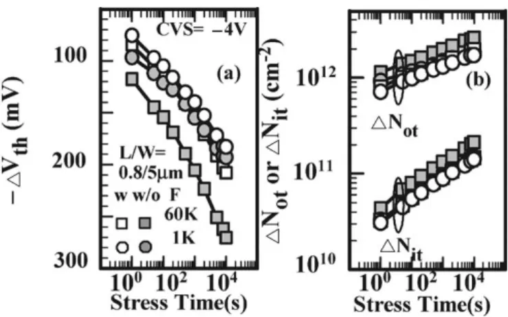
Fig. 2. (a) Threshold voltage shift(∆Vth) and (b) generation of interface states(∆Nit) and trapping charge (∆Not), both plotted in log scale, as
a function of injection charge density(Vg= −4 V). The degradation was
dominated by∆Not, rather than∆Nit.
are essentially indistinguishable between the samples with and without F incorporation. The inset at the upper right corner shows that the distribution of Vth is not affected by the ad-dition of F. All these data suggest that little or no adverse impact on the fundamental electrical properties is achieved with F introduction.
For the reliability evaluation, negative CVS test was per-formed at 25 ◦C, with the transfer curves measured for monitoring ∆Vth at various stressing times. The results are shown in Fig. 2(a). To reduce the unstable fast charge de-trapping effects [1]–[4], a small positive voltage (0.5 V) with a duration of several seconds was applied to detrap these charges before Id−Vg and charge pumping measurements
without inducing extra damage to the gate stacks. This step thus allows much accurate estimation of the slow trap density without the complication due to the interval variation between voltage stressing and parameter measurement. In other words, the precaution allows us to focus on the slow traps in the gate stacks in this letter. It is clear that the F-incorporated sample always shows smaller∆Vth than the control counter-part. To further gain insights into the degradation mechanism
Fig. 3. Threshold voltage shift (∆Vth) as a function of channel length. Devices were stressed at 25◦C andVg= −4 V.
Fig. 4. (a) ∆Vth and (b)∆Nit and ∆Not, for splits with and without F incorporation, as a function of injection charge density atT = 125◦C under stress voltage of−3.5 V.
during voltage stressing, the interface state generation ∆Nit
and the increase of effective bulk trap density∆Notare plotted as a function of the injection charge density in Fig. 2(b). It should be noted that ∆Not was calculated from ∆Vth by assuming that the charge was trapped at the interface between the dielectric and the substrate. Apparently, ∆Not was sig-nificantly larger than ∆Nit, suggesting that the degradation under CVS was dominated by the charge trapping in the bulk of HfO2 films, rather than the generation of interface states, whether fluorine was incorporated or not. Moreover, F incorporation was found being able to suppress the charge trapping in the bulk of HfO2 films. Although reduced charge injection during stressing was a plausible cause for the observed improvement in the F-incorporated split, it contradicted with the observation that the improvement became more visible with decreasing channel length, as show n in Fig. 3. If the improvement seen in F-incorporated split was indeed due to reduced injection charges, no dependence of the improve-ment on the channel length should be expected. Therefore, we concluded that the improvement was indeed the result of the F incorporation.
242 IEEE ELECTRON DEVICE LETTERS, VOL. 27, NO. 4, APRIL 2006
Fig. 5. Time dependence of (a) ∆Vth and (b) ∆Nit under CVS for pMOSFETs with different AARs, both with and without F incorporation. Higher AAR results in much severe degradation, whereas the F-incorporated split exhibits lower∆Vthand∆Nit.
Fig. 4(a) and (b) compares the dependence of threshold volt-age shift and the interface generation, respectively, on injection charge density for splits with and without F incorporation. The BT stress condition was Vg= −3.5 V under 125 ◦C. It can
be seen that F-incorporated films exhibit NBTI improvement similar to fluorine-induced NBTI improvement in SiOF case [12], [13]. The major degradation of NBTI is caused by the positive charge trapping in the films rather than the interface generation, suggesting that the positive charge trapping is not entirely caused by the H+ capturing. Therefore, in addition to positive charge caused by H species, a significant amount of extra trapping centers must be present in the HfO2/SiON
gate stack. Fluorine atoms seem to effectively decorate these trapping centers, leading to reduced degradation.
In our process, the photoresist layer that remained after metal patterning was stripped with O2plasma in a downstream plasma asher, whose configuration and plasma potential distri-bution could be found in [14]. Using CHARM-2 wafer sensor, it has been previously shown [14] that the potential distribution was highly negative and positive at the wafer center and edge, respectively. Fig. 5 shows the time evolution of the threshold voltage shift and interface state generation for the devices with area antenna ratios (AARs) of either1 × 103or6 × 104, both with and without F incorporation. All measurements were performed on devices located at the same die location (i.e., wafer center). Fig. 4 shows that the hole trapping in the bulk, rather than the interface generation, is the preponderant mecha-nism responsible for the degradation. From the Weibull plot of Vthfor the fresh devices located at the wafer center, it is found that the control devices with AAR of6 × 104depict larger|Vth| values than their counterparts with F incorporation (data not shown). This is consistent with previous results in CVS and NBTI. Moreover, all these results are in-line with the hypothesis that plasma antenna charging effect creates more hole traps in the HfO2/SiON gate stacks and that F-incorporated devices are more robust to plasma charging effect.
IV. CONCLUSION
In this letter, we found that the reliabilities of pMOSFETs with HfO2/SiON gate stacks under both CVS and NBTI stresses are significantly improved by the F incorporation. In addition, we demonstrated for the first time that plasma charging effect induces hole trapping in the HfO2/SiON gate stacks. Finally, we found that the plasma charging effect can be effectively suppressed with F incorporation.
REFERENCES
[1] S. Zafar, A. Callegari, E. Gusev, and M. Fischetti, “Charge trapping related threshold voltage instabilities in high permittivity gate dielectric stacks,” J. Appl. Phys., vol. 93, no. 11, pp. 9298–9303, Jun. 2003. [2] J. Zhu, T. P. Ma, S. Zafar, and T. Tamagawa, “Charge trapping in ultrathin
hafnium oxide,” IEEE Electron Device Lett., vol. 23, no. 10, pp. 597–599, Oct. 2002.
[3] E. P. Gusev and C. P. D’Emic, “Charge detrapping in HfO2high-k gate stacks,” Appl. Phys. Lett., vol. 83, no. 25, pp. 5223–5225, Dec. 2003. [4] A. Kerber, E. Carter, L. Pantisano, M. Rosmeulen, R. Degraeve,
T. Kauerauf, G. Groeseneken, H. E. Maes, and U. Schwalke, “Charac-terization ofVTinstability in SiO2/HfO2gate dielectrics,” in Proc. 41st
Int. Reliab. Phys. Symp., Dallas, TX, 2003, p. 41.
[5] C. S. Kang, H. Cho, R. Choi, Y. Kim, C. Y. Kang, S. J. Rhee, C. Choi, M. S. Akbar, and J. C. Lee, “The electrical and material characterization of hafnium oxynitride gate dielectrics with TaN-gate electrode,” IEEE Trans.
Electron Devices, vol. 51, no. 2, pp. 220–227, Feb. 2004.
[6] C. S. Kang, H. Cho, K. Onishi, R. Choi, Y. H. Kim, R. Nieh, J. Han, S. Krishnan, A. Shahriar, and J. C. Lee, “Nitrogen concentration effects and performance improvement of MOSFETs using thermally stable HfOxNygate dielectrics,” in IEDM Tech. Dig., 2002, pp. 865–868. [7] T. Iwamoto, T. Ogura, M. Terai, H. Watanabe, N. Ikarashi, M. Miyamura, T. Tatsumi, M. Saitoh, A. Morioka, K. Watanabe, Y. Saito, Y. Yabe, T. Ikarashi, K. Masuzaki, Y. Mochizuki, and T. Mogami, “A highly manu-facturable low power and high speed HfSiO CMOS FET with dual poly-Si gate electrodes,” in IEDM Tech. Dig., 2003, pp. 639–642.
[8] Y. Kim, H. J. Lim, H. Jung, J. Lee, J. Park, S. K. Han, J. H. Lee, S. Doh, J. P. Kim, N. I. Lee, Y. Chung, H. Y. Kim, N. K. Lee, S. Ramanathan, T. Seidel, M. Boleslawski, G. Irvine, B. Kim, H. Lee, and H. Kang, “Char-acteristics of ALD HfSiOxusing new Si precursors for gate dielectric applications,” in IEDM Tech. Dig., 2004, pp. 511–514.
[9] H.-H. Tseng, M. E. Ramon, L. Hebert, P. J. Tobin, D. Triyoso, S. Kalpat, J. M. Grant, Z. X. Jiang, D. C. Gilmer, D. Menke, W. J. Taylor, O. Adetutu, and B. E. White, “Threshold voltage instability and plasma induced damage of poly-Si/HfO2devices -positive impact of deuterium incorporation,” in Proc. ICICDT, 2004, pp. 255–259.
[10] A. Mineji, Y. Tamura, T. Watanable, H. Ozaki, F. Ootsuka, T. Aoyama, K. Shibata, K. Tsujita, N. Ohashi, M. Yasuhira, and T. Arikado, “Integration of manufacturable 65 nm-node HfSiON transistors optimized with low-thermal-budget CMOS process,” in IEDM Tech. Dig., 2004, pp. 927-930.
[11] A. Kerber, E. Carter, L. Pantisano, M. Rosmeulen, R. Degraeve, G. Groeseneken, H. E. Maes, and U. Schwalke, “Charge trapping in SiO2/HfO2gate dielectrics: Comparison between charge pumping and pulsedID−VG,” Microelectron. Eng., vol. 72, no. 1–4, pp. 267–272, Apr. 2004.
[12] C. H. Liu, M. T. Lee, C. Lin, J. Chen, K. Schruefer, J. Brighten, N. Rovedo, T. B. Hook, M. V. Khare, S. Huang, C. Wann, T. Chen, and T. H. Ning, “Mechanism and process dependence of negative bias temperature instability (NBTI) for pMOSFETs with ultrathin gate di-electrics,” in IEDM Tech. Dig., 2001, pp. 861–864.
[13] Y. Mitani, M. Nagamine, H. Satake, and A. Toriumi, “NBTI mechanism in ultra-thin gate dielectric-nitrogen-originated mechanism in SiON,” in
IEDM Tech. Dig., 2002, pp. 509–512.
[14] C. C. Chen, H. C. Lin, C. Y. Chang, M. S. Liang, C. H. Chien, S. K. Hsien, and T. Y. Huang, “Improved immunity to plasma damage in ultra thin nitrided oxides,” IEEE Electron Device Lett., vol. 21, no. 1, pp. 15-17, Jan. 2000.