Effect of Top Electrode Material on Resistive
Switching Characteristics in MnO2 Nonvolatile Memory Devices
Yu-Ting Tsai a, Ting-Chang Chang b,*, Chao-Cheng Lin c, Lan-Shin Chiang a, Shih-Cheng Chenc, Simon M. Sze a and Tseung-Yuen Tseng a
a. Department of Electronics Engineering & Institute of Electronics, National Chiao
Tung University, Hsin-Chu 300, Taiwan, R.O.C.
b. Department of Physics and Institute of Electro-Optical Engineering, & Center for
Nanoscience and Nanotechnology, National Sun Yat-Sen University, Kaohsiung, 804, Taiwan, R.O.C.
c. Green Energy & Environment Research Labs. , Industrial Technology Research
Institute, Hsinchu 310, Taiwan, R.O.C.
d. Department of Electrical Engineering & Institute of Electronic Engineering, National
Tsing Hua University, Taiwan
The influence of top electrode material on the resistive switching properties of MnO2-based memory film using Pt as a bottom
electrode was investigated in this study. In comparison with Pt/ MnO2/Pt and Al/ MnO2/Pt devices, the Ti/ MnO2/Pt device
exhibits resistive switching current–voltage (I–V ) curve, which can be traced and reproduced more than 105 times only showing a little decrease of resistance ratio between high and low resistance states. Furthermore, transmission electron microscopy analyses are used to confirm the crystalline structure of MnO2 on Pt bottom
electrode. Secondary ion mass spectrometry reveals a change of oxygen distribution in MnO2 thin film due to material
characteristic of variant top electrodes. We suggest that the interface between MnO2 and electrodes play an important role on
the resistive switching behaviors.
Introduction
The next-generation nonvolatile memory (NVM) has attracted extensive attention due to the conventional memories approaching their scaling limits. The electric-field controlled resistive random access memory (RRAM) by using metal oxide has been projected in the form of metal/oxide/metal structures and attracted considerable attention because of its simple structure, long retention time, small size, fast switching speed, low temperature process and compatibility with complementary-metal-oxide-semiconductor (CMOS) process.(1), (2) Resistive switching phenomena have been observed in various oxide materials which are doped perovskite SrZrO3,(3) ferromagnetic materials such as (Pr, Ca)
MnO3,(4) and binary transition metal oxides such as NiO,(2),(5) TiO2,(6) CuxO,(7),(8)
and Al2O3.(9), (10) However, to date, there has been relatively little research conducted
materials analyses. Although the influence of top electrode on the resistive switching properties has been investigated, the mechanism is still unknown.
In this paper, the secondary ion mass spectrometry (SIMS) was presented to analyze the depth profile of TE/MnO2/Pt structure with different top electrodes. It was found that
the oxygen distribution at the interface can influence the electric properties of the structure. By using this material analysis, the switching mechanism can be further clarified.
Experimental Details
The process flow and memory structure is shown in figure 1. The memory devices were used to be fabricated on the boron-doped p-type (100) silicon wafer. After the standard Radio Company of America (RCA) cleaning, a 300-nm-thick SiO2 films as the buffer
oxide was thermally grown by a horizontal furnace, which was followed by a 20-nm-thick Ti layer and then an 80-nm-20-nm-thick Pt layer deposited by a DC magnetron reactive sputtering. Subsequently, a 40 nm MnO2 films were deposited on Pt/Ti/SiO2/Si substrate
by electron beam evaporation at room temperature. Finally, various top electrodes (TE), Pt, Al, and Ti, were deposited on the MnO2 films by using electron beam evaporation or
DC magnetron sputtering to form a TE/MnO2/Pt (metal/resistor/metal, MRM) sandwich
structure. All processes were completed at room temperature; therefore it can be also applied on glass or flexible substrate.
The area of the TE defined by a shadow mask was 3.1 × 10⁻⁴ cm2. Transmission electron microscopy (TEM) are use to analyze the microstructure of MnO2 thin films.
The concentration distribution of oxygen was examined by Secondary ion mass spectrometry (SIMS). Electrical properties were measured using the Agilent B1500 semiconductor characterization system at room temperature. The DC sweeping voltage was applied to the top electrode and the bottom electrode was grounded. Compliance current was used to set a limit to the current flow in order to avoid a complete dielectric breakdown.
Results And Discussion
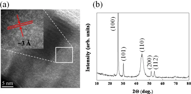
Figure 2 (a) shows the cross-section TEM image of Al/MnO2/Pt films structure.
Columnar microstructures were observed from bottom to top in the MnO2 layer. The
width of the columnar grains is about 9~10 nm, the atoms arrange periodically and the lattice constant is about 3 Å as shown in the inset of Fig. 2 (a). To investigate the crystalline structure of the columnar grains, the XRD spectra of MnO2 on the bottom Pt
electrode can be found in Fig. 2 (b). It can be readily indexed to phase of ε-MnO2 with
lattice constants a = 2.80 Å and c = 4.45 Å, (11) moreover, it can be found that MnO2
films have a polycrystalline hexagonal phase structure.
Figure 2. (a) The cross-section TEM images and (b) XRD spectra of the MnO2 thin film.
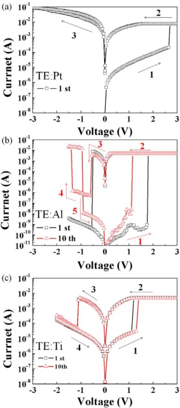
Figure 3 depicts the current–voltage (I–V) curves of the MnO2 RRAM device. When
a sweep positive voltage was applied, the current of the device increased rapidly, and the device was switched from high resistance state (HRS) to low resistance state (LRS), defined as the “set” process. On the other hand, when a sweep negative voltage was applied, the current decreased rapidly and the device was switched from LRS to HRS, defined as the “reset” process. A current compliance was set at 8 mA during the set process to prevent permanent breakdown of the device. There has been reported that an electroforming process is necessary for the initialization of the resistive memory switching.(6), (12) Because the forming voltage is much larger than operation voltage, the large power of forming process may damage parts of the devices. This will result in a lower yield of the devices. However, our devices processed resistive switching characteristic without forming process. It can be attributed to the grain boundaries which can provide faster transport paths for oxygen ions in the MnO2 layer.
Figure 3. I-V curves of switching memory cell in semilog scale of (a) Pt/MnO2/Pt (b)
be seen that after operating several times, the LRS current became unstable to reach HRS (the 10th switching time in the Fig.) and most of the devices broke down after a few set/reset cycles. From Fig. 3 (c), it could be noticed that I-V curves with successive memory switching were greatly stabilized by Ti top electrode and the ratio of resistance between HRS and LRS was larger enough for distinguish 0 or 1.
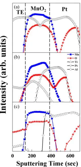
When the device switched from HRS to LRS, the oxygen vacancies were created in the MnO2 film due to oxygen ions drifted to TE by electric field. The MnO2 thin film
became metal-like MnOx (x<2) at LRS. On the order hand, when MnOx switched from
LRS to HRS, it needed oxygen ions to recover MnOx for achieving HRS.(13) Fig. 4 (a),
(b) and (c) is the comparison of SIMS depth profile for various top electrodes, Pt, Al, and Ti, respectively deposited on MnO2/Pt device. As shown in Fig. 4 (a), it could be found
that the oxygen concentration at the interface of Pt/MnO2 was very low because oxygen
can easily diffuse into atmosphere along the Pt grain boundaries. (14)When Pt/MnO2/Pt
device switches from HRS to LRS at the first time, the oxygen ions drift through the Pt electrode by electric field and conducting paths were formed. However Pt cannot act as a source and reservoir for oxygen ions, the oxygen vacancies cannot be recovered. Therefore, the device cannot switch from LRS to HRS.
In the Fig. 4 (b), oxygen concentration could be found at the interface of Al and MnO2. The result can be attributed to a dense AlOx thin film formed at the interface after
several operation times. However, the oxygen concentration at the interface of Al/MnO2
was low. During operation, the oxygen ions are not enough for oxygen vacancies to be recovered, and therefore it makes the electrical property to become unstable [Fig. 3 (b)].
Fig. 4 (c) illustrates that the concentration of oxygen at the Ti/MnO2 interface is
abundant because Ti can serve as a reservoir for oxygen ions storing. Moreover, Ti can steadily provide enough oxygen ions to recover oxygen vacancies of MnOx during reset
operation. Therefore, the switching characteristic of Ti/MnO2/Pt device is better than
Al/MnO2/Pt device.
Fig. 5 shows the endurance and retention characteristics of HRS and LRS in the Ti/MnO2/Pt device. The pulse programming/erase voltages were +2.5 and -2.6 V and the
pulse width was 100ns and 300ns, respectively. Fig. 5(a) shows the resistance ratio of HRS and LRS of this device was about 100 times, and the on-off resistance state was gradually stabilized over 105 times of cycles. Fig. 5(b) shows the retention behavior at 0.2V reading voltage of the memory in Ti/MnO2/Pt device at 85℃. The resistance ratio
between LRS and HRS is stable for 104 seconds retention time. These results indicate that the Ti/MnO2/Pt device is a great candidate for non-volatile memory application.
Figure 4. Secondary ion mass spectra (SIMS) of (a) Pt/MnO2/Pt (b) Al/MnO2/Pt (c)
Conclusions
In conclusion, we have deposited resistive switching layer of MnO2 with columnar
microstructures at room temperature. The Ti/MnO2/Pt device can be operated at low
voltage without forming process. In addition, Ti/MnO2/Pt device exhibited better resistive
switching properties which could be traced and reproduced over than 105 times between LRS and HRS in comparison with Pt/MnO2/Pt and Al/MnO2/Pt devices. The different
oxygen ions distribution at the interface of TE and MnO2 shows a large dependence with
the different resistive switching properties. The results suggest the interface between MnO2 and the top electrode plays an important role in the memory switching.
Acknowledgments
This work was performed at National Nano Device Laboratory and was supported by the National Science Council of the Republic of China under Contract Nos. NSC99-2120-M-110-001, NSC99-2221-E-009-165-MY2 and NSC-97-2112-M-110-009-MY3.
References
1. R. Waser and M. Aono, Nature Mater. 6, 833 (2007).
2. Y. Sato, K. Tsunoda, K. Kinoshita, H. Noshiro, M. Aoki, and Y. Sugiyama, IEEE Trans. Electron Devices 55, 1185 (2008).
3. C. Y. Liu, P. H. Wu, A. Wang, W. Y. Jang, J. C. Young, K. Y. Chiu, and T.-Y. Tseng, IEEE Electron Device Lett. 26, 351 (2005).
4. J. Rodrıguez Contreras, H. Kohlstedt, U. Poppe, R. Waser, C. Buchal, and N. A. Pertsev, Appl. Phys. Lett. 83, 4595 (2003).
5. D. C. Kim, M. J. Lee, S. E. Ahn, S. Seo, J. C. Park, I. K. Yoo, I. G. Baek, H. J. Kim, E. K. Yim, J. E. Lee, S. O. Park, H. S. Kim, U-In Chung, J. T.Moon, and B. I. Ryu, Appl. Phys. Lett. 88, 232106 (2006).
6. Y.H. Do, J.S. Kwak, J.P. Hong, K.H. Jung, H.S. Kim, J. Appl. Phys. 104 114512 (2008).
7. A. Chen, S. Haddad, Y.-C. Wu, T.-N. Fang, Z. Lan, S. Avanzino, S. Pangrle, M. Rathor, W. Cai, N. Tripsas, C. Bill, M. VanBuskirk, M. Taguchi, Int. Electron Devices Meet., Tech. Dig. 746 (2005).
8. T.-N. Fang, S. Kaza, S. Haddad, A. Chen, Y.-C. Wu, Z. Lan, S. Avanzino, D. Liao, C. Gopalan, S. Choi, S. Mahdavi, M. Buynoski, Y. Lin, C. Marrian, C. Bill, M. VanBuskirk, M. Taguchi, Int. Electron Devices Meet., Tech. Dig. 789 (2006). 9. S. Kim and Y. K. Choi, Appl. Phys. Lett. 92, 223508 (2008).
10. Y. T. Tsai, T. C. Chang, C. C. Lin, S. C. Chen, C. W. Chen, S. M. Sze, F. S. Yeh and T. Y. Tseng, Electrochem. Solid-State Lett., Volume 14, Issue 3, pp. H135-H138 (2011).
11. Visser, J., Technisch Physische Dienst, Delft, The Netherlands, ICDD Grant-in-Aid, (1979)
12. C.-Y. Lin, C.-Y. Wu, C.-Y. Wu, C. Hu, and T.-Y. Tseng, J. Electrochem. Soc., 154, G189 (2007).
13. B.Gao, S. Yu, N.Xu, L.F. Liu, B. Sun, X.Y. Liu, R.Q. Han, J.F. Kang, B.Yu, Y.Y. Wang, Int. Electron Devices Meet., Tech. Dig. 563 (2008).
14. R. Schmiedl, V. Demuth, P. Lahnor, H. Godehardt, Y. Bodschwinna, C. Harder, L. Hammer, H.-P. Strunk, M. Schulz, and K. Heinz, Appl. Phys. A: Mater. Sci. Process. 62, 223 (1996).