Recombination zone in mixed-host organic light-emitting devices
Chih-Hung Hsiao, Yan-Hau Chen, Tien-Chun Lin, Chia-Chiang Hsiao, and Jiun-Haw Leea兲 Graduate Institute of Electro-Optical Engineering, National Taiwan University, No. 1, Sec. 4,
Roosevelt Road, Taipei, Taiwan 106, Republic of China and Department of Electrical Engineering, National Taiwan University, No. 1, Sec. 4, Roosevelt Road, Taipei, Taiwan 106, Republic of China 共Received 13 May 2006; accepted 31 August 2006; published online 19 October 2006兲
In this letter, the authors had quantitatively investigated the recombination zone in the mixed-host 共MH兲 emitting layer 共EML兲 of an organic light-emitting device with different mixed ratios experimentally and theoretically. The MH-EML consisted of a hole-transport layer 共HTL兲 and an electron-transport layer fabricated by coevaporation. When the mixed ratio of the HTL in the EML increases, the driving voltage increases then decreases; this can be well demonstrated by an electrical model with different carrier mobilities. A blueshift was also observed due to the solid state solvation effect combined with the exciton shift from the anode to the cathode side. © 2006
American Institute of Physics. 关DOI:10.1063/1.2361266兴
In 1987, Tang and Vanslyke demonstrated organic light-emitting devices 共OLEDs兲, consisting of several layers of amorphous organic films with the thicknesses of tens of na-nometers, with a driving voltage of less than 10 V.1 From then on, OLEDs have attracted much attention because of their advantages such as low-power consumption, high brightness, high contrast, and potentially low cost.2 How-ever, their operation lifetime is still one of the major limita-tions for OLED applicalimita-tions as compared to other competi-tive display technologies such as semiconductor light-emitting diodes and liquid crystal displays.3
In order to elongate the operation lifetime, a mixed-host 共MH兲 structure had been introduced as the host of the emit-ting layer 共EML兲.4,5 In a conventional heterojunction 共HJ兲 OLED, the interface of the hole-transporting layer 共HTL兲 and EML builds up a barrier to enhance carrier confinement, which improves the device efficiency.1 However, the accu-mulated holes in the EML near the interface formed chemi-cally unstable cations, which accelerated the formation of nonradiative trapping centers, thus resulting in luminance de-cay and voltage increase of an OLED.6By coevaporating the HTL and the electron-transport layer共ETL兲 material as the host of the EML, the HTL/EML interface became blurry. This reduced carrier accumulation can broaden the emission zone, elongating the operation lifetime. This blurring bound-ary raises the probability of penetration of holes into EML so that excitons are generated over wider region in EML instead of narrower region around the interface of HTL/EML. In this regard, the broadening of emission zone, which indicates that the leakage of the carriers to the electrodes is dominant, de-creases device efficiency.7Typically, the operation lifetime of MH-OLEDs can be extended by a factor of 6 as compared to the conventional HJ ones.8,9
However, in the absence of the carrier confinement of the conventional HJ structure, the MH-OLED exhibits a higher carrier leakage and lower current efficiency. Further-more, the bipolar characteristic of the EML would shift the recombination zone from the interface into the EML, causing a reduction in current efficiency due to the quenching by the metal electrodes. To optimize the device characteristics of a MH-OLED, different layer thicknesses and mixed ratios
were tested and results were discussed qualitatively.10In our experiment we had developed an electrical and an optical model from basic equations to quantitatively simulate the current density-voltage 共J-V兲 curves and electrolumines-cence共EL兲 spectra of the MH-OLEDs with different mixed ratios. Electron and hole mobilities of the MH layers with different mixture concentrations were extracted, which can well explain the J-V characteristics of MH-OLEDs. Based on the mobility values, carrier and exciton distributions can be used to calculate the EL spectral shift.
Our fabrication and measurement details are shown in Ref. 11.11 Here, we used N , N
⬘
-diphenyl-N , -diphenyl-N
⬘
-bis共1-napthyl兲-1,1⬘
-biphenyl-4,4⬘
-diamine 共NPB兲 as the HTL material and tris-共8-hydroxyquinoline兲 aluminum 共Alq3兲 as the ETL material. The EML was a mixture of NPB and Alq3 with different mixed ratios. LiF and aluminum 共Al兲 were served as the electron-injection layer and the cathode. Our device structures were ITO/ NPB共20 nm兲/ NPB: Alq3共80 nm兲/Alq3共20 nm兲/LiF共1.2 nm兲/Al共150 nm兲. Devices A, B, C, D, and E corresponded to the NPB: Alq3 mixed ratios of 0:1, 1:3, 1:1, 3:1, and 1:0, respectively. In our simulations, we developed a numerical method for investi-gating the electrical properties of an OLED based on the drift-diffusion equations containing charge carrier drift with field-dependent mobility, thermionic emission, HJ interface, and recombination process.12,13 The input data of such an electrical simulation included the carrier mobility and band diagram of the organic materials, and the layer thicknesses of an OLED. From this electrical simulation model, we achieved the J-V characteristics and the distribution of the electric field, carrier and exciton concentrations, and recom-bination rate in an OLED. The exciton distribution was used as the input of the optical simulation program based on gen-eral electromagnetic theory.14 In addition to the exciton dis-tribution, the other input parameters comprised the layer thickness, the real and imaginary parts of refractive index of each layer, and the photoluminescence 共PL兲 of the emitter. The outputs of this program encompassed the spectrum, in-tensity, and viewing angle of an OLED.Figure 1共a兲 shows the experimental and simulated J-V characteristics. The solid lines and the dots show the simu-lation and experiment results, respectively. The values of the highest occupied molecule orbital 共HOMO兲 and the lowest
a兲Electronic mail: [email protected]
APPLIED PHYSICS LETTERS 89, 163511共2006兲
0003-6951/2006/89共16兲/163511/3/$23.00 89, 163511-1 © 2006 American Institute of Physics Downloaded 06 Feb 2009 to 140.112.113.225. Redistribution subject to AIP license or copyright; see http://apl.aip.org/apl/copyright.jsp
unoccupied molecule orbital 共LUMO兲 of NPB 共Alq3兲 are 5.4 eV共3.0 eV兲 and 2.4 eV 共5.7 eV兲. The work functions of indium tin oxide共ITO兲 and LiF:Al are 4.9 and 3.2 eV.15 In our simulation, the only fitting parameter was electric-field 共F兲 dependent carrier mobilityof the MH layers, following the Poole-Frenkel form:16
=0exp
冉
冑
F E0
冊
, 共1兲
where0 is the zero-field mobility and E0 is a constant. In our fitting, the o and Eo values of NPB for holes were
po= 1.8⫻10−4cm2/ V s and Epo= 2⫻105V / cm, and for electrons were no= 1⫻10−10cm2/ V s and Eno= 1 ⫻108V / cm. The
o and Eo values of Alq3 for holes were
po= 6⫻10−11cm2/ V s and Epo= 1.25⫻104V / cm, and for electrons were no= 4.6⫻10−9cm2/ V s and Eno= 1.4 ⫻104V / cm, respectively.17,18
In terms of the mobilities in MH layer, theovalues were varied to fit the experimental results on condition of the constant Eo values. As shown in Fig. 1共b兲, the fitted hole 共electron兲 mobility increases 共de-creases兲 almost linearly with increasing 共decreasing兲 HTL material composition in mixed ratio.
The holes and electrons mainly hop through the NPB and Alq3molecules, respectively. In light of the energetically favorite, the hole and electron mobilities in MH layers were lower than the values in the pure NPB and Alq3. On the other hand, as shown in Fig.1共a兲, the driving voltage increases and then decreases with increasing HTL material concentration. In the case of conventional HJ device, the thicker NPB ex-hibited lower driving voltage with the constant total organic thickness since the hole mobility of NPB was two orders of magnitude higher than the electron mobility of Alq3.15 In MH devices, the monotonically decreasing driving voltage did not occur as expected in HJ devices. The discrepancy is the bipolar carrier transport property in MH device. Raising
NPB concentration in MH layer led to the enhanced hole current and reduced electron current. The hole-current en-hancement did not compensate the electron-current decline when the HTL ratio increased from 0% to 25%共from devices A to B兲. This unbalanced change in opposite carrier currents explains the voltage increasing in device B as compared with device A. The sequential increase of HTL material concen-tration from 25% to 100% resulted in the voltage reduction from devices C to E on account of rapidly boost of hole current.
Figure2 shows the simulation results of the recombina-tion rate distriburecombina-tion in the MH-OLEDs. With increased NPB ratio in MH layer, the recombination zone shifted from the HTL/EML interface共device A兲, broadenened 共devices B, C, and D兲, and finally shrank to the interface of EML/ETL 共de-vice E兲. Since the energetic offset of the LUMO between NPB and Alq3 was larger than that of HOMO, the penetra-tion of holes into the Alq3 layer共devices C, D, and E兲 was easier than that of electrons into the NPB共devices A and B兲. The wide recombination zone of the MH-OLED is well known to interpret its longer lifetime as compared with that of the HJ-OLEDs.7
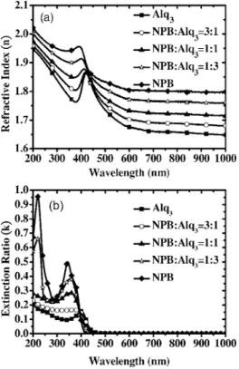
We have quantitatively demonstrated the recombination zone distribution and the mobility change with different mixed ratios. Once the recombination distribution was ob-tained, we used it to derive the exciton distribution, an input of our optical simulation model as described in Ref. 19.19 The other input parameters included refractive index共n兲 and extinction coefficient共k兲 values of each layer, and PL spectra of the EML.20 Figure 3 shows the n-k values at different wavelengths for the MH thin films. We can see that the re-fractive index of pure NPB was the highest. As the Alq3ratio in MH layer increased, the refractive index values decreased monotonically. The extinction coefficients of NPB, Alq3, and the MH-EML were negligibly nearly zero within the emis-sion spectrum共i.e., 450–700 nm兲. Furthermore, the n-k val-ues of the MH layers were close to the linear interpolations of pure NPB and Alq3. This means that MH layers were physically mixed without chemical interaction from mesos-copic viewpoint.
It was a typical solid state solvation effect 共SSSE兲 that the PL peak exhibited a blueshift from 526, 525, 521 to 517 nm when the NPB ratio changed from 0%, 25%, 50% to 75%.21 Figure 4 shows the measured EL spectra of all devices. The measured and simulated spectral peaks blue-shifted from 555, 543, 537, 529 to 522 nm and 557, 546, 537, 535 to 531 nm, for devices A, B, C, D, and E,
respec-FIG. 1.共a兲 Experimental 共dots兲 and stimulated 共solid lines兲 J-V character-istics of the five devices.共b兲 Fitted zero-field carrier mobilities of EML with different mixed ratios.
FIG. 2. Recombination distribution in MH-OLEDs. 20 and 100 nm indicate the interface of NPB/MH and MH/ Alq3, respectively.
163511-2 Hsiao et al. Appl. Phys. Lett. 89, 163511共2006兲
tively. The experimental results matched well with that from the simulation program. Note that there was no adjustable input parameter in this simulation. The peak shift of the EL was much more than that of the PL, indicating the blueshift with increased NPB ratio came not only from the SSSE but also from the optical interference effect. Typically, in the studied range, the EL spectrum reveals a blueshift when the exciton distribution shifts from the anode to the cathode side,13 as is shown in Fig.2.
In conclusion, the recombination distributions in the MH-EML with different mixed ratios were studied. We found that the recombination zone that initially resided at the HTL/EML interface extended into the MH layer and piled up at the EML/ETL interface as the increasing HTL material ratio in MH layer. A quantitatively electrical model, based on the mobility change with different mixing ratios, was estab-lished. Good agreement between experimental and simulated EL spectra suggests that the EL spectral shift came not only from the intrinsic PL spectral shift but also from the extrinsic optical interference effect that originated from the distribu-tion of radiative dipoles, namely, exciton distribudistribu-tion.
This work was supported by the National Science Coun-cil, R.O.C., under Grant No. NSC 95-2221-E-002-305 and by Aixtron Corporation.
1C. W. Tang and S. A. VanSlyke, Appl. Phys. Lett. 51, 913共1987兲. 2C. W. Tang and S. A. VanSlyke, J. Appl. Phys. 65, 3610共1989兲. 3J. H. Lee, J. J. Huang, C. C. Liao, P. J. Hu, and Y. Chang, Chem. Phys.
Lett. 402, 335共2005兲.
4H. Aziz, Z. D. Popovic, N.-X. Hu, A.-M. Hor, and G. Xu, Science 283, 1900共1999兲.
5A. B. Chwang, R. C. Kwong, and J. J. Brown, Appl. Phys. Lett. 80, 725 共2002兲.
6D. Y. Kondakov, J. R. Sandifer, C. W. Tang, and R. H. Young, J. Appl. Phys. 93, 1108共2003兲.
7V. E. Choong, S. Shi, J. Curless, C. L. Shieh, H. C. Lee, J. Shen, and J. Yang, Appl. Phys. Lett. 75, 172共1999兲.
8J. Kalinowski, L. C. Palilis, W. H. Kim, and Z. H. Kafafi, J. Appl. Phys.
94, 7764共2003兲.
9S. W. Liu, C. A. Huang, J. H. Lee, K. H. Yang, C. C. Chen, and Y. Chang, Thin Solid Films 453–454, 312共2004兲.
10J. H. Lee, C. I. Wu, S. W. Liu, C. A. Huang, and Y. Chang, Appl. Phys. Lett. 86, 103506共2005兲.
11J. H. Lee, M. H. Wu, C. C. Chao, H. L. Chen, and M. K. Leung, Chem. Phys. Lett. 416, 234共2005兲.
12P. S. Davids, I. H. Campbell, and D. L. Smith, J. Appl. Phys. 82, 6319 共1997兲.
13E. Tutis, M. N. Bussac, B. Masenelli, M. Carrard, and L. Zuppiroli, J. Appl. Phys. 89, 430共2001兲.
14H. C. Chen, J. H. Lee, C. C. Shiau, C. C. Yang, and Y. W. Kiang, J. Lightwave Technol. 24, 2450共2006兲.
15S. J. Martin, G. L. B. Verschoor, M. A. Webster, and A. B. Walker, Org. Electron. 3, 129共2002兲.
16W. Brütting, S. Berleb, and A. G. Mückl, Org. Electron. 2, 1共2001兲. 17B. J. Chen, W. Y. Lai, Z. Q. Guo, C. S. Lee, S. T. Lee, and W. A.
Gambling, Appl. Phys. Lett. 75, 4010共1999兲.
18B. Chen, C. S. Lee, S. T. Lee, P. Webb, Y. C. Chan, W. Gambling, H. Tian, and W. Zhu, J. Appl. Phys. 39, 1190共2000兲.
19B. W. D. Andrade, M. E. Thompson, and S. R. Forrest, Adv. Mater. 共Wein-heim, Ger.兲 14, 147 共2002兲.
20J. H. Lee, C. C. Liao, P. J. Hu, and Y. Chang, Synth. Met. 144, 279 共2004兲.
21V. Bulović, R. Deshpande, M. E. Thompson, and S. R. Forrest, Chem. Phys. Lett. 308, 317共1999兲.
FIG. 3. 共a兲 Refractive index and 共b兲 extinction coefficient spectra of the MH-EMLs.
FIG. 4. Measured EL spectra of the five devices.
163511-3 Hsiao et al. Appl. Phys. Lett. 89, 163511共2006兲