A 2V Clock Synchronizer using Digital Delay-Locked Loop
Chomg-Sii Hwang, Wang-Chih Chung, Chih-Yong Wang, Hen-Wai Tsao, Shen-Iuan Liu
National Taiwan University Department of Electrical Engineering, Taipei, Taiwan 1061 7, R.O.C. Email : [email protected]
Abstract : A 2V clock synchronizer chip using digital delay-locked loop is presented. It is targeted to provide synchronous clock distribution in high-speed digital systems. A simple structure with a counter-based delay line is used for compensating the skew caused by process, voltage, temperature and length. A stability criterion is also obtained. Experimental results have demonstrated its advantages like good stability, wide tuning range and low power consumption.
I. INTRODUCTION
Due to the rapid progress in modem technology, the speed of synchronous data transfer among boards may be up to lOOMHz[l]. Clock skew becomes an important issue for both larger die size and higher system clock frequency. Clock skew among chips at different locations may degrade the system performance, and even cause system malfimction. The major reason for clock skew comes from the system clock distribution and the propagation delay of the clock chip. The clock skew resulting from propagation delay is dependent on process, voltage, temperature, and length (PVTL), which are not easy to be eliminated. Traditional methods like analog phase-locked loop (PLL)/delay-locked loop (DLL) suffer from larger power or shorter deskewing range[3-41. Altematively, digital DLL’s [l-21 will provide good immunity to power supply noise and PVTL effects. Comparing to analog method, digital DLL can provide larger deskewing range and consume lower power in standby mode. Especially, digital DLL’s will provide good ability of technology migration in scaling of VLSI devices.
11. CIRCUIT DESCRIPTION
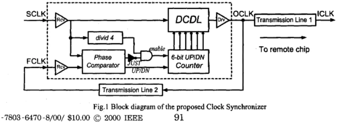
The block diagram of the proposed clock synchronizer is shown in Fig. 1 . It consists of an improved bang-bang type phase comparator, a set of control logic, a 6-bit up/down counter, a digital controlled delay line (DCDL)
and on-chip receivers and driver. A . Basic Principle
The main function of the clock synchronizer is to distribute the system clock to a remote chip. There should be as less skew as possible between the system clock and input clock. At first, a replica feedback path to the clock synchronizer itself having the same delay as the path to the remote chip is established on board. This makes both ICLK & FCLK to be in phase since AtLlnel is identical to AtLlnc~. Then the DCDL will be adjusted to change the phase of OCLK via the up/down counter so as to reduce the skew between SCLK and FCLK. The phase comparator will generate uP/DOWN signal to adjust the delay of DCDL. After both clocks are in phase, the total propagation delay from input clock to the feedback clock becomes a multiple of clock cycles (TcyCle). That is
At~cceiver + A~DCDL + At~nver + At~mne2 = m
*
Tcycle ( 1 ) Since Atllne2 = AtLlnel for two identical paths, this also makes the total propagation delay from SCLK to ICLK equal to an integer multiple of clock cycles. SCLK and ICLK become in phase after deskewing operation.A set of control logic including a divider and simple gates will determine the operating speed at one fourth of system clock frequency. These extra circuits will eliminate wrong result of phase comparison since there is a time difference (m* TcyClc) between SCLK and FCLK. While receiving the ‘JUST’ signal, the DCDL will stop adjusting its delay.
B.Phase Comparator
An improved phase comparator that consists of two traditional bang-bang type phase detectors[5] with a few extra logic gates is shown in Fig.2. When one clock speeds the other, either UP or DN signal will be generated. One may find there’s one unit delay added in front of the second phase detector. This will force this new phase comparator to generate a “JUST” signal when the phase difference of the two input clocks fall within one unit delay.
I
I
____.)
To remote chip
Fig. 1 Block diagram of the proposed Clock Synchronizer O-7803-6470-8/00/ $10.00
0
2000 IEEE91
The Second IEEE Asia Pacific Conference on ASICs / Aug 28-30, 2000 Then the “JUST” signal will disable the counter. The main
reason and benefit can be shown in later discussion about stability analysis. Thus, the unstable oscillatory phenomenon of DCDL phase can be eliminated. This can also reduce jitter at the clock buffer output.
UP SCLK
-
I I
I I
I I WJUST
DN
(a) Whole circuit
UP
dn
in2 vdd
*
-
.
(b) Bang-bang type phase detector Fig.2 Improved phase comparator
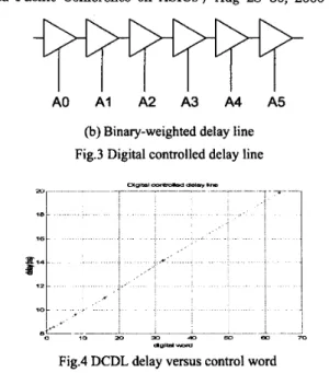
C. Digital Controlled Delay Line
A binary-weighted delay line with 6-bit upidown counter is used to adjust the phase of the output clock. As
shown in Fig.3, the delay path of each stage is determined by the counter output word. The capacitance, Ci, is well designed to satisfy the requirement of binary ratio in succeeding stages. The total delay of this DCDL is
AtDcDL = xi Ai X 2’ X KU -I- Atintrinsic
,
i = 0-
5 (2) where Ku is the unit delay and AGntrinsic is the delay throughthe multiplexors. The delay time of DCDL versus control word is shown in Fig.4. The Ku is 17Ops and the tuning range is up to llns. With only 6 stages, the DCDL will produce less jitter at its output effectively.
I I h
-I+
I 1 path-Lh r
(a) Basic structure of delay cell
A0 A I A2 A3 A4 A5
(b) Binary-weighted delay line Fig.3 Digital controlled delay line
_ L ._
I .
eL. ->
0 ~ 0 2 0 ~ 9 0 5 o m
**Id m
Fig.4 DCDL delay versus control word D. Stability Analysis
The stability of this clock synchronizer can be analyzed by using the block diagram in FigS. The phase comparator is modeled as the combination of a subtractor and a sign function. 8e represents the phase difference between system clock and feedback clock. The loop gain of DCDL is modeled as one unit delay Ku because DCDL is digitally controlled and only toggled at f l LSB (Ku). Since the system will measure the phase error 8e only after a time of an integer multiple of system cycles, the Z m represents the loop delay, e.g. m=l means one cycle delay. The close loop transfer function is
Ku
sign(&) x
- &Ku
zm+sign(&)x--1
& (3)H(z)
=To maintain the stability of a discrete-time system, the poles should be located within the unit circle of the z- plane. Then we may obtain loel > K d 2 for stable operation. For loel < Kd2, the system will become unstable and start to oscillate in its step response as shown in Fig. 6. Two simulation results with KU=~%*T,,~, and 10%*Tc,~, obtained from Matlab are shown in Fig.6. Since the phase error 8e will fall into the range of +xu12 at last, the improved phase comparator will generate a “JUST” signal to “open” the feed-forward path to maintain the phase error at a fixed value within f K d 2 while in- lock. This will reduce the system jitter effectively.
Fig. 5 Equivalent block diagram for stability analysis
92
Tal Run: Io.KGvx
r---
€ 1 Eampiei ' c
T - -
13 uar ipg8
es: u : s i
(a) Before synchronization TmRIx Run: I0.W
-1
N u m a r ~ l t w m ~ l w (b) Ku=IO%*T,,I~ Fig.6 Unit-step response 111.
EXPERIMENTAL RESULTS
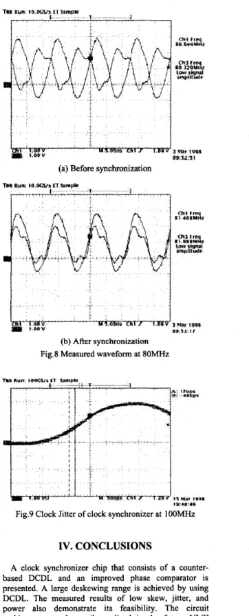
The proposed clock synchronizer chip has been fabricated in Holtek 0.8um SPDM CMOS process. The chip layout is shown in Fig.7. The die size is 2mm x 4mm including I/O pads. And the working voltage can be as low as 2 volts. Using a IO-inch transmission line and input clock range 40
-
125 MHz, the maximum skew is less than 400ps. The measured waveforms at 80MHz are shown in Fig.8. The peak jitter at IOOMHz is 17Ops as shown in Fig.9. The power consumption including an on-chip driver is only 25mW at 1 OOMHz.-Wi%ns CM
01.Sd. I ?
(b) After synchronization Fig.8 Measured waveform at 80MHz
t$:IW46
Fig.9 Clock Jitter of clock synchronizer at IOOMHz
IV. CONCLUSIONS
A clock synchronizer chip that consists of a counter- based DCDL and an improved phase comparator is presented. A large deskewing range is achieved by using DCDL. The measured results of low skew, jitter, and power also demonstrate its feasibility. The circuit architecture can be easily realized in the future VLSI
Fig. 7 Chip layout technology.
The Second IEEE Asia Pacific Conference on ASICs / Aug 28-30, 2000
ACKNOWLEDGEMENT
The authors would like to thank National Science Council for finance support and thank Holtek Inc. for the fabrication of the test chip. This work was sponsored by NSC87-2215-E002-031.
REFERENCES
[I] R. B. Watson, Jr. and R. B. Iknaian, “Clock buffer chip with multiple target automatic skew compensation,” IEEE J. Solid-state Circuits, vol. 30, pp. 1267-1276, Nov. 1995.
[2]H. Sutoh, K. Yamakoshi, and M. Ino, “Circuit technique for skew-free clock distribution,” IEEE Custom Integrated Circuits Con$, pp. 163-166. 1995 [3]M. G. Johnson and M. E. Hudson, “A variable delay
line PLL for CPU processor synchronization”, IEEE J. Solid-state Circuits, vol. 23, pp. 1218-1223, Oct. 1988.
[4]S. I. Liu, J. H. Lee and H. W. Tsao, “Low-power clock-deskew buffer for high-speed digital circuits,” IEEE J. Solid-state Circuits, vol. 4, pp. 554-558, Apr. 1999.
[5] J. Christiansen, “An integrated high resolution CMOS timing generator based on an array of delay locked loops”, IEEE J. Solid-state Circuits, vol. 31, pp. 952- 957, Jul. 1996.