High efficiency phosphorescent organic light-emitting devices with a
new organic material as the host of the emitting layer
Hsin-Hung Tsai
a, Jiun-Haw Lee
*a, and Man-Kit Leung
ba
Graduate Institute of Electro-Optical Engineering and Department of Electrical Engineering,
National Taiwan University, No. 1, Sec. 4, Roosevelt Road, Taipei, Taiwan, R.O.C.;
b
Department of Chemistry, National Taiwan University, Taipei, Taiwan, R.O.C
.
ABSTRACT
In this paper, we demonstrate a phosphorescent organic light emitting device (PHOLED) with low turn-on voltage by using a n-type organic material as the host of the emitting layer (EML) doped with green emitting complex, fac tris(2-phenylpyridine) iridium Ir(ppy)3. This material exhibits high glass transition temperature (over 200 oC) that may
help to elongate the operation lifetime. We compare our devices to the classical 4,4’-N,N’-dicarbazole-biphenyl (CBP) based green device. Driving voltage of the CBP and the new-host based OLED is 16 and 11 V with the current density of 100mA/cm2, respectively. The lower driving voltage of the new-host based device comes from the lower HOMO value, i.e. 5.7 eV, which is nearly the same as that of NPB. The current efficiency at 10000 cd/m2 is slightly decreased from 24 to 21 cd/A. However, the power efficiency is increased from 5 to 6 lm/W.
Keywords: OLED, phosphorescent
1. INTRODUCTION
High efficient phosphorescent light emitting diode (PHOLED) with carbazole based host materials has been demonstrated in recent years [1-3]. Due to the triplet state of metal-ligand charge transfer state (3MLCT) of fac
tris(2-phenylpyridine) iridium Ir(ppy)3 is between 2.5 and 3 eV , a suitable host material for efficient energy transfer is
necessary. Typically, 4,4’-N,N’-dicarbazole-biphenyl (CBP), is widely used as host materials of PHOLED since the peak wavelength of fluorophores is about 400 nm [4]. Thus, using (Irppy)3 in CBP can lead to efficient phosphorescent emission [5].
However, for the efficient energy transfer from host material to phosphor, the bandgap of host material is mostly large. The highest occupied molecular orbital (HOMO) value of CBP is about 6.3 eV which will result in a larger barrier for holes to inject from hole transmission layer (HTL) to emission layer (EML). Besides, Iridium based metal compounds are relatively more stable than the classical carbazole based host materials which is due to its low glass transition temperature (Tg). Thus, considering lower driving voltage and longer stability of device, the alternative for the host of PHOLED is required.
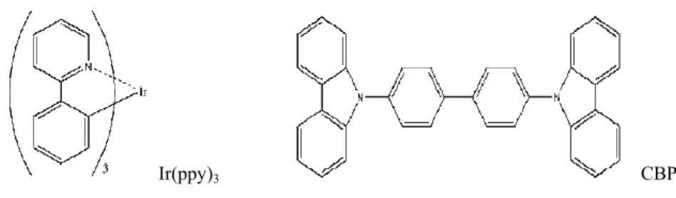
In this paper, we proposed a carbazole-free phosphorescent device by using a OXD based n-type materials which in rare and the result is far away form satisfactory [6]. As compared to the conventional CBP, this material shows a high glass transition temperature (over 200 oC) that may prolong the operation life time. Molecular structures of Ir(ppy)
3 and
CBPare shown in Fig. 1. In order to investigate the energy transfer of our phosphorescent system, we compared the PL (photoluminescence) of this materials and the absorption spectrum of Ir(ppy)3 and found the good spectrum overlap. We
also optimized this PHOLED with different concentration of Ir(ppy)3 and compared the operation life time with
carbazole based PHOLED.
Ir(ppy)3 CBP
Fig. 1 Molecular structure of Ir(ppy)3 and CBP.
2. EXPERIMENTS
In all of our devices, we used ITO glass substrate of low resistivity (10 Ohm/sqr) and flat surface roughness (Ra< 1nm). In order to lower ITO work function and clean ITO surface, we pretreated ITO surface with O2 plasma. All the
thermal evaporation of organic materials was in a batch-type chamber. The deposition rate was controlled at about 0.15 nm/sec and the chamber pressure is under 5x10⁻⁶ torr. As shown in Fig. 2, 40 nm
N,N’-diphenyl-N,N’-bis(1-napthyl)-1,1’-biphenyl-4,4’-diamine (NPB) was used as a hole transport layer (HTL). The emitting layer (EML) consisted of this host materials with different concentration of Ir(ppy)3 and CBP in our standard
device. 10 nm 2,9-dimethyl-4,7-diphenyl 1,10- phenanthrolin (BCP) was used as hole blocking layer and 30 nm tris-(8-hydroxyquinoline) aluminum acted as electron transport layer (ETL). The concentration of the Ir(ppy)3 is 0, 3, 5,
9, 15 % in the new-host based devices and 9% in standard device. After organic deposition, devices were exposed in atmosphere for about 20 seconds and delivered into glove box for encapsulation. The O2 and H2O concentrations of glove box are all below 10 ppm. Current-voltage characteristics of all devices were measured by using a Keithley 2400 source measurement unit. Brightness and emission spectrum was measured with Minolta CS1000 spectrophotometer. These instruments were connected to a personal computer and collaborated by software.
Fig. 2 Standard and compared device structures. The concentration of x is 0, 3, 5, 9, 15 % respectively
Al (150 nm)
LiF (0.1 nm)
Bebq2 (30 nm)
BCP (10 nm)
CBP : 9% Ir(ppy)
3(30
nm)
NPB (40 nm)
Al (150 nm)
LiF (0.1 nm)
Bebq2 (30 nm)
BCP (10 nm)
Host : x% Ir(ppy)
3(30
nm)
NPB (40 nm)
3. RESULTS AND DISCUSSIONS
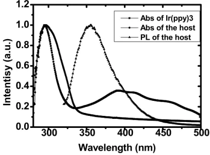
Figure. 3 shows the absorption and PL spectra of Ir(ppy)3 and the new-host based host. Phosphorescence proceeds
via either direct injection into the triplet metal ligand charge transfer state (3MLCT) or via inter system crossing (ISC)
from the singlet charge transfer state (1MLCT). In the figure, good spectrum overlap between the host emission (356 nm)
and the absorption of and the singlet metal-to-ligand charge-transfer state (1MLCT) of Ir(ppy)
3 (389.5 nm) has been
demonstrated. Thus, energy transfer from the host to Ir(ppy)3 seems possible.
300
350
400
450
500
0.0
0.2
0.4
0.6
0.8
1.0
1.2
In
te
nt
is
y
(
a.u.)
Wavelength (nm)
Abs of Ir(ppy)3 Abs of the host PL of the hostFig. 3 The absorption spectrum of the host and Ir(ppy)3 and PL of the host at room temperature.
Figure 4 shows current density and voltage curves (J-V) characteristics of host: x% Ir(ppy)3 and CBP : 9% Ir(ppy)3
devices. We can see that under the current density of 100mA/cm2, the driving voltage of the new-host and CBP based OLED is 11 and 16 V. Since the HOMO value of CBP is 6.3 eV which is lower than HTL material, NPB, the higher driving voltage is expected. However, since the HOMO value of our EML host is comparable to NPB, it results the lower driving voltage in these devices. With different dopant concentration, we can see that the driving voltage increases then decreases in the devices based on the new host. Here, we propose a model to explain this phenomenon. Since the host is a n-type material and Ir(ppy)3 is a kind of p-type molecule, holes (electrons) hop among the Ir(ppy)3 (the host) molecules in the EML. When the doping concentration is low, the distance between the Ir(ppy)3 molecules are large and it acts like a hole trap. Such a hole trap impedes further hole injection and the voltage increases. However, when the doping concentration increases, the hole mobility increases since the distance between the Ir(ppy)3 molecules decreases. Such an amipolar transport characteristics effectively decreases the driving voltage.
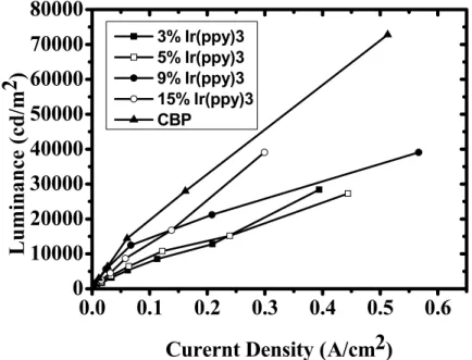
Figure 5 shows the luminance-current density characteristics of the new-host based device with different concentration of Ir(ppy)3 and Ir(ppy)3:CBP device. Compared the new-host: x% Ir(ppy)3 with different concentration
under the same voltage, 15% Ir(ppy)3 has the highest luminance of 15000 cd/m2 However, CBP: 9% Ir(ppy)3 has the
highest performance of luminance under the same current density. It seems that the better luminance can be attributed to more effective hole trapping on Ir(ppy)3.
0
2
4
6
8 10 12 14 16 18 20
0.0
0.2
0.4
0.6
0.8
1.0
Curre
nt De
ns
ity
(A/cm
2
)V (voltage)
0% Ir(ppy)3 3% Ir(ppy)3 5% Ir(ppy)3 9% Ir(ppy)3 15% Ir(ppy)3 CBPFig. 4 J-V characteristics for host: x% and CBP : 9% devices. The concentration of x is 0, 3, 5, 9, 15% respectively.
0.0
0.1
0.2
0.3
0.4
0.5
0.6
0
10000
20000
30000
40000
50000
60000
70000
80000
Luminance (
cd/m
2 )
Curernt Density (A/cm2)
3% Ir(ppy)3 5% Ir(ppy)3 9% Ir(ppy)3 15% Ir(ppy)3 CBP
Fig. 5 The luminance versus current density curves of Ir(ppy)3:the new-host and Ir(ppy)3:CBP device.
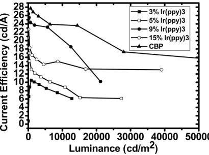
Figure 6 shows the result of current efficiency versus current density curves. For the new-host: x% Ir(ppy)3 devices,
9% Ir(ppy)3 has the highest current efficiency of 21 cd/A under the luminance of 10000 cd/m2. Although the luminance
of the new-host : 15% Ir(ppy)3 is higher than 9% Ir(ppy)3, the higher current density of 15% Ir(ppy)3 caused by more
efficient injection of holes through Ir(ppy)3 has the lower current efficiency. Comparing the optimized the new-host
than the new-host : 9% Ir(ppy)3.
0
10000 20000 30000 40000 50000
0
2
4
6
8
10
12
14
16
18
20
22
24
26
28
Current Efficiency (cd/A)
Luminance (cd/m2)
3% Ir(ppy)3 5% Ir(ppy)3 9% Ir(ppy)3 15% Ir(ppy)3 CBPFig. 6 Current efficiency versus luminance curves .
0
10000
2
4
6
8
10
12
14
P
o
wer Efficiency (lm/W)
Luminance (cd/m2)
the new host CBP
Fig. 7 Power efficiency versus luminance curves .
Figure 7 shows the power efficiency versus luminance characteristics. Due to the triplet-triplet annihilation at the interface between HBL and EML with increasing luminance, both the new-host and CBP based devices exhibit a gradual decrease in quantum efficiency. Besides, the higher power efficiency of the new-host based device can be explained in
terms of the lower driving voltage of the new-host based device.
4. SUMMARY
In conclusion, high stability and high efficiency carbazole-free phosphorescent OLED has been demonstrated, utilizing a multilayer architecture with BCP as the hole blocking layer. Driving voltage of the traditional CBP based device and the new-host based OLED is 16 and 11 V with the current density of 100mA/cm2, respectively. The lower driving voltage of the new-host based device comes from the lower HOMO value and good electron transport characteristics. The current efficiency at 10000 cd/m2 is slightly decreased from 24 to 21 cd/A. However, the power efficiency is increased from 5 to 6 lm/W.
REFERENCES
1. L. S. Hung, C. H. Chen, Materials Science and Engineering R 39 143-222 (2002). 2. L. S. Liao, K.P. Klubek and C. W. Tang, Appl. Phys. Lett. 84, 167 (2004). 3. C. Shen, I. G. Hill, A. Kahn, Adv. Mater. 11, 1523 (1999).
4. S. D. Wang, M. K. Fung, S. L. Lai, S. W. Tong, C. S. Lee, S. T. Lee, H. J. Zhang, and S. N. Bao, J. Appl. Phys. 94, 169 (2003).
5. J. Kido and T. Matsumoto, Appl. Phys. Lett. 73, 2866 (1998).
6. C. Adachi, M. A. Baldo, S. R. Forrest and M. E. Thompson, “High-efficiency organic electrophosphorescent devices with tris(2-phenylpyridine)iridium doped into electron-transporting materials,” Appl. Phys. Lett. 77, 904 (2000).