Low temperature chemical vapor deposition growth of
b
-SiC
on (100) Si using methylsilane and device characteristics
C. W. Liua)
Department of Electrical Engineering, National Taiwan University, Taipei 106, Taiwan
J. C. Sturm
Department of Electrical Engineering, Princeton University, Princeton, New Jersey 08544 ~Received 7 February 1997; accepted for publication 29 July 1997!
The growth properties of b-SiC on ~100! Si grown by rapid thermal chemical vapor deposition, using a single precursor ~methylsilane! without an initial surface carbonization step, were investigated. An optimun growth temperature at 800 °C was found to grow single crystalline materials. A simple Al Schottky barrier fabricated on n-type SiC grown on Si substrates exhibited a ‘‘hard’’ reverse breakdown of 13 V with a positive temperature coefficient of 231024°C21up to 120 °C, indicating an avalanche mechanism. A Pt Schottky barrier fabricated on n-type SiC grown on tilted Si substrates to improve the surface morphology exhibited a breakdown voltage of 59 V, with a negative temperature coefficient. From the analysis of the electrical field distribution, the breakdown probably occurred at interface defects between SiC and Si, as suggested by Raman spectroscopy. To investigate minority transport behavior, SiC/Si heterojunction bipolar transistors
~HBTs! were fabricated and compared to Si bipolar junction transistors. The collector currents of the
SiC/Si HBTs were similar to those of Si control transistors, because both devices had the same base structures. Compared to Si control transistors, the base currents of SiC/Si HBTs increased. It seems that the interface defects between Si and SiC act as recombination centers to deplete back-injected holes, instead of being the barrier to stop hole currents, and thus to increase the base currents of SiC/Si HBTs. © 1997 American Institute of Physics.@S0021-8979~97!03921-2#
I. INTRODUCTION
The unique thermal and electronic properties of SiC make it a promising material for electronic and optoelec-tronic devices designed to operate in extreme conditions such as high voltage, high temperature, high frequency, and high radiation. SiC has many different one-dimensional polytypes ~different stacking sequences!. A repetitive ABC stacking sequence yields a zincblende structure, referred to as 3C orb-SiC. The other about 170 non-cubic crystals are referred to as the a-SiC family. Recently, most of the re-search activities and progress have been made on a-SiC, primarily 6H and 4H,1,2 because of the mature bulk crystal technologies.3There are no suitable substrates ofb-SiC crys-tals, but b-SiC epilayer has been grown in the past on Si
~100! substrates, despite a 20% mismatch of lattice constants
and an 8% mismatch of thermal expansion coefficients be-tween b-SiC and Si. Conventionally, the chemical vapor deposition growth ofb-SiC on Si requires high growth tem-peratures (>1300 °C!4 using separate precursors such as SiH4 for Si and C3H8 for C, and an initial high temperature
surface carbonization step,5,6 which prevents the possibility of integration with silicon-based devices. Furthermore, the low material quality is reflected in very leaky Schottky bar-riers with the highest reported soft breakdown of only 8–10 V.7 In this study, we report growth properties of cubic SiC on ~100! Si grown at temperature as low as 700 °C using a single gas precursor ‘‘methylsilane’’ without the carboniza-tion step, first demonstrated by Golecki et al.8We describe the material properties of the films using x-ray diffraction,
Raman scattering, Fourier transform infrared absorption, and transmission electron microscope, and then discuss Schottky barriers and Si/SiC heterojunction bipolar transistors fabri-cated on these films.
II. GROWTH
Due to the lack of suitableb-SiC substrates,b-SiC was grown on Si~100! substrates. The SiC films were deposited on tilted ~4° towards
^
110&
) and nontilted Si substrates~within 1° off! with a diameter of 100 mm by rapid thermal
chemical vapor deposition ~RTCVD! at a growth tempera-ture of 700–1100 °C. The growth pressure was 1 Torr with a 1.5 sccm methylsilane~SiCH6) flow and a 500 sccm hydro-gen flow. The growth temperature ~700–800 °C! was accu-rately determined by the infrared transmission technique.9 Growth temperatures higher than 800 °C were controlled by the tungsten-halogen lamp power which was previously cali-brated with a thermocouple welded onto a Si wafer. The SiC thickness was measured by fitting the optical reflection spec-tra from 500 to 700 nm with the SiC index of refraction of 2.6. Since the temperature is not uniform across the wafer
~the edge is about 50 °C lower than the center!, the thickness
was measured at the spot very close to the position where the temperature was monitored ~near the center of the wafer!. Figure 1 gives the Arrhenius plot of the growth rate of SiC on nontilted ~100! Si. The growth rate in the range 700– 800 °C varied exponentially with the inverse of temperature and the activation energy for this surface-reaction-limited growth was 3.6 eV. This is higher than that of pure silicon growth using silane as a precursor (;1.7 eV!10 and may reflect the strong C–H bonding energy. At a higher growth
temperature~800–1100 °C!, the growth rate had a weak tem-perature dependence, indicating mass-transport-limited growth.
The crystallinity of the films was studied by x-ray dif-fraction ~XRD! and transmission electron microscope
~TEM!. For the films grown at 750 °C, the XRD spectrum @Fig. 2~a!# of an 80 nm film on nontilted substrates exhibited
a single crystalline feature with a broad unresolved Cu Ka1 and Cu Ka2 ~400! peak @full width half maximum ~FWHM! of 2u is about 1.6°]. But the TEM diffraction pattern @Fig. 2~b!# of the same sample showed evidence of some slightly in-plane rotated textures and very fine spots in the
^
110&
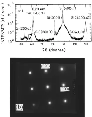
direction. This indicates the poor crystallinity of the 750 °C films. The crystallinity can be improved by increasing the growth temperature to 800 °C. The XRD spectrum @Fig. 3~a!# of a 0.23mm SiC film grown at 800 °C on nontilted substrates showed that the FWHM of unresolved Cu Ka~400! peak was as small as 0.75°, which was similar to the
value ~0.65–0.7°! of 0.3 mm commercial~100! SiC on Si,8 which was grown at a much higher temperature~>1300 °C!. The TEM diffraction pattern @Fig. 3~b!# also displayed a well-defined single crystalline feature. The films grown at 800 °C on tilted substrates had similar XRD spectra and TEM diffraction patterns, but had relatively smoother sur-face morphologies, compared to nontilted substrates, as ob-served under the optical microscope. This facilitated the Schottky barrier fabrication on tilted substrates to reduce leakage current. TEM also showed very high densities of stacking faults and dislocations, similar to films of similar thickness grown by conventional high temperature growth techniques. The Fourier transform infrared~FTIR, not shown here! spectra of a 0.23 mm 800 °C grown film on nontilted substrates displayed an absorption peak at 796 cm21 ~TO phonon absorption! with a FWHM of 50 cm21, which is similar to that of the film grown by conventional high tem-perature growth methods.11The Raman spectrum~Fig. 4! of the same sample showed a broad peak at 960 cm21 with FWHM of 60 cm21 and a sharp peak 510 cm21. The 510 cm21 peak is associated with the Si substrates, not SiC ep-ilayers. The peak near 960 cm21 is probably due to a
com-FIG. 1. Arrhenius plot of the growth rate of SiC on nontilted~100! Si. Note
that the phosphorus incorporation decreases the growth rate.
FIG. 2. The XRD spectrum~a! and TEM diffraction pattern ~b! of a 750
°C-grown film with a thickness of 80 nm.
FIG. 3. The XRD spectrum~a! and TEM diffraction pattern ~b! of a 800
bination of the LO phonon scattering ~;970 cm21) and in-terface defects between SiC and Si.12The XRD spectrum of the film grown at 1000 and 1100 °C, however, reveals extra
~111! and ~220! peaks, indicating the growth of
polycrystal-line material. Therefore, the 800 °C is the optimum growth temperature for the single crystallineb-SiC. However, ‘‘two step growth,’’ namely, a thin layer grown at 800 °C first, followed by high temperature growth, can improve the single crystallinity of the films. For example, a film with a thick-ness of 0.45 mm grown at 1000 °C formed a polycrystalline structure@Fig. 5~a!# However, if a 0.15mm layer was depos-ited at 800 °C, followed by a 0.3mm film grown at 1000 °C, this improved the single crystalline quality of the layers grown at 1000 °C@Fig. 5~b!#. This shows that a low growth temperature ~800 °C! at the SiC/Si interface is essential for the growth of single crystalline layers by this technique, in contrast to what is often obsered in conventional growth techniques which require high growth temperatures and sur-face carboninzation at the SiC/Si intersur-face to improve crystallinity.
III. DOPING
Unintentionally dopedb-SiC layers always show n-type conduction.13Although there was some controversy initially,
there appears to be agreement that the origin of the n-type conduction is controlled by a shallow donor~nitrogen! with a binding energy of 15–20 meV.13Note that nitrogen source in our growth system is thought to come from the methylsilane gas precursor, which was only 99% pure. Nitrogen was also commonly used as the n-type dopant inb-SiC. On the other hand, very limited studies of phosphorus-doped SiC have been reported. The p-type dopant of Al is popularly used to obtain p-type SiC, because of its relatively low acceptor binding energy of 0.24 eV, compared to boron with the value of 0.735 eV. In this work, we investigate the in situ incorpo-ration of boron and phosphorus into b-SiC.
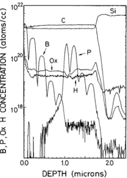
The boron and phosphorus incorporation are accom-plished by introducing diborane ~10 ppm in hydrogen! and phosphine ~70 ppm in hydrogen! precursors, respectively, into gas mixtures. Their incorporation into 800 °C grown b-SiC layers was measured by secondary-ion mass spectros-copy @SIMS, ~Fig. 6!# on a multilayer sample with various dopant gas flows. Each doped layer was grown for 10 min and separated by unintentionally doped spacers grown for 5 min. We did not perform systematic study of the residual dopant effect on the undoped spacers, but the undoped spac-ers seemed to work well to separate the adjacent doped lay-ers. For SiGe layers grown in the same chamber, the turn-off slope of phosphorus doping in the doped SiGe was about 300 Å/decade from 331018to 1017cm23. Both boron and phos-phorus showed approximately linear incorporation with the gas flow up to the concentrations of 531020 and 331020 cm23 for boron and phosphorus, respectively ~Fig. 7, com-piled from SIMS data!. No systematic Hall measurements or direct electrical activation measurements versus dopant level was performed. The SIMS data also indicated that there were large amounts of oxygen and hydrogen contamination in our SiC films grown at 800 °C with the concentrations of
FIG. 4. The Raman spectrum of of a 0.23mm 800 °C grown film.
FIG. 5. The XRD spectra of a 1000 °C grown film with a thickness of 0.45
mm~a! and a ‘‘two-step’’ film ~b!. A 0.15mm layer was deposited at 800 °C
first, then followed by a 0.3mm layer grown at 1000 °C for the ‘‘two-step’’
film.
FIG. 6. A SIMS plot of SiC multilayers with impurity incorporations. The growth temperature was 800 °C except the top layer. The bumps are the
doped layers with different phosphine~or diborane! flows. The valleys are
the undoped spacers. Note that the top layer was a diborane-doped film grown at 750 °C.
331019and 231019cm23, respectively. One interesting ob-servation is that phosphorus incorporation with high phos-phine to methylsilane flow ratio ~;1.231022, correspond-ing chemical concenration of 331020 cm23) reduced the growth rate of SiC by a factor of 10 and 5 for the growth temperatures of 800 and 750 °C, respectively~Fig. 1!. SIMS
~Fig. 6! also showed that the width of the highest peak in the
P profile with the phosphine to methylsilane flow ratio of 331022becomes narrower~indicating a slower growth rate! as compared with other phosphorus doped layers with lower phosphine flow rates. A suppressed growth rate due to phos-phine incorporation has also been reported in Si epitaxial growth.14Boron incorporation can be utilized to compensate the background impurities of the SiC films. This increases the breakdown voltage of Schottky diodes fabricated on SiC films as shown in Sec. IV.
IV. SCHOTTKY BARRIERS
The SiC grown on Si by conventional high temperature techniques has various kinds of defects, which cause very leaky diodes with soft breakdown voltage less than 10 V.7 Although the~111! b-SiC grown on 6H SiC has been dem-onstrated with a hard breakdown voltage of 200 V,15 the temperature coefficient of breakdown voltage is negative, which is contradictory to the avalanche process. Therefore, we fabricated Schottky barriers on~100!b-SiC grown on Si to study the reverse breakdown characteristics, using this low temperature growth technique. The samples used for Schottky barriers were grown at 800 °C. Since the uninten-tionally doped SiC films were n-type with carrier concentra-tions around 1018 cm23 or higher as determined by Hall measurement, boron compensation was necessary to reduce the net dopant concentration of SiC films. The chemical con-centration of boron used for this purpose was about 1020 cm23 ~measured by SIMS in samples grown under similar conditions!. However, most boron might be located in non-electrically active interstitial sites.16 The electrically active acceptor concentration is estimated about 1% of the chemical concentration.17Therefore, the active acceptor concentration was the same order of magnitude of the background donor
concentration. To get the least amount of net dopant concen-tration in the SiC layers, sometimes we grew a series of films with different B2H6 flows, and then picked the best diodes
fabricated from those films. Before metal evaporation, the boron-compensated n-type SiC films were cleaned in dilute HF without any extra polishing, oxidation, and etching.7The size of Schottky barriers was defined either by photolithog-raphy or by shadow masks. Two kinds of Schottky barrier structures were studied:
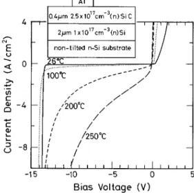
~a! Al ~500 nm! Schottky barriers of size 1.331024cm2
were fabricated on 0.4mm, 2.531017cm23n-type SiC, with a 2mm, 131017cm23, n-type Si buffer on nontilted Si~100! n-type substrates as shown in the insert of Fig. 8.
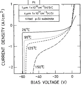
~b! Pt ~80 nm! Schottky barriers of size 1.331023 cm2
were fabricated on 1 mm, 131016cm23, n-type SiC with 4
mm, 131017 cm23, n-type Si buffers, but on tilted p-type substrates as shown in the insert of Fig. 9.
Because of the rough morphology of thick layers (. 0.5 mm! grown on non-tilted substrates, the structure ~b! was grown on tilted substrates~4° toward
^
110&
) to get a smooth morphology, which reduced the leakage current of the Schottky diodes. The Al was deposited by a thermal evapo-rator. The Pt evaporation was performed by an electron beam evaporator. Instead of being held at elevated temperature,18 our samples were not intentionally heated during Pt evapo-ration. The net dopant concentrations of SiC were measured by capacitance-voltage (C – V) measurement after the Schottky barriers were made.The diodes were measured by current-voltage (I – V) and high frequency C – V at 1 MHz in a light-tight box. One probe made contact to the Schottky barrier itself and the other to a large metal contact away from the barrier. Since both contacts are on the same side of the wafer, the diodes have large series resistance, which has serious effect on for-ward I – V characteristics in terms of ideality factors. We therefore only focused on the reverse breakdown behaviors and made comparison to previous results. The reverse I – V
FIG. 7. The chemical concentrations of dopant~P and B! in SiC as a
func-tion of ratio of actual dopant flow to methylsilane flow at a growth tempera-ture of 800 °C.
FIG. 8. The I-V characteristics of Al Schottky barriers. The insert is the device structure. A positive temperature coefficient was observed for the reverse breakdown voltage.
characteristics of the Al Schottky barriers@structure ~a!# had a hard breakdown voltage of 13 V ~Fig. 8!. To avoid the effect of reverse leakage current, the value of breakdown voltage is obtained by extrapolating the current at breakdown to the x axis~voltage axis!. The depletion depth at the break-down was about 0.22mm obtained from the C – V measure-ment ~Fig. 10!, and was completely confined in the SiC layer. The breakdown electric field calculated from break-down voltage and doping concentration was 13106 V/cm, about one third of the theoretical value for b-SiC.19 The reduction compared to the ideal value is possibly due to the defects of the SiC lattice using this growth method. The tem-perature coefficient of breakdown voltage showed a positive value of about 231024°C21 from room temperature to 120 °C, and became negative above 190 °C with soft break-down. Unlike the previous reported negative value15 for Schottky barriers on b-SiC heteroepitaxially grown on 6H SiC, this is the first observation of a positive temperature coefficient of breakdown voltage in b or a-SiC grown by any method. Such a positive temperature coefficient is highly desirable in device applications to prevent runaway if de-vices reach the breakdown point. This also indicates that
impact ionization avalanche transit time ~IMPATT! diodes can possibly be made in b-SiC, because the positive tem-perature coefficient is the direct result of an impact ioniza-tion process,20 required for the IMPATT diodes. Combined with the high electron saturation velocity ~two times of Si value!, the IMPATT diodes based on the b-SiC material might reach an oscillation frequency of 200 GHz. The Al Schottky barriers showed the same I – V characteristics after annealing at 500 °C for 10 min in a forming gas without any degradation.
The reverse I – V characteristics of Pt Schottky barriers in Fig. 9 showed 59 V breakdown voltage, and the depletion depth at breakdown was 2.5 mm obtained from C – V mea-surement~Fig. 11!, implying that the entire SiC layer ~1mm! was depleted and the depletion region terminated in the n-type Si layer. The electric field in SiC and Si, calculated from Poisson’s equation and doping profile obtained from C – V, did not reach the breakdown field of either SiC (13106 V/cm! or Si (;63105 V/cm!. The breakdown
probably occurred at the interface defects between SiC and Si due to the misfit of lattice constants and thermal expan-sion coefficients, the presence of which were suggested by Raman spectroscopy. Recently, there was a report that the oxygen in the gas mixture also formed voids at the SiC/Si interface.21 The defects and voids between the SiC and Si interface probably lowers the breakdown electrical field of the avalanche process. Note that since the breakdown voltage
~59 V! is much larger than the 6Eg/q (Eg is the band gap,
2.2 eV, and q is the electron charge!, the breakdown is an avalanche process.20 The temperature coefficient of break-down voltage had a negative value of 431024 °C21 from room temperature to 120 °C. The Pt Schottky barriers de-graded after forming gas annealing at 500 °C for 10 min, showing a soft breakdown around 10 V. This is contrary to the results of Ref. 18, where the Pt Schottky barriers showed improved reverse I – V characteristics at a reverse bias of a few volts after isochronal annealing. This controversy may be ascribed to the breakdown in the Si/SiC interface of our Schottky barriers, instead of in the bulk SiC. The breakdown voltage should be improved by using the n1-SiC layer below the active SiC layer to terminate all the electric field lines FIG. 9. The I-V characteristics of Pt Schottky barriers. The insert is the
device structure.
FIG. 10. The depletion depth as a function of reverse bias voltage for an Al
Schottky barrier. The depletion depth at breakdown was about 0.22mm.
FIG. 11. The depletion depth as a function of reverse bias voltage for a Pt
Schottky barrier. The depletion depth at breakdown was about 2.5mm and
before the field lines reach the interface. Please note that the reverse saturation currents of Al and Pt barriers are 631022 and 0.3 A/cm2, respectively, which are much higher than the b-SiC pn diodes grown on 6H SiC in Ref. 15, but the origin is not clear.
The barrier heights of both barriers can be obtain from the expression:
Fb5Vi1z2DF1kT/q,
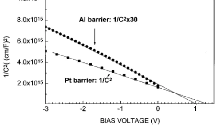
where Viis the intercept of 1/C2vs V plots~Fig. 12!,zis the
difference between conduction-band edge and Fermi level,
DF is the image force lowering, and kT/q is the thermal
voltage. Using the z andDF values in Ref. 18, the barrier heights of Pt and Al barriers are 1.4 eV and 1.1 eV, respec-tively. The Pt barrier height agrees well with the previous reported value ~1.35 eV!,18 while a higher value ~1.69 eV! was reported on~n11! orientation.16The barrier height of Al barriers, which were deposited in an ultrahigh-vacuum chamber, was estimated as 1.4 eV by the photoemission method.22
V. HETEROJUNCTION BIPOLAR TRANSISTORS
Despite the success with Si/SiGe/Si HBTs, there is still a strong desire for a wide gap emitter material on Si. Such a wide gap emitter on a Si base could yield devices with better high temperature performance than Si/SiGe HBTs ~due to higher band gap! and might be easier to be integrated.23The high current gain in a wide band gap emitter HBT may be also traded for low base resistance. This low base resistance, combined with a short base transit time in a very thin base, will produce transistors of high speed performance compat-ible with existing polysilicon-emitter technologies. Several materials such as semi-insulating polycrystalline Si~SIPOS!, amorphous Si, GaP, and b-SiC have been reported to serve this purpose.24 A current gain of 800 has been obtained by b-SiC grown by a special technique at 1000 °C on~111! Si substrates.25 However, the high temperature process of 1000 °C would produce excessive back diffusion and prevent the integration with other Si devices. The band gap ofb-SiC is 2.2 eV, but the band alignment between b-SiC and Si is not known.
The single crystallineb-SiC grown at 800 °C on~100! Si substrates was used for the wide band gap emitter material of Si/SiC HBTs. Figure 13 displays the layer structures of a Si control device ~Si bipolar junction transistors! and a SiC/Si HBT. In the SiC/Si HBT, there is an additional 2000 Å un-intentionally doped SiC layer (n51018 cm23) between the n-Si emitter and the n1-Si emitter. Note that the n1-Si emit-ter grown on the SiC layer in the SiC/Si HBT structure was polycrystalline, confirmed by x-ray diffraction. The heavily doped base ( p51019 cm23) is designed to increase the
maximum frequency of oscillation by reducing the base sheet resistance. To avoid the tunneling current in the emitter junction, a 0.3 mm moderately doped Si emitter (n51017 cm23) was grown, followed by the heavily doped emitter layers.26The thickness of the n-type Si emitter is small com-pared to the hole diffusion length, which is estimated to be about 10mm for hole mobility of 330 cm/V s and life time of 0.1 ms. Therefore, the hole diffusion in the emitter will be affected by the boundary condition at the SiC/Si interface. Note that Si/SiGe/Si HBTs with a record-high maximum fre-quency of oscillation of 160 GHz have used this structure of a heavily doped base and a moderately doped Si emitter followed by a heavily doped emitter layer.27 Similar doping or structural profiles were used in Refs. 28–30. As a result, the depletion width of the emitter varied from 1100 to 600 Å as the emitter-base voltage varied from 0 to 0.7 V, within the moderately doped Si emitter, while the depletion width in the heavily doped base varied from 110 from 60 Å. However, the interface between SiC and Si is defective due to the 20% misfit, the emitter junction of SiC/Si HBTs is designed in the Si/Si pn junction, instead of the Si/SiC pn junction, to avoid
FIG. 12. The 1/C2vs bias voltage plots for Pt and Al Schottky contacts on
b-SiC.
FIG. 13. Layer structures of a Si bipolar junction transistor and a SiC/Si heterojunction bipolar transistors. There is an additional SiC layer between
the recombination current in the delpetion region of the emit-ter junction. There might be two main effects of the SiC layer in the emitter on device performance. The desired one is that the n-SiC layer can block back-injected hole current
~base current! as a diffusion barrier and thus increases the
current gain. This is similar to poly-Si BIJs.23An undesired effect is that the defective SiC/Si interface might act as a recombination center for hole current and thus decrease the current gain. The defect density of Si/SiC interface will de-termine which effect is larger. The transistors were fabri-cated using a double-mesa process, which was detailed in Refs. 31 and 32. The base contact was established by boron implant. Before base implantation, the emitter mesas were formed by plasma etching~SF6for Si and 8% O2 in CF4for SiC!. The devices were isolated by plasma-etched mesas and passivated with SiO2 deposited by plasma deposition at 350 °C. Before contact metallization, the wafers were given a RCA clean, and annealed at 700 °C for 30 min in a forming gas. The emitter size was 60mm360mm for both HBTs and BJTs.
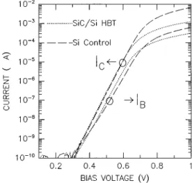
Figure 14 shows the base current and collector current as a function of the emitter-base voltage ~Gummel plot!. The collector-base voltage is fixed at 2 V. The collector currents for both devices showed same voltage (Vbe) dependence
with an ideality factor of 1.0 and the same absolute magni-tude. This result is expected, because both devices have the same base structures and the same barriers for electron trans-port from the emitter to the collector. The base currents also showed near-ideal behavior with ideality factors of 1.2 and 1.1 for Si BJTs and SiC/Si HBTs, respectively. However, the desired enhancement of current gain (Ic/Ib) was not
ob-served, because the base currents of SiC/Si HBTs was higher than those of Si BJTs. For example, the current gains are 3.7 and 7.7 for HBTs and BJTs, respectively, at the emitter base voltage of 0.6 V. The current gains (Ic/Ib) of both devices
are also shown in Fig. 15 and the Si BJT has higher current gain than the SiC/Si HBT at high collector current. The in-crease of base currents in the SiC/Si HBT’s, compared to the
Si BJT’s, indicated that the interface defects between Si and SiC acted as recombination centers for back-injected holes. Therefore, the back-injected holes recombined at the SiC/Si interface. The wide band gap SiC layer would be a barrier to stop the hole current if the interface defects were removed and there was no recombination hole current at the SiC/Si interface. Moreover, the fact that the base current is domi-nated by hole diffusion current in the neutral emitter is con-firmed by the ideality factor of base currents. If the base hole currents were from the recombination in the depletion region of emitter junction, the ideality factor should be the same for both HBTs and BJTs, since both depletion regions were within the n-type Si emitters. However, a more ideal base current was observed in the HBTs (n51.1) than in the BJTs (n51.2). This indicates that the dominant base current oc-curs in a neutral emitter region in the HBTs and not in a depletion region or a device edge ~surface!. Note also the apparent high series resistance of the HBTs. This is thought to result from the SiC layer in the emitter. The SiC/Si HBT did not increase the current gain compared to the Si BJT due to the defective interface. To reduce the defect density at the interface, a passivation technology of the interface will be desired in the future.
VI. SUMMARY
A single crystallineb-SiC has been grown at 800 °C on Si. The growth temperature of 800 °C was essential for ini-tial single crystalline SiC layers on Si ~100! substrates. Schottky barriers on n-type SiC on~100! Si showed a hard reverse breakdown voltage as high as 59 V. A positive tem-perature coefficient of breakdown voltage of SiC was ob-served for the first time with the breakdown voltage of 13 V. The density of interface defects should be further reduced for desired SiC/Si HBT performance.
ACKNOWLEDGMENTS
The TEM assistance of Dr. E.A. Fitzgerald of ATT Bell Labs and Professor P. Pirouz and Dr. J. W. Yang of Case Western Reserve University, and the SIMS analysis of Dr. C. W. Magee of Evan East are gratefully appreciated. The sup-port of the U.S. Office of Naval Research ~Grant No. FIG. 14. The Gummel plots of a SiC/Si HBT and a Si control device. The
base current of theb-SiC/Si HBT was higher than that of the Si control
device, while the collector currents for both devices were very similar due to identical base structures of these two devices.
FIG. 15. The current gain vs collector current plots for Si BJTs and Si/SiC HBTs.
N000121-90-J-1316! is gratefully acknowledged. One of the authors~C.W.L.! would like to thank the support of the Na-tional Science Council of the Republic of China under Con-tract No. 85-2215-E-005-002 for publishing this article.
1M. Bhatnagar, B. J. Baliga, H. R. Kirk, and G. A. Rozgonyi, IEEE Trans.
Electron Devices 43, 150~1996!.
2
C. Schroder, W. Heiland, R. Held, and W. Loose, Appl. Phys. Lett. 68, 1957~1996!.
3Y. M. Tairov and V. F. Tsvetkov, J. Cryst. Growth 52, 146~1981!.
4P. Liaw and R. F. Davis, J. Electrochem. Soc. 132, 642~1985!.
5
S. Nishino, Y. Hazuki, H. Matsunami, and T. Tanaka, J. Electrochem.
Soc. 127, 2674~1980!.
6S. Nishino, J. A. Powell, and H. A. Will, Appl. Phys. Lett. 42, 460~1983!.
7D. E. Ioannou, N. A. Papanicolaou, and P. E. Nordquitst, IEEE Trans.
Electron Devices 34, 1694~1987!.
8
I. Golecki, F. Reidinger, and J. Marti, Appl. Phys. Lett. 60, 1703~1992!.
9J. C. Sturm, P. V. Schwartz, E. J. Prinz, and H. Manoharan, J. Vac. Sci.
Technol. B 9, 2011~1991!.
10J. L. Regolini, D. Bensahel, J. Mercier, and E. Scheid, Appl. Phys. Lett.
54, 658~1989!.
11
J. P. Li, J. Steckl, I. Golecki, and F. Reidinger, Appl. Phys. Lett. 62, 3135
~1993!.
12Z. C. Feng, A. J. Mascarenhas, W. J. Choyke, and P. A. Powell, J. Appl.
Phys. 64, 3176~1988!.
13
J. A. Freitas, S. G. Bishop, P. E. R. Nordquist, and M. L. Gipe, Appl.
Phys. Lett. 52, 1695~1988!.
14M. L. Yu, D. J. Vitkavage, and B. S. Meyerson, J. Appl. Phys. 59, 4032
~1986!.
15
P. G. Neudeck, D. J. Larkin, J. E. Star, J. A. Powell, C. S. Salupo, and L.
G. Matus, IEEE Electron Device Lett. 14, 136~1993!.
16
R. F. Davis, G. Kelner, M. Shur, J. Palmour, and J. A. Edmond, Proc.
IEEE 79, 677~1991!.
17H. J. Kim and R. F. Davis, J. Electrochem. Soc. 133, 2350~1986!.
18
N. A. Papanicolaou, A. Christou, and M. L. Gipe, J. Appl. Phys. 65, 3526
~1989!.
19
M. Bhatnagar and B. J. Baliga, IEEE Trans. Electron Devices 40, 645
~1993!.
20S. Sze, Physics of Semiconductor Devices~Wiley, New York, 1981!, pp.
98 and 566.
21A. Leycuras, Appl. Phys. Lett. 70, 1533~1997!.
22
V. M. Bermudes, J. Appl. Phys. 63, 4951~1988!.
23T. K. Ning and D. D. Tang, Proc. IEEE 74, 1669~1986!.
24S. Sze, High-Speed Semiconductor Devices~Wiley, New York, 1990!, p.
366.
25T. Sugii, T. T. Ito, Y. Furumura, M. Doki, F. Mieno, and M. Maeda, IEEE
Electron Device Lett. 9, 87~1988!.
26Z. Matutinovic-Krstelj, E. J. Prinz, P. V. Schwartz, and J. C. Sturm, IEEE
Electron Device Lett. 12, 163~1991!.
27A. Schuppen, U. Erben, A. Gruhle, H. Kibbel, H. Schumacher, and U.
Konig, Tech. Dig. Int. Electron. Device Meet. 743~1995!.
28E. J. Prinz, P. M. Garone, P. V. Schwartz, X. Xiao, and J. C. Sturm, IEEE
Electron Device Lett. 12, 42~1991!.
29S. S. Lu, C. C. Wu, C. C. Huang, F. Williamson, and M. I. Nathan, Appl.
Phys. Lett. 60, 2138~1992!.
30H. R. Chen, C. P. Lee, C. Y. Chang, J. S. Tsang, and K. L. TSai, J. Appl.
Phys. 74, 1398~1993!.
31L. D. Lanzerotti, A. St. Amour, C. W. Liu, J. C. Sturm, J. K. Watanabe,
and N. D. Theodore, IEEE Electron Device Lett. 17, 334~1996!.
32Z. Matutinovic-Krstelj, V. Venkataraman, E. J. Prinz, and J. C. Sturm,