國立交通大學
電子物理研究所
碩士論文
氮化銦奈米粒之成長與特性分析
Growth and characterizations of InN
nanodots
研究生:傅少甫
指導教授:陳衛國 教授
氮化銦奈米粒之成長與特性分析
Growth and characterizations of InN
nanodots
研究生:傅少甫 Student: Shao-Fu Fu
指導教授:陳衛國 教授 Advisor: Prof. W. K Chen
國立交通大學 電子物理研究所
碩士論文
A Thesis
Submitted to Institute of Electrophysics College of Science
National Chiao Tung University In Partial Fulfillment of the Requirements
In
Electrophysics August 2007
致謝
短短兩年的時間在我的一生卻恍如隔世阿,熬到最後一天終於得 到老師的簽名一枚,這一切的處心積慮還不是為了那一張紙,首先我 要先跟曾經坐我旁邊的人致歉,他們輕則休學重則殘疾,為了都是成 就我的碩士論文。當然也要感謝我的指導教授陳衛國老師指導有方, 對論文的細心指導外也給我莫大的鼓勵。讓我肯拋開一切踏入火坑, 另外,也要感謝團隊中的李明知老師、周武清老師和張文豪老師,給 我相當寶貴的意見,才能讓我完成這篇論文。 再者,要感謝實驗室的里長伯京玉學長,對我的研究上助益良 多,包辦我的吃喝拉撒,還要謝謝大內總管實驗室最德高望重的妮妮 學長,和實驗室光學一哥文哲學長率領的光學團隊大力相助,以及熱 愛網拍的林萱學姊,以及實驗室跟著我一起接受人體極限的夥伴們, 在我左右首先被我克走的仲葳和離家出走的峰毅,還有實驗室我的好 姐妹老被大家寫錯名字的沛雯,沒有你那有我們的阿桑團隊,還有老 講冷笑話的書鴻,以及給我幫忙很大的老包和 DESK,謝謝你們讓實 驗室充滿了歡樂,還有學弟家賢、聖允(雖然我一開始總誤會你會和 家賢在一起),以及超熱血的阿德和毛頭,並且被我拐進實驗室的我 的阿馬,有你讓我深活充滿了樂趣。的時候也有溫暖的避風港,還要感謝姊姊的加油打氣,當然還有父親 和弟弟。還有在這個實驗室讓我學到,努力不一定有好結果,但不努 力一定死的超難看。
Index
A b s t r a t e ( C h i n e s e Ve r s i o n ) … … … . … … … i
Abstrate(English Version) ……….………..…iii
C h a p t e r 1 I n t ro d u ct i o n … … … . … … … . . . … … 1
Chapter 2 Theoretical Backgrounds………….………...…...5
2-1 Dot growth mechanisms………….………...…...5
2-2 InN structure………….………...…...10
2 - 3 P h o t o l u m i n e s c e n c e … … … . . . … . . . 1 2 Chapter 3. Experiments………….………...…...15
3.1 Sample preparation……….………...………...17
3.2 Atomic force microscopy (AFM)……….20
3.3 Photoluminescence (PL) ……….….23
Chapter 4 Results and discussion……….…..25
4.1 Critical thickness………...………….…..25
4.2 Surface morphology of InN dots………...………….…..29
4.3 Bimodal distribution of InN islands on GaN ………...…..33
4.4 Vicissitudes of two shapes of InN dots………...…..39
4 . 5 P L r e s u l t s … … … . . 5 0 Chapter 5 Conclusion………...…..53 R e f e r e n c e … … … . . 5 6
氮化銦奈米粒之成長與特性分析
研究生:傅少甫 指導教授:陳衛國 博士
國立交通大學
電子物理研究所
中文摘要
本篇論文主要是利用原子力顯微鏡(AFM)及螢光光譜
(PL)等實驗技術來研究關於 InN 奈米粒(nano-dots)在不同
覆蓋厚度(coverages)的過程中的長晶動力學,以及對形貌
和發光特性的研究。
利用原子力顯微鏡,我們觀察到以 MOCVD 的方式成長 InN
奈米粒在 650
o時會呈現兩種不同形貌的奈米粒,分別為平頂
(flat-top)和圓頂(dome-shape)的奈米粒,並且隨著覆蓋的
厚度改變時,兩種不同形貌的奈米粒會有所消長。從高寬的
統計,對平頂的奈米粒而言,自 1 到 3ML 時其直徑由 133 奈
米增加至 428 奈米,從 3 到 12ML 其直徑則由 428 奈米增加
至 667 奈米;而對圓頂的奈米粒而言,自 1 到 3ML 時其直徑
由 143 奈米增加至 332 奈米,從 3 到 12ML 其直徑則由 332
奈米增加至 509 奈米。兩種不同形貌的奈米粒在 1 到 3ML 之
橫 向 成 長 速 度 約 為 ~100nm/ML , 至 於 3 到 12ML 則 約 為
20nm/ML,在 1 到 3ML 較傾向於橫向的成長,至於 3 到 12ML
則較傾向垂直成長。
為釐清兩種形貌的奈米粒產生消長的原因究竟是競爭
的機制(competition),亦或是演化的機制(evolution),我
們進一步對不同形貌的奈米粒分別作角度和表面積對體積
做統計。兩種不同形貌的奈米粒在一開始就會有不同的角
度,隨覆蓋厚度增加,平頂(flat-top)的奈米粒的角度由 7
o變化至 11
o,而圓頂的奈米粒角度約由 21
o變化到 35
o時飽和,
在 6ML 時則有一群奈米粒的角度的分佈出現在~21
o,出現此
一新的群組的角度會隨著覆蓋率的增加而增加,逐漸併入圓
頂奈米粒的角度分佈,由於較高的角度在較大的體積時會具
有較高的能量,所以推測這一新的角度分佈應是來自於低角
度的平頂的奈米粒。由表面積對體積的圖中,超過 3x10
6nm
3後,平頂的奈米粒表面積對體積的斜率會逐漸傾斜向圓頂奈
米粒之表面積對體積的斜率靠近。這似乎隱含著隨著體積的
增加,平頂的奈米粒會傾向於改變其形貌而成長為圓頂的奈
米粒。從上面的結果顯示,若以能量的觀點會產生這樣的演
化過程,表示在這樣的長晶條件下,形成圓頂的奈米粒會比
Growth and characterizations of InN
nanodots
Student: Shao-Fu Fu Advisor: Dr. W. K Chen
Institute of Electrophysics
National Chiao-Tung University
Abstract
In this thesis, the growth mechanism of InN nanodots on
GaN, grown by metalorganic vapor phase epitaxy, at 650oC
with different coverages were investigated comprehensively in
terms of surface morphological parameters and optical
properties.
Experimental results indicate that there exhibits
concurrently two types of InN nanodots, namely flat-top and
dome-shaped islands on the surface, which tend to vicissitude
found to increase sharply from 133 to 428 nm for flat-top island
and 143 to 332 nm for dome-shaped island for 1 to 3 ML
coverage. Then, the growth became slower in the range of 3-12
MLs with diameter varies from 428 to 667 nm and 332 to 509
nm for flat-top and dome-shaped islands respectively. These
dots appear to grow preferentially in lateral direction at initial
stage (1-3 MLs) and favor to vertical direction for coverages
ranged between 3 and 12MLs.
More interesting results were found in contact angle
histogram plot. At the beginning, there exhibits two groups of
contact angles peaked at 7
oand 21
o, corresponding to flat-top
and dome-shaped islands, respectively. The mean peak values of
dome-shape islands tend to move gradually toward higher
values with the increase of coverage and finally stabilize at ~11
oand ~35
o. It is interesting to note that at coverage of 6 MLs one
additional group appears at ~21
owhich turns to increase with its
contact angle with increasing coverage and seems to merge
completely into group of dome-shape islands at higher
possesses lower formation energy, we believe the additional
group comes highly probably from flat-top islands. The plot of
surface-to-volume ratio further confirms the argument of shape
transition of flat-top to dome-shaped island at higher island
volume. The slope of flat-top island is found to decrease
gradually with volume and finally approaches to a value very
Chapter 1 Introduction
Recently, GaN and other group III nitrides have been extensively studied, largely for achieving high-quality short wavelength light emitting and laser diodes. GaN, AlN and InN forms a continuous alloy system whose direct bandgaps range from 0.69 eV for InN, to 3.4 eV for GaN, to 6.2 eV for AlN [1,2]. Because of lack of lattice-matched substrates, the growth of GaN, InGaN and AlGaN materials on sapphire are known to contain numerous defects, such as dislocations, stacking faults and inversion domain boundary in the epilayer, accompanied by a high concentration of non-radiative recombination centers. Nonetheless, the existence of such defects seems not to affect significantly the efficiency of band-edge luminescence in InGaN/GaN blue and green light emitting diodes. It is ascribed to the formation of self-assembled In-rich islands during the synthesis of InGaN active layers, which form dotlike states and lead marked gain enhancement in their optical process. Due to the aforementioned special growth manner inherent to InGaN, breath-breaking advances have been made in development of nitride-based light-emitting devices in 1990’s. In 1993, the first prototype high brightness blue LEDs were developed, which is about 100 times brighter than its couterpart, SiC LEDs. The first CW operation of InGaN multi-quantum-well (MQW) laser diode emitting at 410 nm was soon realized in 1996. Nowadays, the GaN-based light emitting diodes and laser diodes have already been used widespreadly in today’s digital video disks, full-color LED displays, mobile phones, liquid-crystal display TV,
traffic light, head/tail lights of mobile vehicles and etc.
Nonetheless, the understanding of GaN material is yet far from comprehensive and completed, particularly on InN and In-rich InGaN alloys. For InN, because of remarkable electrical and optical properties, such as small effective mass (0.042me), high electron drift velocity
(4.2×107cm/s) and small band-gap energy and large band offsets with GaN and AlN, the InN has become a promising material for high-frequency transistors, optical communication-wavelength (1.3-1.55μm) opto-electronic devices and solar cells[3,4]. However, during the last years there still have conflicting results on bandgap of InN. Values from ~0.7 up to 2.0 eV have been reported[5,6]. This is attributed to the inadequateness of InN material quality, arising from the difficulties in material preparation due to mainly the low decomposition temperature of InN, low desorption temperature of In atoms as well as poor cracking efficiency of nitrogen precursors. At present, several mechanisms have been considered to explain the bangap energy deviation in InN: the oxygen contamination, the quantum-size effect, Burstein-Moss effect, deep levels or nonstoichiometry in the as-grown InN layer. The 0.7 eV value is now most widely accepted in the community of InN groups.
Despite of immature developed terminology in preparing acceptable device quality InN film, the use of InN quatum dots (QDs) in the active region of optical devices seems inevitable and potentially important in its future devices. This is because that the native defects, primarily misfit dislocations, can be remarkably reduced in the QD structure and the quantum confinement effects for carriers are effective to improve the
Up-to-date, only a few papers have been reported on the growth of InN dots by molecular beam epitaxy and metalorganic vapor phase epitaxy (MOVPE), even few results have been addressed on its optical properties. The first emission properties of InN dots encapsulated by SiO2
were not published until 2005 by Ruffenach et al. using MOVPE in which the PL peak energy was found to be almost invariant to the measured temperature[7]. The size tunable emission properties of InN dots, indicative of quantum size effect, were lately realized by Ke et al. in 2006[8]. As the average dot height was tuned from 32.4 to 6.5 nm, the emission peak energy was observed to blueshift systematically from 0.78 to 1.07 eV. For InN QDs, the initial growth of InN on intermediary GaN buffer layer is an important and interesting research topic, in this thesis we thus conducted a series of InN dot growth at 650oC using MOVPE to investigate the evolution of structural parameters, such as dot height, diameter, contact angle and aspect ratio with the growth coverage from 0.73 to 12 MLs.
There are four chapters in this thesis, including the present one. In chapter 2, we briefly describe the physical and structural properties of InN material and the dot growth mechanisms that commonly observed in heteroepitaxial growth of compound semiconductors. In chapter 3, detailed growth parameters of sample preparations and experiment steps were given comprehensively in this chapter. In order to investigate the evolution of InN dots, we performed the InN dot growth on GaN buffer layer at 650oC by varying the growth time to obtain different InN coverage at a fixed growth rate. In chapter 4, surface morphological
dot growth in its infant stage. In final chapter, we conclude our investigations on InN dot growth on GaN using conventional MOVPE growth technique and propose the topics for future studying.
Chapter 2 Theoretical Backgrounds
2-1 Dot growth mechanisms
Depending on the interaction between elastic and plastic relaxation process, there are three growth modes have been commonly described that are Frank-Vander Merwe (FvdM), Volmer-Weber (VW), or Stranski-Krastanov (SK). The FvdM mode corresponds to a two dimensional (2D), layer-by-layer growth mode, the VW mode corresponds to 3D island growth, and SK mode corresponds to 2D growth of a few monolayers followed by 3D island formation. The mode of Frank-Vander Merwe is deduced from equilibrium considerations of the surface and interface energies of lattice matched systems. For most epitaxy of semiconductors layer-by-layer deposition is preferred. This mode is typically realized for nearly lattice matched combinations (ie. <1% lattice mismatch between epifilm and substrate). Comparing with FvdM growth mode, the SK mode is proceeded in relatively higher mismatched systems (i.e. ~2-10%) in which strained films can grow on substrate until reaching a critical thickness Θc. At the critical thickness, the accumulated
elastic strain energy initiates the formation of dislocations and the strain can be partially relaxed by the formation of a dislocation or relieved through the formation of 3D islands. These growth modes are deduced from the energy balance between the surface, interface, and strain energies. The three-dimensional (3D) dot growth by SK mode produces randomly distributed dots, essentially an energetic condition in which the material with larger lattice parameter forms islanding surface due to growth under compressive strain. Combinations of highly mismatched (>10%) and dissimilar materials, preferentially crystallize in the Volmer-Weber mode, forming islands or
clusters on the bare unwetted surface. The three growth modes are shown in Fig. 2-1-1.
The most important elements that govern the island growth on substrate are the surface free energy of the substrate (
σ
substrate), the surface free energy ofthe deposited film(σfilm), and the interface strain energy (σinterface). The interface
strain energy includes the interface energy which is caused simply by lattice mismatch between substrate and deposited film and the strain energy caused by growing thickess of wetting layer and island. The requirement of forming SK or VW growth mode is listed in Table 2-1-1.
As is shown in Fig. 2-1-1, the primary difference between SK and VW modes is the thickness of wetting layer. If the wetting layer thickness is greater than one monolayer (half of lattice constant), the island growth mode is SK mode. If the wetting layer thickness is less then one monolayer, it is VW mode.
The calculation of free energy and interface energy is expressed as follow[9,10]. The surface free energy per unit area γs between vapor and solid
is given as
(
)
2 3 0 0 s 1 w u H N / / ν γ = − Δ , (1)where u is the number of nearest neighbors of an atom in the bulk of the crystal on the surface. And w/u is the number of bonds which connect a surface atom to atoms in the substrate crystal, and (1-w/u) is the number of dangling bonds of an atom on the surface. ΔHν0 is the enthalpy of evaporated material,
and N0 is the number of atoms per unit volume. The number of atoms per unit
3 2 0 s N
N = / , (2)
For III-V wurtzite compound semiconductor Ns can be rewriten as 2 s a 3 2 N = , (3)
for (0001) facet, where a is the lattice constant of the III-V binary compound. ΔHν0 is given by the enthalpy of evaporation per mole ΔH for vapor as follows:
A 0 N 2 H H = Δ Δ ν , (4)
Here NA is Avogadro’s number (NA=6.023×10²³). ΔH is estimated using the
Stringfellow’s model written as:
ΔH=Ka-2.5, (5)
where K is equal to 1.15×10⁷ cal/mole-Å2.5. And the surface energy σ can be written as :
(
)
(
)
A 2 s s s N a 3 4 H A 1 A 1− = − Δ = α γ α σ (6)for the (0001) facet w is 3 and u is 4, As is the surface area of unit cell, and α is
the reconstruction ratio of dangling bonds on the surface. The number of dangling bonds decreases as α increasing.
To calculate interface energy between the film or island and the substrate (SK mode or VW mode), the bonding ratio should be calculated. Here, we assume that, the lattice constant of the film or island a is larger than that of the substrate asub, a is related to asub by:
, sub ka a= ) ( / ) ( /a 1 a a a 1 k 1 a k =Δ + = − sub sub + ≥ , (7) where Δa/a means the lattice misfit between the film or island and the
is given by:
β1=1, (8)
and the bonding ratio β2 on substrate side can be expressed by
k 1 2 =
β . (9) The interface energy per unit area γi can be given by
sub sub 2 s 1 i 1 a a 1 1 1 1 β γ β γ γ γ ⎟ ⎠ ⎞ ⎜ ⎝ ⎛ + Δ − = − + − = / ) ( ) ( , (10)
where γsub is the surface energy per unit area of the substrate. Therefore, the
interface energy σif can be written as follows: A 2 i i i if N a 3 4 H 1 a a 1 1 A A Δ + Δ − = = ) / ( γ σ . (11)
The total strain energy of each structure σst which includes the strain energy of
the layer, island, wetting layer, and substrate is given by
∑
∑
= = = = m 1 i m 1 i i 2 i i i i st E 2 d A U σ σ , (12)where Ui is the elastic strain energy in the thin layer, m is total number of thin
layers which constitute each structure, and σi, Ei, Ai and di are the stress(N/m2),
-Layer by layer growth -Direct island growth -2D to 3D nucleation -Lattice matched -Large lattice mismatch -Dissimilar lattice spacing
Fig. 2-1-1 growth mode (a) Frank-Vander Merwe (FvdM) (b) Volmer-Weber (VW) (c) Stranski-Krastanov (SK)
Table 2-1-1 surface energy conditions of VW and SK modes
Surface energy condition VW mode
SK mode
σsubstrate<σfilm+σinterface,(σinterface=σif+σst(t),t<one monolayer)
2-2 InN structure
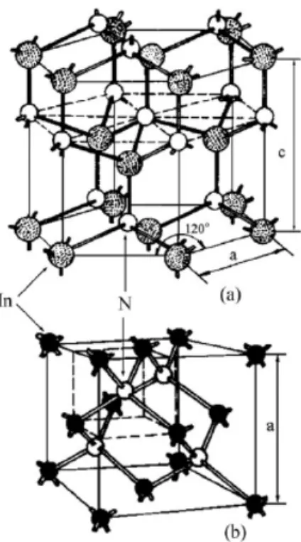
In analogy to most other compounded semiconductor materials, the nitrides have tetrahedrally coordinated atomic arrangements, resulting in either cubic (zincblende) or hexagonal (wurtzite) lattice structures[11]. Among them, the wurtzite crystalline structure is commonly observed for MOCVD and MBE growth nitride semiconductors which always give better results in term of electrical and optical properties. Up-to-date, the physical and chemical properties regarding nitride materials have been mainly focused on GaN, AlN, and InGaN ternary alloys, rather few results on InN. Generally speaking, the epitaxial InN film grown on sapphire is found to be hexagonal wurtzite, so is our MOCVD grown InN nanodots.
Wurtzite InN has four atoms per unit cell, where zincblende InN has two atoms per unit cell. For these two structures, In atom is involved in a tetrahedron of N atoms. And the difference between wurtzite and zincblende InN is its stacking sequence. For wurtzite InN, the stacking sequence is along the [0001] direction, while it is along the [111] direction for zincblende InN.
2-3 Photoluminescence
The Photoluminescence (PL) was used for measurement of the optical properties of InN dots in this thesis. PL is known to be a powerful and non-destructive technique to probe the optical emission properties of materials, especially for luminescent semiconductor. By analyzing the PL spectra, one can identify the impurity types, the band gap energy, and solid composition of semiconductors. However, it is difficult to correlate the PL intensity with concentration of the impurity, since the recombination of photocarriers generally involve rather complex non-radiative recombination routes either through deep-levels or surface states. The photoluminescence process typically involves three steps: namely, excitation, thermalization, and recombination. The electron-hole pairs generated by incident light, which relaxed instantly into quasi-thermal equilibrium conditions, will recombine together to produce photons. The luminescence of semiconductors can be attributed primarily to three major optical transitions: namely, the excitonic edge emission, the donor-acceptor pair emission, and deep-level related emission. Besides, the full width at half maximum (FWHM) of the PL peak is also an indication of sample crystalline quality.
I. Band to band transition:
The band to band transition is participated by free electrons and holes between the conduction and valence band. The transition occurs in direct bandgap material with conservation of momentum. The total e-h recombination rate is given by:
( ) ( )
h d h np RR=
∫
ν ν ≈ , (13)Planck’s constant; ν is the frequency of the emitted photon. II. Free to bound transition:
The free to bound transition occurs between impurity and one of the bands with momentum conservation. Transition of this type is close to the fundamental band gap and has been observed in many semiconductors.
III. Donor-acceptor pairs (DAP) recombination:
Transition between donors and acceptors may take place by optical excitation. Electrons and holes are trapped at D+ and A- sites to produce neutral
D0 and A0 centers. In returning to equilibrium, some of the electrons on the neutral donors will recombine radiatively with holes on the neutral acceptors. It can be represented by the reaction.
D0+ A0→hν+ D++ A-, (14)
The energy of a photon emitted from such transition would be written as:
(
)
DA 2 A D g DA R Q E E E h E ε ν = − + + = , (15)where ED and EA are the binding energies of donor and acceptor, respectively.
Q is the elementary charge, ε is the dielectric constant of the material, and RDA
is the effective donor acceptor separation. IV. Non radiative transition:
Several possible mechanisms lead to non-radiative transitions. And non-radiative recombination will affect the luminescence efficiency.
(i) Generation of phonons due to vibrations.
(ii) All defect site may not act as recombination centers to allow the carriers to recombine radiatively.
(iii) Auger process, in which the energy lost by the capture carrier excites another nearby carrier in the crystal. It gives rise to energy loss
non-radiatively. The other carrier can return to a lower energy state by multiple phonon emission.
Chapter 3 Experiments
Because of low effective mass (0.1m0 for electron and 1.67m0 for hole),
high electron mobility (4400 cm2 V-1 S-1 at 300K) and high peak velocity (4.7×107 cm/s), InN has displayed itself a very promising semiconductor in the applications of high-speed and high-frequency electronic devices[3,12]. More recent studies in InN show its bandgap to be about 0.69 eV, rather than the previously reported 1.9 eV, resulting in a large k⋅p interaction and strong nonparabolic conduction[5,6]. This unexpected discovery opens a wide opportunities for InN in the fabrications of optoelectronic devices, since its ternary and quaternary alloys with GaN and AlN can extend the emission bangap from 6.2 to 0.69 eV, covering the spectra not only the entire visible region, but also ultra-violet and infrared areas. Besides, possibly due to strong interaction between the conduction band and the light hole valence band, the measured InN PL peak energy exhibits almost no shift as the measured temperature changed from 10 to 300K. Such a characteristic would benefit to fabricating 1.3 to 1.55 μm laser diodes with high wavelength-stability, advantageous to optical communications. Although lots of physical properties regarding InN bulk materials have been published, few results are addressed on InN nanodots. Currently, the commonly used growth techniques for InN growth are molecular beam epitaxy (MBE) and metalorganic chemical vapor deposition (MOCVD) techniques. Because of the low growth temperature, the InN nanodots grown by MBE exhibit rather noisy signals in photoluminescence measurements. As for MOCVD, the optical properties of the InN dots were first reported by Ruffenach et al. prepared by conventional method. By capping with SiO2, which suppressing the surface states, and hence the non-radiative
recombination, they find a strong blue shift in emission energy from the quantized effect[7]. The systematic study of quantization of energy as a function of dot size was lately demonstrated by W.C. Ke et al. using a modified MOCVD growth method, flow-rate modulation epitaxy (FME), in which the source precursors were introduced into reactor alternatively[13]. By using GaN as the capping layer, the emission energy of these InN dots is shifted continuously from 0.78 to 1.07 eV as the average dot height is reduced from 32.4 to 6.5 nm.
It has been suggested that the heteroepitaxy growth of InN on GaN (0001), in which the lattice mismatch is 10.2%. However, systematic studies of the InN islands size distribution and island shape and aspect ratio, which are important to understand the evolution of 3D islands grown in the SK or VW modes, are still rare. In this study, we focus our study by using conventional MOCVD to investigate the dot evolution of InN islands at its infant age, regarding the dot morphology, size as well as density as a function of growth coverage.
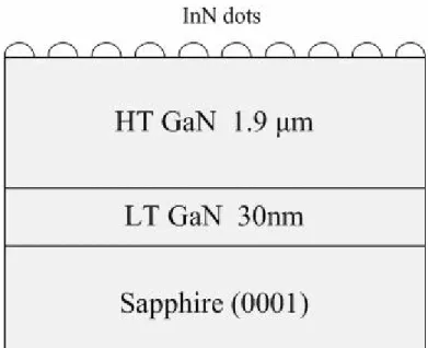
3.1 Sample preparation
The self-assembled InN dot samples were grown on (0001) sapphire substrate by conventional metalorganic chemical vapor deposition growth method using an Aixtron 200/4 horizontal quartz glass reactor at 200 mbar. The substrate temperature is measured by inserting the R-type thermcouple into a susceptor, which has a deviation of approximately ±2℃. In this study,
trimethylgallium (TMGa), thermostated at 5℃, trimethylindium (TMIn),
thermostated at 17℃, and liquid ammonia (NH3) are source precursors for Ga, In
and N elements, respectively. The corresponding equilibrium vapor pressures of Ga and In are 182.3 and 1.73 mmHg. Prior to the epilayer growth, the sapphire substrate was annealed at 1150℃ for 10 minutes in a H2 ambient to remove any
residual impurities on the surface The temperature was then lowered to 510℃ to
commence 30 nm-thick GaN nucleation layer at molar flow rates of 2, and 1600scm for TMGa and NH3, respectively, followed by high-temperature (1130
℃) 1.9 μm-thick GaN buffer layer growth at flow rates of 50, and 2700 sccm for
TMIn and NH3, respectively. The InN dots were subsequently grown at
650℃with a V/III ration of 30,000 and a growth rate of 2ML/min.The corresponding TMIn flow rate was 50 sccm, and NH3 flow rate was 2700, High-purity hydron (dew point < 110℃), purified by Johnson Matthey purifier,
was used as carrier gas for deposition of nitride crystals except for InN dot growth, where nitrogen gas was employed in order to suppress the nitrogen reevaporation from InN film. The growth rate, defined as the ratio of the total volume of InN to the growth time, was measured by atomic force microscopy. To investigate the evolution of InN dots on GaN, a series of samples were performed with a deposition time varied from 22s, 30s, 37s, 45s, 1min, 1.5min,
2min, 3min, 4min, to 6min. We did not consider about the influence of kinetic effects, such as growth rate and temperature. After the growth InN, the NH3 flux
of 4000sccm was continuously flushed while the susceptor was cooling down to room temperature. The structure of the deposition is shown in figure 3-1. Detailed growth conditions are given in Table 3-1.
Fig. 3-1-1. Scheme of deposition InN on GaN buffer
Table 3-1: The details of InN dot growth conditions.
Time (min) Tempe rature (℃) Pressure (mbar) NH3 (mol/min) TMGa (mol/min) TMIn (mol/min) Thermal cleaning Nucleation Recrystallization GaN buffer layer InN nanodots 10 8 3 60 1150 510 1130 1130 650 500 100 400 200 200 - 7.14×10⁻² 1.34×10⁻¹ 1.12×10⁻¹ 1.21×10⁻¹ - 1.18×10⁻⁵ - 5.89×10⁻⁵ - - - - 3.99×10⁻⁶
3.2 Atomic force microscopy (AFM)
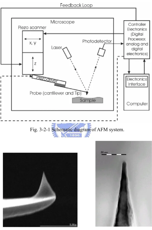
In early of 1980s, Binning and Rohrere (IBM lab) invented the tunneling electron microscopy which can measure the conductor material surface characteristic. But the measurement is just for conductor materials for tunneling electron microscopy. Since that, in 1986 the IBM troup further invented atomic force microscopy, which is one of the foremost tools for imaging, measuring and manipulating matter at the nanoscale.
The configuration of AFM system is shown in Fig.3-2-1. The tip is on the cantilever is controlled by AC and DC voltages. The cantilever will have maximum amplitude for the AC signal at the resonance frequency. As the scanning process, the tip will affect the amplitude of cantilever. Utilizing the reflective optical signal from the tip, we may analyse the surface morphology of sample. There are three modes of scanning for the AFM system.
(I) Contact mode:
In this mode, the tip touches the surface to scan over the sample surface. The piezoelectric scanner enforces the tip with a constant force as the electrical feedback loop. If the height is changing, the system will detect the reflection signal to modulate the height of cantilever to keep the constant force. The height of cantilever will thus provide the surface morphology. Resolution in height is 0.1 nm and diameter is 10 nm.
(II) Non-contact mode
In order to avoid destroying the sample during scanning, non-contact mode is frequently being used. Using long range Van der Waale’s force between tip and sample surface, it vibrates with smaller amplitude. Although the non-destroying of non contact mode, it is not sensitive to detect the changes of
height, the resolution is only about 50nm in height under the environment of atmosphere.
(III) semi-contact mode
The semi-contact mode is modified from the non-contact mode, the amplitude of the cantilever is enlarged, and the height between the tip and the sample is reduced. The resolution of semi-contact mode is higher than non-contact mode. This mode is also applicable to characterize the surface distribution of the magnetic and electric field, elasticity and viscosity. Resolution in height is 0.1 nm and diameter is 7 nm.
Scanning probe microscopy (SPM) system used in our lab is Slover P47H, manufactured by the “Molecular Devices and Tools for Nano Techology (NT-MDT)” in Russia. It can be operated for morphology measurements, EFM (scanning electric force microscopy), and SKM (scanning Kelvin probe microscopy), etc. In our studies, the InN dots morphology was measured by semi-contact mode in order to optimize the resolution and avoid probe destruction. The AFM probe, which has a cantilever about 50 or 80 μm and a sharp tip with a radius of curvature about 10 nm (Fig. 3-2-2), is also from NT-MDT.
Fig. 3-2-1 Schematic diagram of AFM system.
3.3 Photoluminescence (PL)
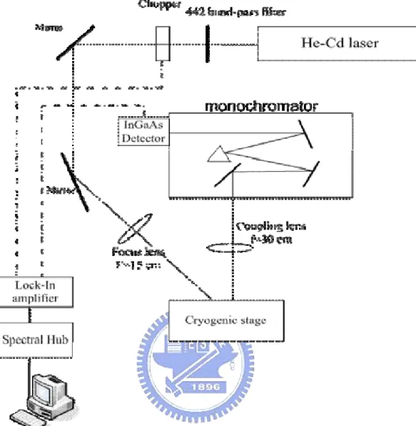
The micro-PL consists with optical microscopy system (Olympus BH2) as shown in 3-3-1. A He-Cd laser (KIMMONIK5552R-F), of wavelength 442nm and power density of 35mW/m2, is used as the excitation laser in our experiment. Laser beam passes through a 442nm band-pass filter to filter out the plasma line. Using reflection mirror to guide laser through beam splitter and objective lens (f=15cm) to focus on sample. The luminescence signals were collected by another lens (f=30cm) and coupled into the monochrometer (ARC Pro 500). The dispersed signals were detected by the EOS extended InGaAs detector, and processed using lock-in amplifier and Acton Spectra Hub. To increase the signal to noise (S/N) ratio. The amplified signals were sent to a computer for data processing and analyzing.
Low temperature micro-PL was carried out by using a closed cycle cryogenic system (APD HC-2D). The temperature was varried from 13 to 300K by Ladeshore 330 temperature controller.
Chapter 4 Results and discussion
4.1 Critical thickness
The growth mode of InN is of fundamental interests for growing high quality InN material, particularly on GaN buffer layer. The lattice constant of axis of InN is 5.718Å and GaN is 5.189Å[29]. The corresponding lattice mismatch between InN and GaN is
% . . . . a a a GaN GaN InN 102 189 5 189 5 718 5 − = = − (1)
By referring the equilibrium model proposed by Daruda et al., we learn that such a lattice mismatch is at the ambiguity value, which is close to the theoretical transition boundary between the VW and SK mode, 10%. That is the InN on GaN growth may undergoes either via SK if the lattice-mismatch is <10% or via VW growth modes for the rest of mismatched values. Ng et al. have observed that InN on GaN island growth using molecular beam epitaxy at 450℃ exhibits both 2D layer-by-layer and 3D features. Their results indicate the growth mode of InN islands on GaN seems dependent greatly on growth conditions: low temperature and/or high N flux (relative to In) favor SK mode growth, whereas high temperature and high In flux tend to lead to a 2D growth feature. The occurrence of 2D precursor islands, i.e. wetting layer, prior to the genuine 2D-3D transition has also been observed in the InAs/(Al,Ga)As and GaN/AlN system, where the lattice mismatch are 7 and 4%, respectively, resembling the characteristics of a typical SK growth manner. Nevertheless, our preliminary results suggest that the VW growth, rather than SK mode, governs our InN-on-GaN island growth at a growth temperature of 650oC, at least at conditions when metalorganic vapor phase epitaxy growth method is
a
ε employed.
Normally, the VW growth mode of heteroepitaxy occurs if the surface free energy of the substrate (σsubstrate) is less than the sum of the surface free
energy of the deposition film (σfilm) and the interface strain energy (σinterface).
On the other hand, if the film strain energy of wetting layer is required to surface free energy of the substrate is greater than the sum of the surface free energy of deposited film and the interface strain energy Even if the the substrate free energy is larger than the sum of the surface free energy of deposition film and interface strain energy, as long as the wetting layer is less than 1ML, the 3D growth is also categorized as the VW island growth mode .On the other hand, if film strain energy of wetting layer is n For the case of InN grown on GaN, the surface free energy of GaN is 124.92meV, considerably larger than the sum of the surface free energy of the deposition InN σInN, 77.29meV, and the interface strain energy σinterface, 47.63,
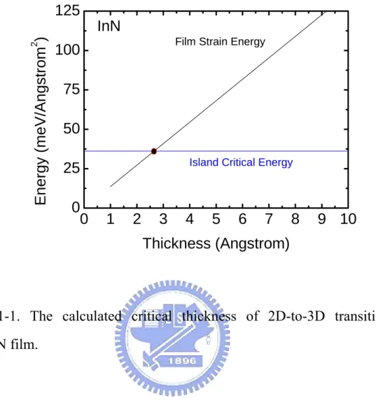
unfavorable to the sustaining the continuous layer-by-layer 2D growth feature. In this situation, we need to consider about the strain energy and the SK mode might become govern. The SK mode of growth, the 2D to 3D transition will happen as Θ + + < 2 int ( ) 2 1 a erface InN GaN σ σ Y ε σ , (2)
where Y is the Young modulus (1.24x10⁴ GPa), is in plan strain ( GaN GaN InN a a
a − ), and Θ is the thickness of InN wetting layer. Using this formula, we can find the critical thickness of InN grown on GaN is 0.92ML (0.263nm), less than 1 ML. As shown in Fig. 4-1-1, the blue line is the island critical energy which is defined asσ – (σ +σ ), and the black line is film
strain energy which is defined as ( )2
2 1
a
Y ε . The intersection point of these two
lines is the critical thickness.
Since the critical thickness of required wetting layer is less than 1ML, the theoretical prediction infers a VW growth mode predominating the InN island growth on GaN substrate.
0 1 2 3 4 5 6 7 8 9 10 0 25 50 75 100 125
Island Critical Energy
Film Strain Energy
InN Energy (m eV/ A ngs tr om 2 ) Thickness (Angstrom)
Fig. 4-1-1. The calculated critical thickness of 2D-to-3D transition for InN/GaN film.
4.2 Surface morphology of InN dots
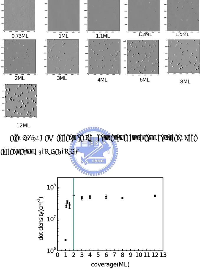
The morphological properties of InN dots on GaN were investigated by atomic force microscopy (AFM). Fig. 4-2-1 shows 10×10 μm2 AFM images of InN/GaN samples with InN coverage ranging from 0.73 ML to 12ML. The surface morphology and associated dot density as a function of coverage are depicted in Fig. 4-2-1 and 4-2-2, respectively. Virtually no dot growth was observed at coverage of 0.73 ML and few InN dots with density as low as 2.2×106 cm-2 start to form on the surface as the coverage exceeds 1 ML. It is interesting to note that once the dots are formed, the dot density begins to increase sharply with the increasing coverage and finally saturate at a value of ~5×107 cm-2 when the InN coverage is beyond 2 ML. The saturated dot density is considerably lower than those reported by other MOVPE groups grown at temperatures of 500-600℃, ~108cm-2, as a consequence of high migration length of adsorbed atoms due to the high growth temperature of 650℃ used here.
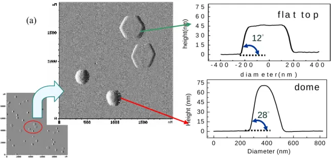
In addition, we also found a bimodal growth feature in our InN/GaN dot growth, where two types of dots, namely, flat-top and dome islands, with different surface morphology, height, diameter as well as aspect ratio, defined as the ratio of dot height to diameter, contact angle, form concurrently on the surface of film, irrespective of growth coverage. For the flat-top island, the base of the dot is of hexagonal shape with a large flat plateau on top of the island. The other type is dome-shaped island. The corresponding contact angles are 12o and 28o for flat-top and dome-shape, respectively. The base of this kind of island is smaller than flat-top island and exhibit blurred hexagon. For example, for 4 ML sample, where the dot saturation occurs, the diameter of dome is ~325 nm, whereas that of flat top is ~450 nm. Comparing the height
of these two types of dots, we can find that the average height of dome-shaped island, 9.44 to 89.87 nm, is higher than that of flat-top, 3.36 to 30.00nm. The corresponding aspect ratios, defined as ratio of height to diameter are ~ 0.02-0.04 and 0.06-0.2 for flat-top and dome-shaped islands, respectively. Such a bimodal distribution has also been observed in the InAs/(Al,Ga)As, GaN/AlN, Ge/Si system, formed owing to the relaxation of the elastic energy barriers via change in shape and a maximum permissible size for dots without generation of dislocations, resulting in a transition process from pyramid to dome[14,15,16]. However, this may not be the case for our InN on GaN grown by MOVPE, since both types of dots conceivably are dislocated, arising mainly from the extended dislocation originated at interface between the underlying GaN buffer layer and sapphire substrate due to large lattice-mismatch. The issue of the complex growth evolution of dots, especially under far from equilibrium growth conditions for MOCVD, is still an interesting problem of work.
Fig. 4-2-1. AFM images of InN dots grown at various coverage. Each image shows a 10μm×10μm. 0 1 2 3 4 5 6 7 8 9 10 11 12 13 106 107 108 dot density(cm -2 ) coverage(ML) 0 1 2 3 4 5 6 7 8 9 10 11 12 13 106 107 108 dot density(cm -2 ) coverage(ML)
Fig. 4-2-2. Total dot density various coverage.
0.73ML 1ML 1.1ML 1.2ML 1.5ML
2ML 3ML 4ML 6ML
8ML
Fig. 4-2-3. (a)AFM images of two types 3D InN dots grown at 4 ML coverage. Line profiles across (b) flat-top (c) dome shaped islands. Image size is 2μm × 2μm. - 4 0 0 - 2 0 0 0 2 0 0 4 0 0 0 1 5 3 0 4 5 6 0 7 5 he igh t( n m ) d i a m e t e r ( n m ) f l a t t o p 12° 0 200 400 600 800 0 15 30 45 60 75 Heigh t (nm) Diameter (nm) dome 28° (a)
4.3 Bimodal distribution of InN islands on GaN
Statistical distributions of diameters and height for both flat-top and dome-shaped InN islands, denoted by red and green bars, respectively, for various samples grown with different coverage are shown in Fig. 4-3-1. For each sample, regardless of different growth coverage, the measured averaged diameter of flat-top island is in general larger that of dome-shaped island; whereas their heights behave conversely.
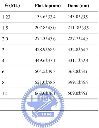
More detailed results concerning the variations of the island diameter as well as height of InN dots against growth coverage are summarized in Fig. 4-3-2 and Fig. 4-3-3. The error bar used here denotes the standard deviations of the associated diameter and height of the as-grown InN dots. As far as the dot diameter is concerned, we can find the diameter tends to increase monotonously from 133nm to 428 for flat-top island and 143 to 332nm for dome-shape islands as the InN coverage is increased from 1 to 3ML. Further deposition of InN, however, brings slow increases in their diameters. The corresponding diameters increase gradually from 428nm to 667 and 332 to 509nm for flat-top and dome-shape islands as InN coverage is increased from 3 to 12ML.
It should be noted that the formation of the islands commence at a InN coverage close to ~1 ML. Preliminary results show both types of InN islands are generated simulataneously at the initial stage, unlike the case of Ge islands on Si substrate, where only pyramid-shaped Ge islands are appeared initially and dome-shaped islands occur lately under a situation when the dot volume of growing island exceeding a critical value, which is typically ~9000 nm3 for Ge/Si system[17].
For commonly observed Ge islands on Si substrate, the Ge islands form coherently on the substrate. There are two strain related effects responsible for stabilization of island size. One is biased adatom diffusion, which is caused by the accumulation of atoms in the island. That is as the island grows, the strain-induced field develops around the island, causing a decay of strain energy as we move away from the edge of the island. This means that if atoms are depoited near the island, strain biases their otherwise random motion, generating net current of adatoms away from the island. The other is enhanced detachment of atoms from the edge of larger islands. For large islands the strain energy at edge becomes comparable to the bonding energy of edge atom, enhancing its detachment, thus leading to a gradual dissolution of the island. The simultaneous action of above both effects leads to a kinetic mechanism stabilizing the island size: as islands grow, a strain field develops, that helps to dissolute the edge atoms and pushes them away from the islands. As it known, the energy barrier at the edge of island increases with the increasing dot volume. The existence of energy barrier prevents the adatoms from hopping down a step (Ehrlich-Schwoebel barrier), an uphill current will be created, which will lead to high aspect ratio[22]. Since that, the dome-shape may be the evolution results from the flat-top, which has a barrier at the edge and tends to a vertical growth. Unlike the case of coherent island, where the aspect ratio will increase with the increasing coverage because of Ehrlich-Schoebel barrier effect, when island induces or encounters dislocation aspect ratio that corresponds to the minimum free energy in the dislocated system[23]. In general, the higher aspect ratio dots have lower free energy[24]. Furthermore, the newly deposited atoms also diffuse away from the large island. This
nucleation of new islands nearby. For InN dots on GaN, the dots are almost dislocated and the residual strain in the dots depends on the dot size, as more dislocation will be introduced as further growth. The study of J. G. Lozano et al. indicate that InN dots tend to form preferentially right on top of dislocations originating from the interface of underlying GaN buffer layer and sapphire substrate, rendering a reduced energy on the GaN surface[18]. Thus, we believe the have lower energy. It suggests that the growth in diameter from 1 to 3ML is due to dislocation from GaN, which lead to fast lateral growth and a constant height. However, the energy can be relief by dislocations is a finite value, and the further deposition materials will contribute to height growth, which have lower energy comparing with lateral growth.
Fig.4-3-1. Diameter and height distributions for InN islands with coverages
varied from to ML. 0 5 10 15 20 flat-top dome 0 5 10 15 20 0 5 10 15 20 0 5 10 15 20 0 5 10 15 20 100 200 300 400 500 600 700 800 0 5 10 15 20 Diameter 0 5 10 15 20 flat-top dome 0 5 10 15 20 0 5 10 15 20 0 5 10 15 20 0 5 10 15 20 20 40 60 80 100 120 0 5 10 15 20 Height(nm)
0 1 2 3 4 5 6 7 8 9 10 11 12 13 100 200 300 400 500 600 700 diameter(nm) coverage(ML) dome flat top
Fig.4-3-2. Dot diameter against coverage
0 1 2 3 4 5 6 7 8 9 10 11 12 13 0 20 40 60 80 100 dot height(nm) coverage(ML) dome flat top
Table 4-3-1 Summary of diameters of flat-top and dome-shaped InN islands grown with different coverages.
Θ(ML) Flat-top(nm) Dome(nm) 1.23 133.6±33.4 143.0±29.9 1.5 207.8±45.0 211. 8±53.9 2.0 274.3±43.6 227.7±44.5 3 428.9±68.9 332.8±64.2 4 449.6±37.1 331.1±52.4 6 504.5±39.3 368.8±54.6 8 521.0±58.8 399.1±56.5 12 667.0±76.1 509.0±55.6
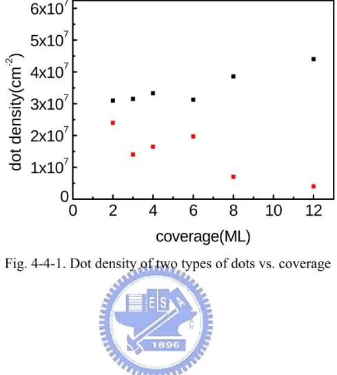
4.4 Vicissitudes of two shapes of InN dots
In Fig.4-4-1, we display the variations of dot densities for flat-top and dome-shaped InN islands only for coverages larger than 2 MLs. As discussed earlier, at this growth coverage region the total dot density remains virtually unchanged. However, we do observe an opposite tendency of variations of dot densites concerning the flat-top and dome-shaped islands. As can be seen in the figure, at a coverage of 2 ML the dot densities of these two dots are about the same, lying at 2.4x10⁷ and 3.1x107cm-3 for flat-top and dome-shaped dots, respectively; as the coverge grows the dot density of dome-shaped island tends to increase, whereas that of flat-top island tends to decrease. One can notice that when the coverage reaches 12 ML, rather few flat-top islands can be found on the surface of sample. The resulted densities of flat-top and dome-shaped islands are 4.0x10⁶ and 4.4x107cm-3, nearly an order of difference in magnitude. The above finding suggests that the formation of dome-shaped islands seem energetically more favorable under the circumstance of high growth coverages.
Bimodal distribution has also been observed in Ge/Si and InAs/GaAs systems. The relevant shape transitions have also been discussed intensively. The illustrative example is Ge/Si system. The shap transitions in Ge/Si have been attributed to either stress relaxation or intermixing between island and substrate. For Ge/Si system, one is pyramidal island, having the characteristics of square-based islands bounded by {105} facets; the other is dome-shaped island with structures with large number of facets that look rounded at lower resolutions[19]. Both of the islands are type of coherent island. For these
3400nm3 for InAs/GaAs, respectively. When the dot volume is small, most of the dots are in the form of so-called pyramid (or hut) shape with facet contact angle to the underlying substrate of 25° and aspect ratio of 0.11[20]. Once the dot volume exceeds the critical volume, these coherent dots begin to transform from low-aspect-ratio pyramidal islands into high-aspect-ratio dome-shaped ones because of the relaxation of large stress in the island. However, different story may occur for shape transition in InN/GaN dot system. The primary difference between InN/GaN system and InAs/GaAs or Ge/Si is that the InN dots are more likely dislocated whereas they are coherent for InAs/GaAs or Ge/Si[21].
As mentioned earlier, for InN island growth on GaN the dome-shaped island becomes predominant as the growth coverage beyond 8ML. Because of high island volume associated with both types of islands, ~40,000-8,700,000 nm3, approximately 100 times higher than the critical volume of coherent islands that observed in either Ge/Si and InAs/GaAs material system, it is considered that both of the bimodal islands in InN/GaN are highly dislocated. This is ascribed to the characteristic of high density of dislocation density, ~109-1010cm-3, of GaN template employed for our InN dot growth, stemming from the heteroepitaxial growth of GaN on highly lattice-mismatched sapphire substrate (12% mismatch). Consequently, there exhibits one dislocation on the surface of GaN buffer layer for every 100-300 nm in distance. Since the base diameters of our InN islands are around 274 and 227 nm for flat-top and dome, respectively, supportive of containing dislocation for most InN islands in our samples. This reason accounts well for the hypothesis of dislocated InN islands here. The above argument is in good agreement with recent observation by J. G.
with GaN pure edge threading dislocations (TDs), which act as nucleation site for InN island growth[18].
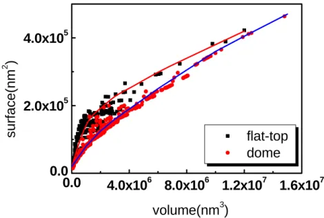
Fig. 4-4-3 shows surface-volume plot for both types of flat-top and dome-shaped InN islands, which is an energetically relevant measure of size and shape. For the cases in InAs/ GaAs or Ge/Si system, the scatter plot reveals two distinct shapes, which has its own slope of surface to volume value [18]. However, we observed quite different results in InN islands /GaN system. The corresponding surface-to-volume plots in InN varies almost continuously for both types of dome-shaped and flat-top InN islands. Comparing high coverage region, steeper slopes are attained at low coverages. Generally, the mean slopes of dome-shaped islands are higher than that of flat-top ones throughout the entire volume region. It is worth to mention that at low volume region, the slop of flat-top is deceased continuously with the increasing growth coverage and moves gradually toward the values close to that of dome-shaped islands. At volumes higher than ~3x10⁶ nm3, the slopes of the flat-top islands appear to have values almost the same as that of dome-shaped islands, which seems to imply that flat-top island changes its shape with the increasing island volume and finally transform itself into a shape of dome-shaped ones. The above phenomenon explains why the density of dome-shaped island is increased with the coverage, accompanied simultaneously with the decreasing of the density of flat-top island, while total density of InN islands can still maintain about the same for growth coverages > 2ML. From energy point of view, the change of growing facets on the island leads to changes of surface energy and island volume which can result in the shape transition of island. Exemplary result is Ge islands on Si. For this case, it has shown that the hut is
volume shape transition occurs which make hut transform into dome-shaped island. Nevertheless, the critical volume provides a necessary but not sufficient condition for shape transition. Since the shape transition is a first-order transition, there appears an energy barrier to trap the island in a matastable configuration.
The above finding is further confirmed by the contact angle-coverage plot, shown in Fig. 4-4-2. In this figure, the contact angles of entire InN islands also distribute bimodally at low coverages. The lower contact angle ~7o, corresponds to the type of flat-top island and higher contact angle ~21o, dome-shaped one. At 2 ML, the mean contact angles are ~7o and 21o for flat-top and dome-shaped islands, respectively. The contact angles shift monotonously towards ~10o and ~28o when the coverage reaches 4 ML. At 6 ML, an additional peak ~20o, appears, a value virtually the same as the mean contact angle of dome-shaped islands at 2 ML. The plane view of AFM image and line profile are shown in Fig. 4-4-4. As the coverage higher than 6ML, it is found that the count of mean contact angle (11o) for flat top drop considerably. Its intensity becomes about 10 times lower than that of dome-shaped islands and reaches approximately zero for coverages exceeding 8 ML. Concerning the evolutions of contact angles for the other two existed structures, we can found the mean contact angle of domes-shaped stablizes at ~35o for coverages beyond 6 ML and at the same time the contact angle of newly developed island, which we believed is the type of flat-top islands, moves gradually toward to higher angles ~22o, similar to the case of evolution of dome-shaped islands at low coverages and finally completely merged into main stream of distribution of contact angles of dome-shaped islands at 12 ML. The contact angles of
respectively. Normally, the chemical potential of an island decreases continuously with growing size, due to the smaller surface/volume ratio. Assuming that the surface energy is the same for every allowed facet, the island energy is described as[27]
-Vα α V
E= 2/3 4/3 , (3)
The chemical potential per volume can be written as
-α V α μ 4/3 -1/3 3 2 = , (4)
From the simulation, the higher aspect ratio will have lower energy with larger dot volume. As a result, material diffuses from smaller to larger islands via either coarsening, Ostwald ripening, or shape transition process. For coarsening or Ostwald ripening, some island continue to grow while others shrink and disappear. For a given volume, its equilibrium shape of island, for sure, has a lowest free energy. The flat-dome islands, which have the contact angle of ~20o, almost have the same volume of dome-shape ones with contact angle ~35o at each coverage. The scatter plot of contact angle of InN dots as a function of their volume is shown in Fig. 4-4-5. The contact angles of both types of dots increase with volumes, and the contact angles of dome-shape saturate around ~35o at volume of ~3x10⁶nm3. The contact angles of flat-top shown in Fig.4-4-2 grow from 70 to 35o which is identified as dome shape which is respect in the dot density of flat-top decrease with coverage. Since the energy of island will have lower energy in high aspect ratio over the critical volume, the dome-shape of dots will tends to from at large volume. We deduce that there is a shape transition between flat-dome and dome-shape, which have the same volume, for example ~3.3x10⁶nm3 for flat-dome and 3.2x10⁶nm3 for dome at 6ML, but reducing the island base area and increasing the height. The
existence of one additional contact angle at 6 ML, together with a clear transition of slope of surface-to-volume plot at a volume of ~ 3x10⁶nm3 and fact of fast vanishing in dot density of flat-top island suggests that the flat-top islands are hardly to sustained themselves at volumes greater than ~3x10⁶ nm3, indicating of energy in favor of dome-shaped island at this high volume region.
0
2
4
6
8
10
12
0
1x10
72x10
73x10
74x10
75x10
76x10
7dot
density
(c
m
-2)
coverage(ML)
0 8 16 24 32 40 8ML 0 10 20 30 40 50 60 0 8 16 24 32 40 contact angle(degrees) 12ML 0 8 16 24 32 40 4ML 0 8 16 24 32 40 6ML 0 8 16 24 32 40 2ML 0 8 16 24 32 40 3ML
0.0 4.0x10⁶ 8.0x10⁶ 1.2x10⁷ 1.6x10⁷ 0.0 2.0x10⁵ 4.0x10⁵ flat-top dome surface(nm 2 ) volume(nm3)
Fig. 4-4-3. Scatter plots with different coverage.
20o 11o 35o -300 -150 0 150 300 0 20 40 60 80 100 120 Dot h e ig ht(n m) Diameter(nm) dome -300 -150 0 150 300 0 20 40 60 80 100 120 Dot h e ig ht(n m) Diameter(nm) flat-top -300 -150 0 150 300 0 20 40 60 80 100 120 Dot h e ig ht(n m) Diameter(nm) flat-dome 20o 11o 35o 20o 11o 35o -300 -150 0 150 300 0 20 40 60 80 100 120 Dot h e ig ht(n m) Diameter(nm) dome -300 -150 0 150 300 0 20 40 60 80 100 120 Dot h e ig ht(n m) Diameter(nm) flat-top -300 -150 0 150 300 0 20 40 60 80 100 120 Dot h e ig ht(n m) Diameter(nm) flat-dome
0.0 4.0x10⁶ 8.0x10⁶ 1.2x10⁷ 0 10 20 30 40 50 contact angle(degree) Volume(nm3)
Table 4-4-1 Dot density of flat top and dome shapes
Flat top dome total
1.1ML 1.1×10⁷ 1.54×10⁷ 2.64×10⁷ 1.23ML 2.05×10⁷ 1.4×10⁷ 3.45×10⁷ 1.5ML 1.15×10⁷ 1.65×10⁷ 2.80×10⁷ 2ML 2.40×10⁷ 3.10×10⁷ 5.50×10⁷ 3ML 1.40×10⁷ 3.15×10⁷ 4.55×10⁷ 4ML 1.65×10⁷ 3.33×10⁷ 4.98×10⁷ 6ML 1.97×10⁷ 3.13×10⁷ 5.09×10⁷ 8ML 7.00×10⁶ 3.86×10⁷ 4.56×10⁷ 12ML 4.00×10⁶ 4.40×10⁷ 4.80×10⁷
4.5 PL results
For light-emitting devices, the size of low-band-gap quantum dots embedded in the active layer is a matter related to the device luminescence efficiency. The use of a smaller dot structure will certainly result in a better carrier confinement, and quantum effects to improve the quantum efficiency. In this section, we carried out photoluminescence measurements at 13K to investigate the optical properties of our MOVPE-grown InN dot samples with different coverages. The results are shown in Fig. 4-5-1.
As can be seen in the figure, the PL intensity is, as expected, increased with the increasing coverage and no signal can be detected for samples grown with coverages lower than 2 ML due to the detection limit of our PL system. One can notice that for 2, 3, 4, 6ML samples there are two peaks located at ~0.73eV and 0.77eV in the PL spectra, which is contributed to deep acceptor and near band edge transition, respectively. As the coverage is increased to 10 and 12ML, the higher energy peak eventually predominates the spectra. The resulted FWHM is found to decrease from 99 to 60 meV as the growth coverage is increased from 3ML to 12ML, respectively. It is interesting to note that for those InN dot samples with coverage <6ML, whose mean dot heights are less than 35 nm, blueshifts in PL peak energies should be observed because of quantum size effects. For example, a blueshift of 270meV has been observed for capped InN QD ensemble of mean height of 6.2nm. Nonetheless, no apparent peak shift is observed. Since all of our InN dot samples studied here are uncapped, the nearly invariance of PL peak energy is considered highly probably related to the accumulation of large number of surface electrons in our InN islands, owing to extraordinary high density of surface
states existed inherently to this type of film. Under this circumstance, the surface electrons which spreading spatially separated will lower the transition energy to counterbalance the blueshift of energy caused by quantum size effect.
0.5 0.6 0.7 0.8 0.9 1.0 1.1 1.2 0.00 1.50x10⁵ 3.00x10⁵ 4.50x10⁵ 6.00x10⁵ In tensity(a.u.) Energy(eV) 3ML 4ML 6ML 8ML 12ML
Fig. 4-5-1. PL spectra of InN dot vs. coverage ML low energy High energy
3 0.731 0.778
4 0.729 0.778
6 0.729 0.773
8 0.728 0.761
Chapter 5 Conclusions
We have studied the evolution of InN islands on GaN grown by MOVPE at 650oC in terms of morphological shape, height, diameter, aspect ratio, emission peak energy and it’s FWHM. Experimental results indicate that bimodal growth feature was taking place in our InN island/GaN system. There are two types of InN nanodots, assigned as flat-top and dome-shaped islands, exhibit characteristics of the hexagonal shape base with a flat plateau on top and a circular base with a dome on top.
It is found that the diameters of our InN islands tend to increase sharply from 133 to 428 nm for flat-top island and 143 to 332 nm for dome-shaped island for 1 to 3 ML coverage at a lateral growth rate of ~100 nm/ML. Then, the growth became slow from 428 to 667 nm and 332 to 509 nm in the range of 3-12 ML at a growth rate of ~20 nm/ML, which is nearly 5 times slower in growth for two coverage regions. Such a faster lateral growth rate at lower coverages is considered to relate with the characteristics of InN nanodots grown on the top of dislocation, extending from the interface between GaN buffer layer and sapphire substrate. The reduction of the total energy of island makes the lateral growth more favorably at initial growth stage. However, once the critical volume, is reached, at ~3ML, energy barrier starts building up around the edge of islands. It impedes not only the further attachment of surface adatoms to the edge of island but also directs the island growth to grow preferentially in the vertical direction, causing more and more flat-top islands to transform into dome-shaped islands. As a consequence, at 12 ML nearly all of the InN islands become dome-shaped islands, their respective densities are 4.4 x10⁷ and 4.0x106cm-3.
The transformation of flat-top InN islands into dome-shaped ones can also be revealed by its surface-to-volume plot. The slope of flat-top is found to decrease continuously with the increasing growth coverage and moves gradually toward the values close to that of dome-shaped islands and finally reaches a value almost the same as that of dome-shaped islands as the island volume >~3x10⁶ nm3.
More clear evidence regarding the shape transition can be observed in the plot of contact angle as a function of coverage.
At the beginning, there
exhibits two groups of contact angles peaked at 7
oand 21
o,
corresponding to flat-top and dome-shaped islands, respectively. The
mean peak values of dome-shape islands tend to move gradually
toward higher values with the increase of coverage and finally
stabilize at ~11
oand ~35
o. It is interesting to note that at coverage of 6
MLs one additional group appears at ~21
owhich turns to increase with
its contact angle with increasing coverage and seems to merge
completely into group of dome-shape islands at higher coverages.
Since the island having higher contact angle possesses lower
formation energy, we believe the additional group comes highly
probably from flat-top islands. The plot of surface-to-volume ratio
further confirms the argument of shape transition of flat-top to
dome-shaped island at higher island volume.
Similar to the case ofevolution of dome-shaped island mentioned previously, the contact angles of these islands shift gradually toward to higher values and merge completely into main stream of dome-shaped islands at 12 ML.
In summary, we have investigated comprehensively the evolution of structural parameters of bimodal InN islands. The existence of one additional contact angle at 6 ML, together with a clear transition of slope of surface-to-volume plot at a volume of ~ 3x10⁶nm3 and the fact of fast vanishing in dot density of flat-top islands all suggest that the flat-top islands hardly to sustain themselves at volumes greater than 3x10⁶ nm3. Eventually all InN islands are transformed into dome-shaped island, indicating that dome-shaped island is energetically favored at this high volume and hence high coverage region.
Reference:
[1] S. Nakamura, M. Senoh, and T. Mudai, Jpn. J. Appl. Phys., Part 2 32, L8 (1993).
[2] S. Nakamura, M. senoh, S. Nagahama, N. Iwasa, T. Yamada, T. Matsushita, H. Kiuoku, and Y. Sugimoto, Jpn. J. Appl. Phys., Part 2
35, L74 (1996).
[3] V. W. L. Chin, T. L. Tansley, and T. S. Osotchan, J. Appl. Phys. 75, 7365 (1994).
[4] A. Yamamoto, M. Tsujino, M. Ohkubo, and A. Hashimoto, Sol.
Energy Mater: Sol. Cells 35, 53 (1994).
[5] V. Yu. Davydov, A. A. Klochikhin, R. P. Seisyan, V. V. Emtsev, S. V. Ivanov, F. Bechstedt, J. Furthmuller, H. Harima, A. V. Mudryi, J. Aderhold, O. Semchinova, and J. Graul, Phys. Stat. Solidi(b), 229(3), R1 (2002).
[6] J. Wu, W. Walukiewicz, K. M.Yu, J. W. Ager, E. E. Haller, H. Lu, W. J. Schaff, Y. Saito, and Y. Nanishi, Appl. Phys. Lett. 80, 3967 (2002). [7] R. Intartaglia, B. Maleyre, S. Ruffenach, O. Briot, T. Taliercio, and B.
Gil, Appl. Phys. Lett. 86, 142104 (2005).
[8] W. C. Ke, C. P. Fu, C. Y. Chen, L. Lee, C. S. Ku, W. C. Chou, W. H. Chang, M. C. Lee, and W. K. chen, Appl. Phys. Lett. 88, 191913 (2006).
[9] W.C. Ke, H.Y. Huang, C.S.Ku, K.H. Yen, L. Lww, W.K. Chen,W.C. Chou, M.C.Lee, W.H.Chen, W.J. Lin, Y.C. Chen, and Y.T.Cherng,
Jpn. J. Appl. Phys., 43, L780 (2004).
[11] Z. G. Qian, W. Z. Shen, H. Ogawa, and Q. X. Guo, J.Phys.: Condens.
Matter ,16, R381(2004).
[12] V. W. L. Chin, T. L. Tansley, and T. Osotchan, J. Appl. Phys. 75, 7365(1994).
[13] W. C. Ke, L. Lee, C. Y. Chen, W. C. Tsai, W.-H. Chang, W. C. Chou, M. C. Lee, and W. K. Chen,Appl. Phys. Lett. 89, 263117 (2006).
[14] B. Bansal, M. R. Gokhale, A.Bhattacharya, and B. M. Arora, J. Appl.
Phys. 101, 094303(2007).
[15] C. Adlmann, B. Daudin, R. A. Oliver, G. A. D. Briggs, and R. E. Rudd, Phys. Rev. B, 70, 125427(2004).
[16] T. I. Kamins, G. M. Ribeiro, D. A. A. Ohlberg, and R. S. Williams,
J. Appl. Phys., 85, 2933 (1999).
[17] G. M. Ribeiro, A. M. Bratkovski, T. I. Kamins, D. A.A. Ohlberg, R. S. Williams, Science, 279, 353.
[18] J. G. Lozano. A. M. Sanchez, R. Garcia, and D. Gonzalez, D. Araujo, S. Ruffenach, and O. Briot, Appl. Phys. Lett. 87, 263104 (2005). [19] G. M. Ribeiro, T. I. Kamins, D. A. A. ohlberg, and R. S. Williams,
Phys. Rev. B, 58, 3533(1998).
[20] Y. Zhang, and J. Drucker, J. Appl. Phys., 93, 9583 (2003).
[21] T. KEHAGIAS, A. Delimitis, P. Komninou, E. Iliopoulos, E. Dimakis, A. Georgakilas, and G. Nouet, Appl. Phys. Lett. 86, 151905 (2005). [22] A. L. Barabasi, Appl. Phys. Lett. 70, 2565 (1997).
[23] H. T. Johnson, and L. B. Freund, J. Appl. Phys., 81, 6081(1997). [24] M. Hammar, F. K. LeGoues, J. Tersoff, M. C. Reuter, R. M. Tromp,