國立交通大學
光電工程學系 顯示科技研究所
碩士論文
五環素有機薄膜電晶體之可靠度分析
The DC/AC Reliability of
Pentacene-based OTFT
研究生: 潘皇維
中華民國 九十六 年 七 月
五環素有機薄膜電晶體之可靠度分析
The DC/AC Reliability of Pentacene-based OTFT
研 究 生:潘皇維 Student:Huang-Wei Pan
指導教授:冉曉雯 博士 Advisor:Dr. Hsiao-Wen Zan
國 立 交 通 大 學
光電工程學系 顯示科技研究所
碩 士 論 文
A Thesis
Submitted to Department of Photonics & Institute of Electro-Optical Engineering College of Electrical Engineering and Computer Science
National Chiao Tung University in partial Fulfillment of the Requirements
for the Degree of Master
in
Electro-Optical Engineering July 2007
Hsinchu, Taiwan, Republic of China
五環素有機薄膜電晶體之可靠度分析
研究生:潘 皇 維 指導教授:冉 曉 雯 教授
國立交通大學
顯示工程研究所碩士班
摘要
有機薄膜電晶體,因其具有低溫製程、低成本和製程簡單的優勢,所以有很 好的潛力應用在如可撓曲式面板、感測器和RFID及其他的電子元件。近來的文 獻及研究著重在DC gate bias stress without drain bias,而對於電子元件實際操 作上, drain bias 及操作AC signal的研究比較缺乏。因此此論文將對於DC gate bias with drain bias stress 及AC bias stress做深入的研究。首先,在DC gate bias stress without drain bias部分,ΔVth 隨著時間的關
係,符合Stretched-exponential equation,與現有的文獻一樣的結果。而當Drain bias施加後,ΔVth 會隨VD增加而減小,我們分析得到當VD增加時,通道內載子
濃度的減少,由於載子濃度與ΔVth 成正比的關係,造成ΔVth 的變小。因此我們對
載子濃度歸ㄧ化後可得DC gate bias stress with drain bias中ΔVth 隨時間的關係
亦符合Stretched-exponential equation。
在AC stress部分,在同樣的duty ratio下ΔVth 會隨著頻率越高ΔVth 越小,我
們分析發現pentacene本身的電容與電阻以及與金屬間的接觸電阻所等效的RC 電路,造成通道內載子濃度因RC delay time隨著pulse width的變小而減少,使 得ΔVth 變小。同DC bias stress的部份,亦可對載子濃度歸ㄧ化後可得在AC bias
The DC/AC Reliability of pentacene-based OTFT structure
Student: Huang Wei Pan Advisor: Dr. Hsiao Wen Zan
Institute of Dispaly
National Chiao Tung University
Abstract
As organic thin film transistor has lots of advantage of low temperature fabrication、low cost and easy fabrication, it has good potential for application on flexible display、sensor、radio-frequency identification tags and other electronics. Although studies have been made on DC gate bias stress without drain bias, the drain bias and AC bias stress in actual operation of organic electronic device is unknown. So we focus on the study of DC gate bias with drain bias stress and AC bias stress in this thesis.
First, in the DC gate bias stress without drain bias, the dependence of the threshold voltage shift on the stressing time is found to follow a stretched-exponential function. It is the same as the many recent researchs. When the drain bias is applied, the threshold voltage shift will decrease and be suppressed as the drain bias becomes more negative. Since the threshold voltage shift is proportional to the carrier density, as the drain bias becomes more negative, the carrier concentration in channel is decrease such that the threshold voltage shift is reduced. Therefore, a channel charge normalization factor was used to describe the influence of drain bias and to modify the conventional stretched-exponential function.
The threshold voltage shift has strong frequency dependence-the higher frequency same duty ratio, the smaller the magnitude of threshold voltage shift. We used an simple RC equivalent circuit to simulate the device under negative pulsed bias stress. The RC circuit consists of the insulator capacitance Ci, pentacene capacitance Cs, and a effective pentacene
resistance Rs for hole conduction and injection. Th effective channel carrier
concentration considering the RC delay can successfully explain the dependence of threshold voltage shift on the pulse width of the stressing signal. The channel charge normalization also can be used as the DC bias effect modeto describe the influence of AC bias stress and to modify the conventional stretched-exponential function.
致謝
首先誠摯的感謝指導教授冉曉雯博士,老師悉心的教導使我得以一窺有 機薄膜電晶體可靠度分析領域的深奧,不時的討論並指點我正確的方向, 使我在這些年中獲益匪淺。老師對學問的嚴謹更是我輩學習的典範。 兩年裡的日子,實驗室裡共同的生活點滴,學術上的討論、言不及義的 閒扯、讓人又愛又怕的宵夜、趕作業的革命情感、因為睡太晚而遮遮掩掩 閃進實驗室...,感謝眾位學長姐、同學、學弟妹的共同砥礪(墮 落?),你們的陪伴讓兩年的研究生活變得絢麗多彩。 感謝國錫、士欽、庭軒、傑斌、章佑、溥寬、全生、志宏、小白學長、 貞儀學姐們不厭其煩的指出我研究中的缺失,且總能在我迷惘時為我解 惑,也感謝大便、小花、睿志、高手、而康、光明、芸嘉、文馨同學的幫 忙,恭喜我們順利走過這兩年。相當感謝在研究期間有很多的人幫忙,要 感謝的人太多了,在此奉上最真心的感激與祝福。 最後,謹以此文獻給我摯愛的老爸跟老媽,你們無悔的付出跟支持,讓 我能完成碩士學位,以後會好好養你們的。 .Contents
Chinese Abstract I
English Abstract II
致 謝 IV
Contents V
Figure Captions VII
Chapter 1 Introduction 1
1-1. Introduction of Organic Thin Film Transistors (OTFTs) 1
1-2. The Reliability of Organic Thin Film Transistors 2
1-3. Physical Mechanism of Bias Stress Effect 3
1-4. Stretched-exponential Function 6
1-5. Motivation 7
1-6. Thesis Organization 7
Chapter 2 Theoretical Background of OTFTs 9
2-1. Transportation Mechanisms of Organic Semiconductor 9
2-2. Operation of Organic thin film transistor 11
2-3. Parameter Extraction 13
2-3-1. Mobility 13
2-3-2. Threshold voltage 14
2-3-3. Subthreshod swing 14
Chapter 3 Fabrication of OTFTs 15
Chapter 4 DC BIAS EFFECT 18
4-1. Only VG Bias, no VD Bias 19
4-1-1. Bias-stress Effect 19
4-1-2. Recovery 20
4-2. Fix VG Bias Stress, Various VD Bias Stress 21
4-2-1. Stress Under Different VD 21
4-2-2. Recovery with VD 24
Chapter 5 AC BIAS EFFECTS 25
5-1. Frequency Effect 26
5-2. AC Reliability Model 27
5-2-1. Off-cycle Effect 27
5-2-2. Equivalent Circuit 27
5-2-3. Pulse Width Effect 29
5-3. Pulse Design 29
5-3-1. Off-state Bias Stress Effect 39
5-3-2. Vb Adjustment 30 5-3-3. Frequency Adjustment 31 Chapter 6 CONCULSION 32 6-1. DC Bias Effect 32 6-2. AC Bias Effect 32 References 34 Figures 37 簡 歷 53
Figure Captions
Fig.1.1 Semilogarithmic plot of mobility vs.year.
Fig.1.2 Molecular structure of (a) sexithiophene and (b) pentacene.
Fig.2-1 Work function of various metals and ionization potential of pentacene. Fig.4-1 Conventional top-contact pentacene-based OTFTs
Fig.4-2 The linear-region transfer characteristics of the devices before stress and after 2000-sec stress
Fig.4-3 The threshold voltage shift , subthreshold swing and the field-effect mobility as a function of stress time
Fig.4-4 The threshold voltage shift as a function of stress time on a linear scale Fig.4-5 The threshold voltage shift as a function of stress time on a logarithmic
scale
Fig.4-6 The dispersion parameter β obtained by plotting
{
}
log −ln 1⎣⎡ − ΔVT /(VGS −VTini)⎤⎦ as a function of log(t)
Fig.4-7 The threshold voltage shift as a function of stress time. Circle denote experimental measurements and solid line denote theoretical curves. Fig.4-8 The threshold voltage shift as a function of recovery time
Fig.4-9 The threshold voltage shift as a function of stress time
Fig.4-10 The threshold voltage shift as a function of recovery time under different recovery bias condition
Fig.4-11 The subthreshold swing and the field-effect mobility as a function of stress time with different stress condition
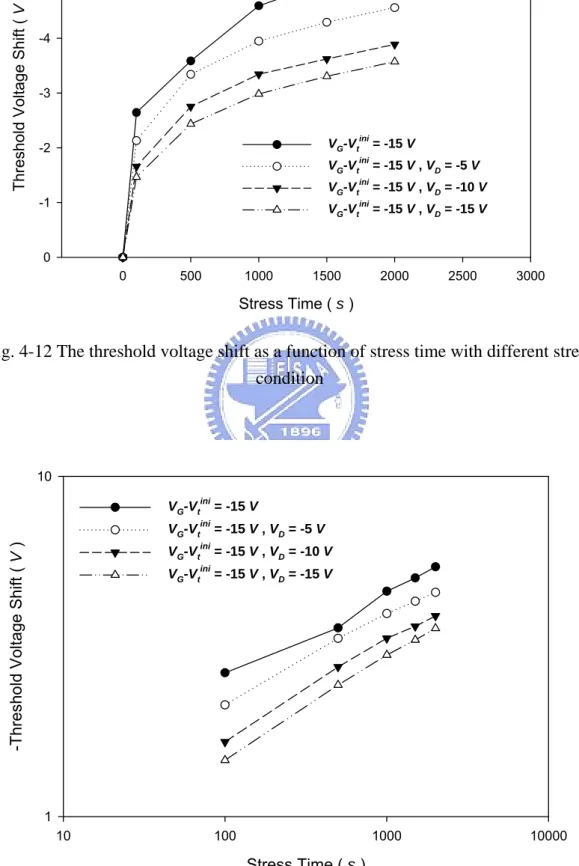
Fig.4-12 The threshold voltage shift as a function of stress time with different stress condition
Fig.4-13 The threshold voltage shift as a function of stress time with different stress on a logarithmic scale condition
Fig.4-14 The res= (Q
T V
[
]
{
ln1 /( )}
log− −ΔVTres VGS−VTini as a function of log(t) in the inset Fig.4-15 The threshold voltage shift as a function of recovery time with different
recovery bias condition
Fig.5-1 The AC signal used in this study
Fig.5-2 The linear-region transfer characteristics of the devices before stress and after effective 2000-sec stress
Fig.5-3 The subthreshold swing and the field-effect mobility as a function of effective stress time with different stress condition
Fig.5-4 The threshold voltage shift as a function of effective stress time Fig.5-6 The threshold voltage shift versus off cycle
Fig.5-7 The RC equivalent circuit to simulate the device under pulsed bias stress Fig.5-8 Normalized threshold voltage shift versus gate bias stress pulse width Fig.5-9 The threshold voltage shift as a function of stress time with different stress
condition
Fig.5-10 The threshold voltage shift as a function of stress time with different stress condition
Fig.5-11 The threshold voltage shift as a function of stress time with different stress condition
Fig.5-12 The threshold voltage shift as a function of stress time with different stress condition
Fig.5-13 The threshold voltage shift as a function of stress time with different stress condition
Chapter 1
Introduction
1-1.
Introduction of Organic Thin Film Transistors (OTFTs)
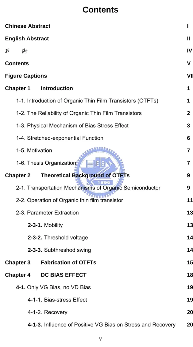
Recently, organic thin-film transistors (OTFTs) have drawn lots of attentions due to their applications on the organic electronics, the radio-frequency identification tags, the electronic papers, and other electronics integrated with organic circuits have been proposed flexible displays [1] [2]. Within a few years, the performances of OTFTs had been improved to be comparable to or better than those of amorphous Si (a-Si) TFTs [3] [4]. Many reports have successfully demonstrated low temperature processes to fabricate low-voltage high-mobility OTFTs. A number of organic materials such as polythiophene, α- sexithiophene (α-6T) have been investigated for use in field effect transistors (FETs) . Polycrystalline molecular solids such as α-sexithiophene (α-6T) or amorphous/semi-crystalline polymers such as polythiophene or acenes such as pentacene, teracene show the highest mobilities[5]. Fig 1.1 shows the evolution of organic materials and the improvement in their mobilities over the years[6]. Pentacene based FETs show the high mobilities and have been extensively studied. Pentacene is made up of five benzene rings as shown in Fig. 1.2 Pentacene has a sublimation
temperature of 300℃. Well ordered pentacene films can be deposited at low temperatures making it suitable for deposition on plastic substrates. However, the reliability issues were still not comprehensively studied. When passivation layers were used to alleviate the device degradation due to the invasion of water vapor or oxygen in the air, the reliability issues under the gate and the drain biases require further investigations[7].
1-2.
The reliability of organic thin film transistors
I t was observed in many reports that the performance of OTFTs degraded under gate bias stress[7] [8]. While the field-effect mobility and the subthreshold swing kept unchanged, threshold voltage shifted severely after the bias stress. The threshold voltage shift is found to be reversible, and is almost not dependent on the dielectric materials[9]. Therefore, the charge trapped in the dielectric layer should not be the reason. On the other hand, the creation of charged defect states in the organic semiconductor layer is proposed to be the underlying mechanism. Moreover, the dependence of the threshold voltage shift on the stressing time is found to follow a stretched-exponential function. It is the same as the bias stress effect in a-Si TFTs. In a-Si TFTs, the generation rate of charged defect is proportional to the
number of carriers, this is known as the defect-pool model[10]. In organic TFTs, J. E. Northrup et al. used density functional calculation to propose that the defect state generation is caused by hydrogen- and oxygen-related defects perturb a carbon atom so as to remove its pz orbital from the π system and give
rise to a state in the gap[11]. They proposed chemical equations to describe these reactions, in which the reaction rate was proportional to the carrier density. They also concluded that the reaction was relative to the bias stress effect.
1-3.
Physical mechanism of bias stress effect
In twenty years ago, the reliability model of amorphous silicon thin film transistors had been studied. Researchers found that the reliability issue came from the threshold voltage (Vth) shift of devices. The characteristic of threshold
voltage shift is the power-law time decay. Therefore the stretched exponential equation is used to describe this phenomenon[12]. The relaxation and dispersive transport of disorder system were often explained by the stretched exponential decay before it was used for describing the threshold voltage shift of amorphous silicon thin film transistors, and the proposed model is valid for any disorder material with a distribution of diffusion-site energy. In resent
experiment, organic material was adopted as the active layer of thin film transistors. Organic thin film transistors (OTFTs) are very potential to fabricate the radio-frequency identification tags, the electronic papers, and the flexible displays. The organic film often was deposited by evaporating or spinning. Therefore it is not prefect single crystal structure; it can be treated as a disorder system. In practice, bias stress effects also restrict the commercial application of OTFTs due to threshold voltage shift. It is interesting that the characteristic of threshold voltage shift is similar to amorphous silicon thin film transistors. Up to now, some studies pointed out that the threshold voltage shift is caused by the state creation and the state creation is governed by a dispersion process. Therefore, they thought that the stretched exponential equation is able to quantify OTFTs stability.
These proposed models described the threshold voltage shift very well, but there are only a few explanations on the micro process of defect generation. Recently the bipolaron mechanism is mentioned. The deep states slowly trap holes to form a bipolaron and the formation of bipolaron would cause the threshold voltage shift due to mobile hole decreasing. The reaction of bipolaron formation can represent.[13] [14].
BP
h
+ →
h
( hh )
+ ++ + → ) ( 2 2h C22H16 C22H14 C22H15 and + 22 16 22 14 22 15 22 15 2h+ +C H O+C H →( C H O )++( C H )
which is mentioned and the mechanism is based on density functional calculation. It is proposed that there are C-H2, OH, and C-HOH defects in
organic semiconductors. These defects may be rise to the bias stress effect. We can find that their mechanisms proposed the defect creation be proportional to carrier concentration. On the defect generation phenomenon studies, the generation and quenching of defect in pentacene is obviously relative to hydrogen diffusion. They thought the relation may be suitable to other organic material[15].
As above mentions, the critical arguments proposed the defect creation rate is proportional to carrier concentration. Therefore, the stretched exponential equation may be verified by applying various drain bias during the gate bias stress. When the carrier concentration in channel was adjusted by various drain bias, the threshold voltage shift was obviously dependent on drain bias. If the data can be fitted very well by considering the channel charge normalization factor, it shows that the state creation rate is proportional to the carrier concentration. The phenomenon is only observed while state creation dominates the threshold voltage shift. Therefore, the main degradation
mechanism of pentacene-based TFTs is state creation which is demonstrated by the modified model.
1-4.
Stretched-exponential Equation
The difference between charge trapping and state creation were explained clearly[10]. When charge trapping dominates, the threshold voltage
shift is logarithmic, th d 0 t V r log 1 t Δ ⎛⎜ + ⎞ ⎝ ∼ ⎟
⎠ . When state creation dominates, the
threshold voltage shift is given by a power law, th 0 t V a t β Δ ⎛⎜ ⎞⎟ ⎝ ⎠
∼ . And Powell also
introduced the stretched-exponential equation G th( ) G th( )
0 t V V t / V V 0 exp t β ⎡⎛ ⎞ ⎤ ⎢ ⎥ ⎡ − ⎤ ⎡ − ⎤= ⎜ ⎟ ⎣ ⎦ ⎣ ⎦ ⎢⎝ ⎠ ⎥ ⎣ ⎦ from DB WB BT 0 BT dN n N D dt N t β
∼ . When the state creation is small, the
stretched-exponential equation approximates to th ( G th) 0 t V V V t β Δ = − ⎛⎜ ⎞⎟ ⎝ ⎠ . The state
creation is small which means t0 >> t. Charge trapping generally needs larger
electrical field than state creation. Even t0 >> t, state creation is still dominated
at low electrical field. The stretched-exponential equation is valid to describe the characteristic of threshold voltage on pentacene based TFTs, and equation
( ) th G th 0 t V V V t β Δ = − ⎛⎜ ⎞⎟
⎝ ⎠ is used fitting the threshold voltage shift[16], when t0 is much
larger. In fact, the amorphous Silicon film is more stable than pentacene film. Therefore th ( G th) 0 t V V V t β Δ = − ⎛⎜ ⎞⎟
1-5.
Motivation
Organic thin film transistor have many advantages, but only a few studies were published in reliability of bias stress. In order to understand, we will discuss under the following topics: DC bias effect and AC bias effect.
It will begin our discussion by considering the DC bias effect inevitably related to the AC bias effect. Thus, we analyze dividedly the gate bias effect with and without drain bias. Because lots of applications of electronic device are operated on different frequency, reliability of organic thin film transistors under AC bias stress is needed to study. So we design experimental condition about frequency and base voltage of pulse.
1-6.
Thesis Organization
In Chapter 1, we describe the introduction of OTFTs, Physical mechanism of bias stress effect, and motivation of the thesis. In Chapter 2, we introduce the transportation mechanisms of organic semiconductor, operation of OTFTs, and parameter extraction. In Chapter 3, the fabrication and the structure of OTFTs are presented. In Chapter 4, gate bias stress effect without drain bias effect, and gate bias stress effect with drain bias effect. In Chapter 5,
frequency effect, AC reliability model, and pulse design. Finally, we describe the conclusion in Chapter 6.
Chapter 2
DEVICES FABRICATION
2-1.
Transportation Mechanisms of Organic Semiconductor
Over the past few years, Carrier transportation in the organic semiconductors have been investigated on the theory and modeling[17]. In the conventional silicon-based semiconductors, carrier transport occurs in delocalized states. However, in the organic materials, carrier transport occurs by hopping of charges between localized states. Organic semiconductors are conjugated materials, where the π-electrons are conducted intra the molecular. Its crystalline is formed by relatively weak Van der Waals interaction between molecules, where the molecular-stacking determines the carrier behavior. There are two major model : “The band-transport model” and “The hopping models” to describe the hopping transport. Band transport should not be suitable for some disordered organic semiconductors, in which carrier transport is govern by the hopping between localized states. Hopping is assisted by phonons and the mobility increases with temperature. Typically, the mobility is very low, usually much lower than 1cm2/V-sec. The boundary between the localized and delocalized processes is taken at a mobility
between 0.1 and 1 cm2/V-sec[18]. Lots of polycrystalline organic semiconductors, including pentacene, rubrene, have room temperature mobility over the boundary[19]. But, temperature-independent mobility was found in some polycrystalline pentacene devices[20]. Therefore, this research indicate that the the whole carrier transport behaviors in high performance polycrystalline pentacene film for such thermal activated hopping process remains a matter to be discussed further. The coherent band-like transport of delocalized carriers becomes the prevalent transport-mechanism in the single crystals of organic semiconductors under the low-temperature environments. The very high hole mobility values have been measured by time-of-flight experiments[21].Thus, the temperature dependence mobility was found below 100K and following with a power law of μ ∝ T-n, n~1, in single crystals of organic semiconductors, consistent with the band-transport model[22]. However, between 100K and 300K, the carrier mobility show a constant value, that has been described as the superposition of two independent carrier transport mechanisms. The first carrier transport mechanism is small molecular polaron. It is formed as a result of interaction of a charge carrier with the intramolecular vibrations of the molecule, on which it is localized during the residence time, with the intramolecular vibrational modes of nearest-neighbour molecules, and move coherently via tunneling. In this small molecular polaron
mechanism, the mobility follows the power law u=aT−n . The other
mechanism is a small lattice polaron, which transport by thermally activated hopping and follow a typical exponential dependence of mobility on temperature law: . The superposition of these two mechanisms has a good results with experimenta of temperature-dependence mobility from room temperature[23]. However, the charge carrier transport in organic molecular crystals is still not well-understood. There is still room for analyzing[24].
a
u=b exp( E / kT )−
2-2.
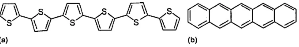
Operation of Organic thin film transistor
There are four basic elements: (i) semiconductor film; (ii) insulating layer; and (iii) source and drain electrode (iv) gate electrode; to be composed a thin film transistor. Actually, the general operation concepts are originated from MOSFET theory. In conventional inorganic thin film transistor, most devices are operated in inversion mode. However, the operation of organic thin film transistor is generally in accumulation mode . The Fermi level of gold and HOMO-LUMO levels of pentacene are shown in Fig. 2-1. When a positive voltage is applied to the gate, the Fermi level of gold is far away from the LUMO level, so that electron injection is very unlikely. therefore, no current
passes through the pentacene layer, and the small measured current essentially comes from leaks through the insulating layer. When the negative voltage is applied to the gate, positive charges are induced in the channel, holes can be injected easily from the source to the semiconductor, because the Fermi level of gold is close to the HOMO level of pentacene. Accordingly, pentacene is said to be a p-type organic semiconductor. However, it need to indicate that this concept differs from conventional semiconductors, which can be made either n-type or p-type by doping mechanism. Symmetrically, an organic semiconductor will be said either n-type or p-type by work function of source is close to HOMO level or LUMO level. The insulator serves as a capacitance per unit area which stores charges and can be represented as , then the accumulated charge per unit area is about . Additionally, assuming that a negligibly small voltage, V
OX
C VGCi
th, is dropped across the
semiconductor. In this situation, the applied drain bias can drive the current from source to drain. The conduction is determined by the mobility which represents the driving ability of the electrical field on the accumulated charges.
In general, It is divide the operation of organic into two regions, linear and saturation regions. The drain current in the linear region is determined from the following equation:
D D TH G OX D V V V V C L W I ) 2 ( − − = μ
where W and L corresponds to the channel width and length,respectively.
Since the drain voltage is quite small, sometimes equation can be simplified as
D TH G OX D C V V V L W I = μ( − )
For , tends to saturate due to the pinch-off of the accumulation layer. The current equation is modified as:
) ( G TH D V V V >− − − ID 2 ) ( 2 OX G TH D C V V L W I = μ −
2-3.
Parameter Extraction
2-3-1. MobilityIn the linear region, mobility can be extracted from the transconductance maximu m gm: D OX t cons V G D m V L WC V I g D μ = ⎥ ⎦ ⎤ ⎢ ⎣ ⎡ ∂ ∂ = = tan
In the saturation region, Mobility can also be extracted from the slope of the curve of the square-root of drain current versus the gate voltage:
D 2L COX(VG VTH) W
2-3-2. Threshold voltage
In the linear region, threshold voltage can be extracted from the current equation of linear region: The intersection point of the drain current versus gate voltage minus 1/2 drain voltage when the device is in the linear mode operation.
In the linear region, threshold voltage can be extracted from the current equation of saturation region:
The intersection point of the square-root of drain current versus gate voltage when the device is in the saturation mode operation.
2-3-3. Subthreshod swing
Subthreshold can also be extracted from
(
)
constant log = ∂ ∂=
D V D GI
V
SChapter 3
Fabrication of OTFTs
The devices used in this series of experiments are the top contact (TC) structure, which means the organic semiconductor layer is deposited on the bottom of the contact electrodes. Below the following sections, we would detail introduce the process of different structures:
Step1. Substrate and gate electrode
4-inch P-type heavily-doped single crystal silicon wafer (100) was used as the substrate and the gate electrode.
Step2. Gate dielectric formation
After the initial RCA cleaning, the 1000Å thermally grown SiO2 layer was
deposited in furnace.
Step3. Pentacene film deposition through the shadow mask[25,26]
The pentacene material obtained from Aldrich without any purification was directly placed in the thermal coater for the deposition. It is well known that
the deposition pressure, deposition rate, and deposition temperature are the three critical parameters to the quality of the organic film. The deposition is started at the pressure around 3×10⁻⁶torr. The deposition rate is controlled at ~0.5Å/sec and the thickness of pentacene film was about 1000Å, monitored by the quartz crystal oscillator. Stable deposition rate is expected to result in smoother and better ordering of the organic molecules. The deposition temperature is also a factor influencing the pentacene film formation. The temperature we use in depositing pentacene films is 70 oC. We use shadow mask to define the active region of each device.
Step4. Source/Drain deposition through the shadow mask[26]
The injection barrier of the OTFT device is determined by the materials of the source and drain electrodes. Materials with large work function are preferred to form Ohmic contact. The Au with work function ~5.1eV does help to provide a better injection. We used shadow mask to define top contact of each device. The top electrodes were Au. Au was deposited on the active layer by ULVAC thermal coater at deposition pressure 3×10⁻⁶ torr. The thicknesses of the metal layer were 1000Å.
In this study, all the measured data were obtained from the semiconductor parameter analyzer (HP 4156A) in the darks at room temperature. And we measure the OTFTs immediately when the samples were unloaded from the evaporation chamber.
Chapter 4
DC BIAS EFFECT
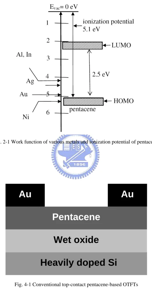
Fig. 4-1 shows the cross-section of the conventional top-contact pentacene-based OTFTs used in this study Firstly, 100-nm-thick thermal oxide was grown on heavily doped Si wafers to serve as the gate dielectric. Then, pentacene obtained from Aldrich without any purification was evaporated through shadow mask onto the thermal oxide to form the active layer. The deposition rate was controlled at 0.5Å/s while the substrate temperature was kept as 70°C. After the formation of 100-nm-thick pentacene, 100-nm-thick gold was deposited through the shadow mask to form the source/drain contacts. The device channel width and length were defined as 1000 μm and 600 μm, respectively. Two series of bias-stress measurements were performed: one with zero drain bias and various gate biases and the other with a fixed gate bias and different drain biases.
4-1.
Only VG bias, no VD bias
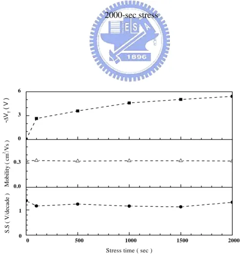
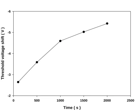
4-1-1. Bias-stress effect
Firstly, we analyze the Bias stress effect with zero drain bias. The linear-region transfer characteristics of the devices before stress and after 2000-sec stress are depicted in Fig. 4-2. With source and drain connected to ground, negative gate biase were used as the stress conditions (VDS = 0 V,
VG – Vthini = -15V), where Vthini is the initial threshold voltage). The negative
gate-bias stress causes a shift of the transfer characteristics while the subthreshold swing stays almost unchanged. The threshold voltage Vth ,
subthreshold swing and the field-effect mobility μFE as a function of stress time
are shown in Fig. 4-3 and Fig. 4-4, respectively. Apparently μFE is not affected
by the stress, while Vth is drastically changed[27] [28]. Such a phenomenon is
often believed to be caused by the generation of deep states with long discharge time that degrade Vth. The shallow traps that would affect μFE may
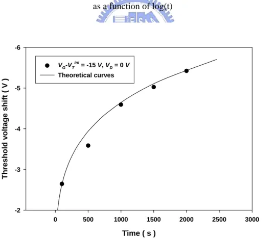
not be changed by the gate bias stress . The power-law dependence between the threshold voltage shift and the stress time is also found in Fig. 4-5. This can be explained by the approximation of the OTFT BSE model, in which the stretched exponential function reduces to the simple power-law function when the stress time is much less than the effective trapping time τ. when the stretched exponential function is used, the dispersion parameter β can be
obtained by plotting log
{
−ln 1⎣⎡ − ΔVT /(VGS −VTini)⎤⎦ as a function of log(t)}
shown in Fig. 4-6. After extracting β = 0.283 and defining the attempt to escape frequency ν = 105 Hz, the effective trapping time τ and the mean activationenergy for the defect generation EA can be determined by fitting with the
stretched exponential function shown in Fig. 4-7 . The resulting E
T V Δ
A is 0.57 eV
and τ is 36127 sec at room temperature.
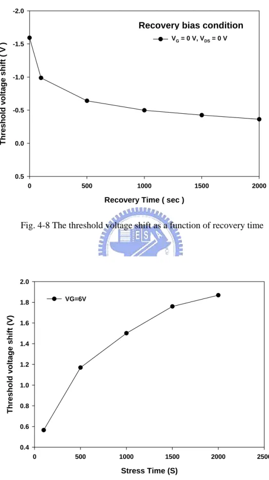
4-1-2. Recovery
Devices subjected to bias stress recover to their original state within a few hours when left in the dark shown in Fig. 4-8 and at the end of the recovery process, the transfer characteristic is essentially identical to that of the unstressed state. The cycle of stress and recovery was repeated with no any change in behavior. Even though the recovery mechanism is still not clearly understood, recombination of the trapped holes with free electrons is proposed to be a plausible reason[29].
4-1-3. Influence of positive VG bias on stress and recovery
Under the same condition as negative gate stress, The stress gate voltage changes to +6V. Because of the presence of pentacene layer at the
source/drain contacts, only the hole conduction characteristics are observed. The characteristics have positive shifts under +6V Bias stress. The evolution of the threshold voltage shift extracted from the curve is shown in Fig. 4-9.As shown in Fig. 4-10, the recovery curves of two identical OTFTs after stress are compared. When the positive gate bias (VGS = +4V) is added to induce
electrons, the recovery of the device is faster than that of the device without positive gate bias. At the 1000s, the threshold voltage shift over the original value become positive under the +4V gate bias and with the discussion in the early part of this section, these results lead us to the conclusion that the positive gate bias not just increase the recovery also include the positive bias effect. This means that electrons can be used to remove defect states or more negative defect states are generated to compensate the threshold voltage shift[29].
4-2.
Fix VG bias stress, various VD bias stress
4-2-1. stress under different VD
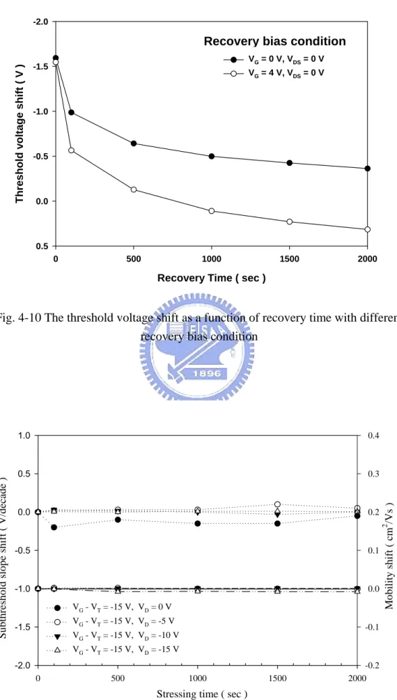
Then, different drain biases (VDS = 0 V, -5 V, -10 V, and -15 V) were added
to the bias-stress measurement while the gate bias was fixed as VG – Vthini =
-15 V. The μFE and the subthreshold swing extracted from devices with
T
Unchanged μFE and subthreshold are observed, and consequently the
influence of drain-bias stress on the shallow traps can be excluded. The influence of drain-bias stress on the Vth, however, is significant. As shown in
Fig. 4-12, the threshold voltage shift ΔVth is suppressed when the drain bias
becomes more negative. All the relationships depicted in Fig. 4-13 follow the power-law dependence with identical slope. According to the BSE model, the slope represents the dispersion parameter β that influences the relaxation and the dispersive transport of disorder system. Identical β value implies that the microscopic processes of the state creation such as the impurity diffusion or the defect creation kinetics should be independent of the drain bias. The influence of drain bias on the carrier concentration is believed, as in a-Si TFTs, to be the dominant reason that causes the ΔVth to be dependent on VDS.
To quantitatively discuss this relationship, for a given VGS, we define the
relative threshold voltage shift rel as the ratio between the ΔV
V
Δ th with
various VDS stress and the ΔVth with zero drain-bias stress. Since the defect
generation rate is proportional to the carrier density, the influence of drain bias on the carrier density in the accumulation channel should be considered. For simplicity, the channel charge normalization factor (QG0/QG) proposed is
⎪⎭ ⎪ ⎬ ⎫ ⎪⎩ ⎪ ⎨ ⎧ ⎥ ⎥ ⎦ ⎤ ⎢ ⎢ ⎣ ⎡ ⎟ ⎠ ⎞ ⎜ ⎝ ⎛ − − − = × Δ β τ t V V Q Q V G Tini G G T ( ) 1 exp 0 where QG0 and QG are expressed as:
(
)
G0 G G T Q =C × ×W L V −V(
) (
(
) (
)
)
3 3 GS T GD T G G 2 2 GS T GD T V V V V 2 Q C W L 3 V V V V − − − = × × − − − The calculated normalized channel charge is defined QG /QG0 , where QGis the channel charge when VD is varied and QG0 is the channel charge when
VDS = 0V. Good agreement can be observed between and the
calculated Q
rel T V Δ
G /QG0 curve. The result verifies the proportionate relationship
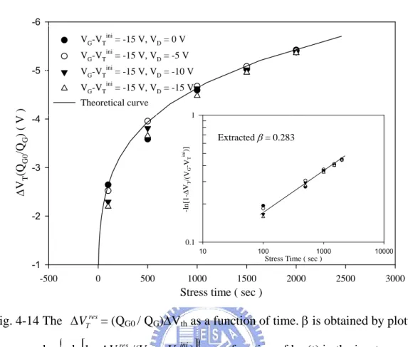
between the defect creation rate and the carrier concentration. Also, the result suggests that convergent data can be obtained by plotting the restored threshold voltage shift res= (Q
T V
Δ G0 / QG)ΔVth as a function of stress time as
shown in Fig. 4-14. The restored threshold voltage shift excludes the drain bias effect and can be used to extract the parameters associated with the defect creation kinetics. For example, when the stretched exponential function is used, the dispersion parameter β can be obtained by plotting
res T V Δ
[
]
{
ln1 /( )}
log− −ΔVTres VGS−VTini as a function of log(t) in the inset of Fig. 4-14.
After extracting β = 0.283 and defining the attempt to escape frequency ν = 105
Hz, the effective trapping time τ and the mean activation energy for the defect generation EA can be determined by fitting ΔVTres with the stretched
exponential function. The resulting EA is 0.57 eV and τ is 36127 sec at room
temperature.
4-2-2. Recovery with VD
Finally, the drain bias effect on the threshold voltage recovery is addressed. It is expected that the positive drain bias reduces the electron amount and suppresses the recovery rate. As shown in Fig. 4-15, the recovery curves of two identical OTFTs after stress are compared. When the same positive gate bias (VGS = 4V) is added to induce electrons, the recovery of the
device without the drain bias is faster than that of the device with a positive drain bias (VDS = 4V). This result gives an insight of the recovery mechanism;
though a comprehensive understanding should be carefully studied in future work.
Chapter 5
AC BIAS STRESS EFFECT
The AC signal used in this study consists of signal amplitudes, frequencies, and duty ratios. We can adjust these parameters and then perform various stress conditions on the gate electrode to realize the instability of Pentacene-based TFTs under different swing regions. Fig. 5-1 shows the waveform of the AC signal. In AC signal, the definition of individual parameter is give as follow:
tc = tp+tb (1)
f = 1/tc (2)
D.R. = tp/tc (3)
Where tc is the signal period, f is the signal frequency and D.R. is the duty ratio.
In the waveform of AC signal, VP is the defined as the peak voltage, while
Vb is defined as the base voltage. The frequency (f) is equal to 1/tc, where the
tc is the signal period and the duty ratio is defined a eq. (3). The tp is the time of
peak voltage and the tb is the time of base voltage. Effective stress time is the
sum of tp. Falling time and rising time are not considered in here because they are very smaller than signal period.
5-1.
Frequency effect
Fig. 5-2 show the evolution of ID-VG characteristics during negative pulsed
bias stress with a duty-cycle of 50% and gate bias pulse width of 2.5ms after effective stress time 2000s at room temperature. The negative pulsed gate bias stress causes a shift of the transfer characteristics while the subthreshold swing and field-effect mobility μFE stays almost unchanged similar with DC bias
stress effect. The threshold voltage Vth , subthreshold swing and the
field-effect mobility μFE as a function of stress time are shown in Fig. 5-3 and
Fig. 5-4, respectively. Fig. 5-5 shows the threshold voltage shift versus effective stress time under negative pulse bias stress for different pulse conditions. The effective stress time is the accumulated time when the gate voltage is high(ON). Threshold voltage shift has strong frequency dependence-the higher frequency, the smaller the magnitude of threshold voltage shift. There are two possible reasons to explain the phenomenon. (1) OFF region: The state creation defects were recovered during OFF cycle region. (2) ON region: The effective concentration dominates the pulsed bias stress dependence of threshold voltage shift.
5-2.
AC reliability model
5-2-1. off-cycle effect
Because the recovery rate of defects in pentacene is faster than defects in amorphous silicon, the effect of OFF cycle region must be considered. In section 4-1-2 shows the threshold voltage shift decreases fast after removing the bias stress. In order to demonstrate recovery effect, the fixed ON region combine various OFF region to form various duty cycle. Fig. 5-6 shows the threshold voltage shift do not dependent on the OFF region.
5-2-2. Equivalent circuit
In order to analyze the apparent pulse width dependent threshold voltage shift for negative pulsed bias stress effect, we used an simple RC equivalent circuit to simulate the device under negative pulsed bias stress. The RC circuit consists of the insulator capacitance Ci, pentacene capacitance Cs, and a
effective pentacene resistance Rs for hole conduction and injection, as shown
in Fig. 5-7. After applying a gate pulse with amplitude VST is expressed as[30]
[31] )] exp( 1 [ ) ( * * RC s i i ST i t C C C V t V τ − + − =
accumulation along the pentacene/oxide interface. The accumulated hole
concentration along the pentacene/oxide interface can be expressed asNaccum =−Ni+Ns where Ni=CiVi/q,Ns=CsVs/q .And by VST=Vi+Vs we can
derive
The average accumulated hole concentration, NAC during a pulse width
time can be expressed as
∫
= − + − = PW RC RC RC DC AC PW PW PW N dt t N PW N 0 * * )] exp( 1 [ ) ( 1 τ τ τWhere NDC is the accumulated hole concentration under DC gate bias
stress. According to the section 4-2-1, the threshold voltage shift under the negative bias stress is proportional the carrier concentration, the relationship between DC stress and AC stress induced the threshold voltage shift with the same effective stress time can be expressed as
) exp( 1 RC RC RC DC T AC T PW PW PW V V τ τ τ + − − = Δ Δ
where ∆VthAC and ∆VthDC are threshold voltage shift by AC stress and DC
stress, respectively. )] V V ( C V C [ q 1 ) V C V C ( q 1 Ns Ni N =− + = − i i+ s s = − i i + s ST − i )]} exp( 1 )[ )( ( { 1 * RC s i i ST i s ST s t C C C V C C V C q N τ − + − − + + = ⇒ )] t exp( C ) C C ( V V C [ q 1 RC * i i s ST ST s − + + −τ = ] 1 ) t [exp( q V C RC * ST i − τ − =
5-2-3. pulse width effect
The degree of threshold voltage shift is decided by ON region. If off region do not affect the dependent, the on region decide the direct. Section 5-2-2 used effective carrier model to explain the threshold voltage shift decreasing with pulse width increasing. Fig. 5-8 shows the experiment threshold voltage and theoretical curve as a function of pulse width at effective stress time of 2000s , τRC ≒ 15us per unit area for 100nm thick pentacene. This result
discussed the threshold voltage shift under various pulse width along with the pulsed gate bias stress when the defect creation was the dominant mechanism. Similar to the DC bias stress model, the defect generation rate in AC bias stress was proportional to the carrier density. Therefore, a effective channel carrier normalization factor was used to describe the pulse width effect and to modify the conventional stretched-exponential function. Good agreement was achieved between the theoretical equation and the experimental results.
5-3.
Pulse design
5-3-1. Off-state bias stress effect
In order to examine the Vb adjustment effect of the bipolar bias stress,it will be useful to analyze the positive pulsed bias stress. The Fig. 5-9 shows
that the time dependence of the threshold voltage shift which caused by the positive AC stress compared with positive DC bias stress. For positive pulse bias stress, the threshold voltage shifts are significant smaller in comparison with threshold voltage shift induced by positive DC gate bias stress. This result can be explained by considering the characteristic of pentacene-based TFTs. Au was used as drain and source on pentacene layer. The Fig. 2-1 shows the work function of Au is near the LOMO band of pentacene. When the positive bias was applied, the interface of Au/pentacene would induce a large barrier to impede electron injection. During positive AC bias stress, the on region time of period is effective time to accumulate electrons. The interface barrier makes a huge barrier to induce huge RC delay time generation. Although electrons are easily to cause defects, there is not enough time to accumulate electrons.
5-3-2. Vb adjustment
F ig. 3-10 shows the threshold voltage shift induced by negative (VG – Vthini
= -20V) pulsed bias stress and bipolar pulsed bias stress by various base voltage of negative (VG – Vthini = -20V) and positive (Vb = +6V, +8V, +10V) with
the same 50% duty cycle and 2.5ms pulse width. The threshold voltage shift of bipolar pulse bias stress with Vb=+6V is slightly small than that for negative
section 5-3-1, it was pointed out that the threshold voltage shifts of positive pulsed bias stress are significant smaller in comparison with threshold voltage shift induced by positive DC gate bias stress, but actually have small shift. Therefore, it seems reasonable to conclude that the threshold voltage shift of bipolar pulsed bias stress is combined the effect of negative and positive pulsed bias stress together.
5-3-3. frequency adjustment
With various pulse width (2.5ms, 100us, 50us), the threshold voltage shift induced by negative (VG – Vthini = -20V) pulsed bias stress and bipolar pulsed
bias stress of negative (VG – Vthini = -20V) and positive (Vb = +8V) are shown in
Fig. 5-11, Fig. 5-12 and Fig. 5-13, respectively. The threshold voltage shift of bipolar pulse bias stress with Vb=+8V is small than that for negative pulsed
bias stress with different pulse width. This result provided one more evidence for that the threshold voltage shift of bipolar pulsed bias stress is combined the effect of negative and positive pulsed bias stress together.
Chapter 6
CONCLUTION
6-1.
DC bias effect
This chapter discussed the threshold voltage shift under various drain biases along with the gate bias stress when the defect creation was the dominant mechanism. Similar to the defect pool model in a-Si TFTs, the defect generation rate in OTFTs was proportional to the carrier density. Therefore, a channel charge normalization factor was used to describe the influence of drain bias and to modify the conventional stretched-exponential function. Good agreement was achieved between the modified equation and the experimental results.
6-2.
AC bias effect
The instability of OTFTs under various AC biases was investigated. Firstly, the state creation governed by the defect pool model is found to be dominant under the bias stress. Calculating the effective channel carrier concentration considering the RC delay can successfully explain the dependence of threshold voltage shift on the frequency or on the pulse width of the stressing signal. It was also found that in AC stress, only holes contribute
to defect creation, electrons may not exist due to their large charging time through the high injection barrier. Finally, by changing the base voltage in the AC stressing signal, the threshold voltage shift can be modified since the effect of negative and positive pulsed bias stress together.
References
[1] K. Nomoto, N. Hirai, N. Yoneya et al., "A high-performance short-channel bottom-contact OTFT and its application to AM-TN-LCD," IEEE Trans. Electron Devices 52 (7), 1519-1526 (2005).
[2] M. Mizukami, N. Hirohata, T. Iseki et al., "Flexible AM OLED panel driven by bottom-contact OTFTs," IEEE Electron Device Lett. 27 (4), 249-251 (2006).
[3] H. Klauk, M. Halik, U. Zschieschang et al., "High-mobility polymer gate dielectric pentacene thin film transistors," J. Appl. Phys. 92 (9), 5259-5263 (2002).
[4] W. Wang, J. W. Shi, W. H. Jiang et al., "High-mobility pentacene thin-film transistors with copolymer-gate dielectric," Microelectron. J. 38 (1), 27-30 (2007).
[5] H. E. Katz, C. Kloc, V. Sundar et al., "Field-effect, transistors made from macroscopic single crystals of tetracene and related semiconductors on polymer dielectrics," J. Mater. Res. 19 (7), 1995-1998 (2004).
[6] C. D. Dimitrakopoulos and D. J. Mascaro, "Organic thin-film transistors: A review of recent advances," IBM J. Res. Dev. 45 (1), 11-27 (2001). [7] H. L. Gomes, P. Stallinga, F. Dinelli et al., "Electrical characterization of
organic based transistors: stability issues," Polym. Adv. Technol. 16 (2-3), 227-231 (2005).
[8] J. B. Chang and V. Subramanian, "Effect of active layer thickness on bias stress effect in pentacene thin-film transistors," Appl. Phys. Lett. 88 (23) (2006).
[9] A. Salleo and R. A. Street, "Light-induced bias stress reversal in polyfluorene thin-film transistors," J. Appl. Phys. 94 (1), 471-479 (2003). [10] M. J. Powell, C. Vanberkel, and J. R. Hughes, "Time And
Temperature-Dependence Of Instability Mechanisms In Amorphous-Silicon Thin-Film Transistors," Appl. Phys. Lett. 54 (14), 1323-1325 (1989).
[11] J. E. Northrup and M. L. Chabinyc, "Gap states in organic semiconductors: Hydrogen- and oxygen-induced states in pentacene," Phys. Rev. B 68 (4) (2003).
[12] J. Kakalios, R. A. Street, and W. B. Jackson, "Stretched-Exponential Relaxation Arising From Dispersive Diffusion Of Hydrogen In Amorphous-Silicon," Phys. Rev. Lett. 59 (9), 1037-1040 (1987).
[13] R. A. Street, A. Salleo, and M. L. Chabinyc, "Bipolaron mechanism for bias-stress effects in polymer transistors," Phys. Rev. B 68 (8) (2003).
[14] A. Salleo and R. A. Street, "Kinetics of bias stress and bipolaron formation in polythiophene," Phys. Rev. B 70 (23) (2004).
[15] D. V. Lang, X. Chi, T. Siegrist et al., "Bias-dependent generation and quenching of defects in pentacene," Phys. Rev. Lett. 93 (7) (2004). [16] K. S. Karim, A. Nathan, M. Hack et al., "Drain-bias dependence of
threshold voltage stability of amorphous silicon TFTs," IEEE Electron Device Lett. 25 (4), 188-190 (2004).
[17] R. A. Street, D. Knipp, and A. R. Volkel, "Hole transport in polycrystalline pentacene transistors," Appl. Phys. Lett. 80 (9), 1658-1660 (2002).
[18] G. Horowitz, "Organic field-effect transistors," Adv. Mater. 10 (5), 365-377 (1998).
[19] Y. Y. Lin, D. J. Gundlach, S. F. Nelson et al., "Stacked pentacene layer organic thin-film transistors with improved characteristics," IEEE Electron Device Lett. 18 (12), 606-608 (1997).
[20] S. F. Nelson, Y. Y. Lin, D. J. Gundlach et al., "Temperature-independent transport in high-mobility pentacene transistors," Appl. Phys. Lett. 72 (15), 1854-1856 (1998).
[21] W. Warta and N. Karl, "Hot Holes In Naphthalene - High, Electric-Field-Dependent Mobilities," Phys. Rev. B 32 (2), 1172-1182 (1985).
[22] L. B. Schein, C. B. Duke, and A. R. McGhie, "Observation Of Band-Hopping Transition For Electrons In Naphthalene," Phys. Rev. Lett. 40 (3), 197-200 (1978).
[23] E. A. Silinsh, A. Klimkans, S. Larsson et al., "Molecular Polaron States In Polyacene Crystals - Formation And Transfer Processes," Chem. Phys. 198 (3), 311-331 (1995).
[24] O. Ostroverkhova, D. G. Cooke, S. Shcherbyna et al., "Bandlike transport in pentacene and functionalized pentacene thin films revealed by subpicosecond transient photoconductivity measurements," Phys. Rev. B 71 (3) (2005).
[25] C. D. Dimitrakopoulos, A. R. Brown, and A. Pomp, "Molecular beam deposited thin films of pentacene for organic field effect transistor applications," J. Appl. Phys. 80 (4), 2501-2508 (1996).
[26] C. W. Chu, S. H. Li, C. W. Chen et al., "High-performance organic thin-film transistors with metal oxide/metal bilayer electrode," Appl. Phys. Lett. 87 (19) (2005).
[27] H. L. Gomes, P. Stallinga, F. Dinelli et al., "Bias-induced threshold voltages shifts in thin-film organic transistors," Appl. Phys. Lett. 84 (16), 3184-3186 (2004).
[28] D. Kawakami, Y. Yasutake, H. Nishizawa et al., "Bias stress induced threshold voltage shift in pentacene thin-film transistors," Jpn. J. Appl. Phys. Part 2 - Lett. Express Lett. 45 (42-45), L1127-L1129 (2006). [29] D. Knipp, R. A. Street, A. Volkel et al., "Pentacene thin film transistors
on inorganic dielectrics: Morphology, structural properties, and electronic transport," J. Appl. Phys. 93 (1), 347-355 (2003).
[30] R. Oritsuki, T. Horii, A. Sasano et al., "Threshold Voltage Shift Of Amorphous-Silicon Thin-Film Transistors During Pulse Operation," Japanese Journal Of Applied Physics Part 1-Regular Papers Short Notes & Review Papers 30 (12B), 3719-3723 (1991).
[31] C. S. Chiang, J. Kanicki, and K. Takechi, "Electrical instability of hydrogenated amorphous silicon thin-film transistors for active-matrix liquid-crystal displays," Japanese Journal Of Applied Physics Part 1-Regular Papers Short Notes & Review Papers 37 (9A), 4704-4710 (1998).
Figures
Fig. 1.1. Semilogarithmic plot of mobility vs.year.
Fig. 2-1 Work function of various metals and ionization potential of pentacene.
Fig. 4-1 Conventional top-contact pentacene-based OTFTs
Au
Au
Pentacene
Wet oxide
Fig. 4-2 The linear-region transfer characteristics of the devices before stress and after 2000-sec stress
Fig. 4-3 The threshold voltage shift, subthreshold swing and the field-effect mobility
VG ( V ) -40 -30 -20 -10 0 10 20 -Drai n Cu rrent ( A ) 10-12 10-11 10-10 10-9 10-8 10-7 10-6 10-5 -Drain Cur rent ( μ A ) 0 1 2 3 4 Initial After stress 2000s 0 500 1000 1500 2000 0 1
Stress time ( sec )
S. S ( V/ d ec ad e ) 0.0 0.3 Mo bilit y ( cm 2 /V s ) 0 3 6 -Δ VT ( V )
as a function of stress time
Fig. 4-4 The threshold voltage shift as a function of stress time on a linear scale
Fig. 4-5 The threshold voltage shift as a function of stress time on a logarithmic scale
Time ( s ) 0 500 1000 1500 2000 2500 Threshold v o ltage shift ( V ) -6 -5 -4 -3 -2 Time ( s ) 10 100 1000 10000 -Th resho ld v o ltage shi ft ( V ) 1 10
Time ( s ) 10 100 1000 10000 -l n[1-Δ VT /(V G -V T in i )] 0.1 1 β = 0.283
Fig. 4-6 The dispersion parameter β obtained by plotting log
{
−ln 1⎣⎡ − ΔVT /(VGS−VTini)⎤⎦}
as a function of log(t) Time ( s ) 0 500 1000 1500 2000 2500 3000 Thresh old v o ltage sh ift ( V ) -6 -5 -4 -3 -2 VG-VT ini = -15 V, VD = 0 V Theoretical curvesFig. 4-7 The threshold voltage shift as a function of stress time. Circle denote experimental measurements and solid line denote theoretical curves.
Recovery bias condition
Recovery Time ( sec )
0 500 1000 1500 2000 T h res hold v o lt ag e s h ift ( V ) -2.0 -1.5 -1.0 -0.5 0.0 0.5 VG = 0 V, VDS = 0 V
Fig. 4-8 The threshold voltage shift as a function of recovery time
Stress Time (S) 0 500 1000 1500 2000 2500 Thre s ho ld volta ge sh if t (V) 0.4 0.6 0.8 1.0 1.2 1.4 1.6 1.8 2.0 VG=6V
Recovery bias condition
Recovery Time ( sec )
0 500 1000 1500 2000 T h res hold v o lt ag e s h ift ( V ) -2.0 -1.5 -1.0 -0.5 0.0 0.5 VG = 0 V, VDS = 0 V VG = 4 V, VDS = 0 V
Fig. 4-10 The threshold voltage shift as a function of recovery time with different recovery bias condition
Stressing time ( sec )
0 500 1000 1500 2000
Su
bthreshold slope shift
( V/ decade ) -2.0 -1.5 -1.0 -0.5 0.0 0.5 1.0 M o bi lity shift ( cm 2 /V s ) -0.2 -0.1 0.0 0.1 0.2 0.3 0.4 VG - VT = -15 V, VD = 0 V VG - VT = -15 V, VD = -5 V VG - VT = -15 V, VD = -10 V VG - VT = -15 V, VD = -15 V
Fig. 4-11 The subthreshold swing and the field-effect mobilityas a function of stress
time with different stress condition
Stress Time ( s ) 0 500 1000 1500 2000 2500 3000 Thr eshold Voltage Shift ( V ) -6 -5 -4 -3 -2 -1 0 VG-Vtini = -15 V VG-Vtini = -15 V , VD = -5 V VG-Vtini = -15 V , VD = -10 V VG-Vtini = -15 V , VD = -15 V
Fig. 4-12 The threshold voltage shift as a function of stress time with different stress condition Stress Time ( s ) 10 100 1000 10000 -Thresh o ld Vo ltag e S h ift ( V ) 1 10 VG-Vt ini = -15 V VG-Vtini = -15 V , VD = -5 V VG-Vt ini = -15 V , VD = -10 V VG-Vt ini = -15 V , VD = -15 V
on a logarithmic scale condition
Stress time ( sec )
-500 0 500 1000 1500 2000 2500 3000 ΔV T (Q G0 /Q G ) ( V ) -6 -5 -4 -3 -2 -1 VG-VTini = -15 V, VD = 0 V VG-VTini = -15 V, VD = -5 V VG-VTini = -15 V, VD = -10 V VG-VTini = -15 V, VD = -15 V Theoretical curve
Stress Time ( sec )
10 100 1000 10000 -l n[ 1-ΔV T /( VG -V T in i)] 0.1 1 Extracted β = 0.283
Fig. 4-14 The ΔVTres= (QG0 / QG)ΔVth as a function of time. β is obtained by plotting
[
]
{
ln1 /( )}
log− −ΔVTres VGS −VTini as a function of log(t) in the inset
Recovery bias condition
Recovery Time ( sec )
0 500 -2.0 -1.5 -1.0 -0.5 0.0 0.5 VG = 0 V, VDS = 0 V VG = 4 V, VDS = 0 V Threshold v olta ge sh ift ( V ) VG = 4 V, VDS = 4 V 1000 1500 2000
recovery bias condition
Time
( s )
Voltage ( V )
V
pV
bt
pt
bFig. 5-1 The AC signal used in this study
Fig. 5-2 The linear-region transfer characteristics of the devices before stress and after effective 2000-sec stress
VG ( V ) -40 -30 -20 -10 0 10 20 -Drain Current ( A ) 10-12 10-11 10-10 10-9 10-8 10-7 10-6 10-5 -Drain Current ( μ A ) 0 2 4 6 Initial After stress 2000s
Effective stress time(S) 0 500 1000 1500 2000 Subthreshold slope ( V/decade ) -2 -1 0 1 Mob il ity (cm 2 /V s ) -0.2 -0.1 0.0 0.1 0.2 0.3 0.4 DC PW = 2.5ms D.R=50% PW = 100us D.R=50% PW = 50us D.R=50% PW = 10us D.R=50% PW = 3us D.R=50%
Fig. 5-3 The subthreshold swing and the field-effect mobilityas a function of effective stress time with different stress condition
Effective Stress Time (S)
0 500 1000 1500 2000 2500 Th reshold v oltag e shift ( V ) -8 -6 -4 -2 0 PW=2.5ms D.R=50%
Effective Stress Time (S) 0 500 1000 1500 2000 2500 Thres hold v oltag e shift ( V ) -8 -6 -4 -2 0 DC PW=2.5ms D.R=50% PW=100us D.R=50% PW=50us D.R=50% PW=10us D.R=50% PW=3us D.R=50%
Fig. 5-5 The threshold voltage shift as a function of effective stress time with different stress condition Off cycle (ms) 0 5 10 15 20 25 Threshold v o ltage shift (V) -3.0 -2.5 -2.0 -1.5 -1.0
Qs Rs Qi Ci Cs Gate Source PW Period 0V VST t*
Fig. 5-7 The RC equivalent circuit to simulate the device under pulsed bias stress
Pulse Width (S) 10-7 10-6 10-5 10-4 10-3 10-2 Δ V t AC /Δ V t DC 0.0 0.2 0.4 0.6 0.8 1.0 1.2 experiment Theoretical curves
E ffective S tress T im e (S ) 0 500 1000 1500 2000 2500 Threshol d v o lt age s h ift ( V ) 0.0 0.5 1.0 1.5 2.0 D C P W =2.5m s D .R =50% P W =100u s D .R =50% P W =50u s D .R =50% P W =10u s D .R =50% P W =3u s D .R =50%
Fig. 5-9 The threshold voltage shift as a function of stress time with different stress condition
Effective Stress time (S)
10 100 1000 10000 Threshol d Vol tage shift (V) -6 -5 -4 -3 -2 -1 0 Vg-Vt=-20V PW=2.5ms Vg-Vt=-20V PW=2.5ms Vb=8V Vg-Vt=-20V PW=2.5ms Vb=6V Vg-Vt=-20V PW=2.5ms Vb=10V
Fig. 5-10 The threshold voltage shift as a function of stress time with different stress condition
Effective Stress time (S) 10 100 1000 10000 T h re s hold Volt ag e sh ift (V) -6 -5 -4 -3 -2 -1 0 Vg-Vt=-20V PW=2.5ms Vg-Vt=-20V PW=2.5ms Vb=8V
Fig. 5-11 The threshold voltage shift as a function of stress time with different stress condition
Effective Stress time (S)
10 100 1000 10000 Th resh ol d V o lt ag e shift (V ) -6 -5 -4 -3 -2 -1 0 Vg-Vt=-20V PW=100us Vg-Vt=-20V PW=100us Vb=8V
Fig. 5-12 The threshold voltage shift as a function of stress time with different stress condition
Effective Stress time (S) 10 100 1000 10000 Threshold Volt age shif t ( V ) -6 -5 -4 -3 -2 -1 0 Vg-Vt=-20V PW=50us Vg-Vt=-20V PW=50us Vb=8V
Fig. 5-13 The threshold voltage shift as a function of stress time with different stress condition