Thermal conductance and the Peltier coefficient of carbon nanotubes
M. F. Lin and D. S. ChuuElectrophysics Department, National Chiao Tung University, Hsinchu 30050, Taiwan, Republic of China
K. W.-K. Shung
Physics Department, National Tsing Hua University, Hsinchu 30043, Taiwan, Republic of China ~Received 11 September 1995; revised manuscript received 27 November 1995!
Thep-band structure of one-dimensional carbon nanotubes is very special. Their ballistic transport proper-ties are studied theoretically and are found to exhibit rich magnetic-flux-dependent structures. The thermal conductancek(f) has many step structures caused by the Zeeman splitting; a similar effect has been found in the electrical conductance G(f). The Peltier coefficient P(f) vanishes in the zero-voltage limit at any magnetic flux due to the symmetricp-band structure about the chemical potential m50. However, a finite Peltier effect could be observed by applying a finite voltage or by doping carbon nanotubes. Doping also causes peak structures with quantized maxima inP(f), as well as more step structures in k(f). Both the quantized peaks and the steps should be observable at T,1 K. These structures and also the validity of Wiedemann-Franz lawk(f)'p2kB
2
TG(f)/3e2are found to depend upon the temperature, the chemical po-tential, thep-band property, and the Zeeman effect.
I. INTRODUCTION
The cylindrically coaxial carbon nanotubes recently re-ported by Iijima1 have radii between 10 and 150 Å. This class of one-dimensional ~1D! system has stirred a lot of recent studies.2–20One of the important advancements in ex-periments is that the single-shell carbon nanotubes could be produced in large-scale synthesis and their radii cover a wide range from 3.5 to 30 Å.2,3A single-shell carbon nanotube is predicted to be either a metal or a semiconductor,4–8 depend-ing on its radius and chirality. Furthermore, it could change drastically from being a metal~semiconductor! to a semicon-ductor ~metal! as the magnetic flux f ~Ref. 7! through the nanotubes varies. The transport properties directly reflect the band property near the Fermi level. Hence transport mea-surements on a carbon nanotube could be used to test the validity of predicted band properties. The electrical conduc-tance of a carbon nanotube has been studied theoretically within the ballistic regime.11,12In this work we further inves-tigate the thermal and thermoelectric properties by evaluat-ing the thermal conductance k and the Peltier coefficient P as a function of f. The effects due to the Zeeman splitting, temperature, bias voltage, and doping are included in the study.
There are some transport measurements13–15 on carbon nanotubes in the bundle form. These measurements show that such a three-dimensional~3D! bundle structure exhibits different transport properties. For example, the temperature-dependent resistivity varies logarithmically at lower temperature,13 drops off quickly at higher temperature,13,14 and exhibits a strong anisotropy between the parallel and perpendicular directions with respect to the tubular axis.15It is difficult to identify the p-band properties or to examine the theoretical predictions4–8 from these measurements be-cause the measured nanotube bundles are made up of differ-ent single-shell and multishell nanotubes. On the theoretical side, the electron-phonon scattering16is evaluated to estimate
the electrical conductivity of carbon nanotubes and the electron-impurity scattering17 could explain, qualitatively, the logarithmic temperature dependence in resistivity.
In this work, we mainly study the electric and thermal currents through a single-shell carbon nanotube within the ballistic regime. In low-dimensional systems, the ballistic electrical conductance exhibits the quantized step structures, which were studied by Landauer.21Streda22further predicted the quantized nature of thermoelectric properties such as in thermopower S. On the experimental side, the quantized transport properties in electrical conductance G,23,24
thermopower,25Peltier coefficientP,26and thermal conduc-tancek ~Ref. 26! have all been identified in many systems. Carbon nanotubes, being a 1D system, should also exhibit these quantization phenomena.12 Such behaviors are basi-cally caused by the heat- and current-carrying subbands close to the Fermi level EF50. The carbon nanotube considered
here is, in the presence of a uniform magnetic field B, along the tubular axis. The interaction12,18,19between the spin and the B field is taken into account so that the subbands could cross and intersect the Fermi level within a certain magnetic-flux range.12,19As a result, thef-dependent thermal conduc-tance exhibits step structures. Our calculations are performed at various temperatures so that we can find out under which conditions the step structures are observable and the approxi-mated Wiedemann-Franz ~WF! law k(f)'p2kB2TG(f)/ 3e2 is valid. Since the conduction bands are symmetric, about EF50, to the valence bands, the f-dependent Peltier
coefficient and thermopower are found to vanish at any mag-netic flux in the zero-voltage limit. Therefore, a finite bias voltage27is needed in study of the Peltier effect.
Doping could also induce quantized structures in k(f) andP(f). The alkali-metal atoms K and Rb~Ref. 20! have been successfully intercalated into carbon nanotubes, as done for graphite intercalation compounds28 ~GIC’s! and carbon fibers.29 Electrons in these cases are transferred from the intercalants to the carbon nanotubes; the Fermi energy thus 53
increases from zero to a finite value.8,19There are many heat-and current-carrying 1D subbheat-ands intersecting with the Fermi level. When the Fermi level crossing takes place,
k(f) andP(f) are expected to exhibit, respectively, a step structure and a peak structure with a quantized maximum.22,30,31Doped carbon nanotubes are found to dis-play richer quantized structures as the magnetic flux varies, which suggests that the experimental verification of the bal-listic behavior may be easier after doping.
This paper is organized as follows. The ballistic transport of a carbon nanotube in the presence of a uniform B field is discussed in Sec. II. The thermal conductance and the Peltier coefficient are calculated in Sec. III. Here the effects due to Zeeman splitting, temperature, bias voltage, and doping are also discussed. Finally, concluding remarks are presented in Sec. IV.
II. BALLISTIC TRANSPORT IN A UNIFORM B FIELD The geometric structure of a carbon nanotube could be regarded as a rolled-up graphite sheet in the cylindrical form ~Fig. 1 in Ref. 12!. A carbon nanotube may be uniquely characterized by using a 2D lattice vector Rx5ma11na2, where a1 and a2 are primitive lattice vectors of a graphite sheet. A carbon nanotube represented by (m,n) has a chiral angle u5tan21@2
A
3n/(2m1n)# and a radius r5uRxu/2p5b
A
3(m21mn1n2)/2p. b51.42 Å is the nearest-neighbor distance. It is sufficient to take a zigzag nanotube denoted by (m,0), with u50°, as a model study in under-standing the essential characteristics of transport properties.The (m,0) nanotube here exists in a uniform B field par-allel to the tubular axis (iey). Thep-band structure is
cal-culated within the tight-binding model like the one employed for a graphite sheet.32The energy dispersion is given by6,12
E~J,ky,s,f!5E~J,ky,f!1E~s,f!, ~1a!
where E~J,ky,f!56g0
H
114 cosS
3bky 2D
cosF
p mS
J1 f f0DG
14 cos2F
p mS
J1 f f0DGJ
1/2 , ~1b!with the resonance integral g053.033 eV ~Ref. 6! and
E~s,f!5 gs
m*r2 f f0
. ~1c!
The only effect of the B field is to change the angular mo-mentum ~the subband index! from J (J51,2, . . . ,2m) to
J1f/f0. The axial wave vector ukyu<p/3b is confined
within the first Brillouin zone. The spin-B interaction
E(s,f)5(gs/m*r2)(f/f0), where the g factor is the same as that (.2) of the pure graphite or GIC’s,28 s5612 is the electron spin, and m* is the bare electron mass. When
E~s,f! is neglected, a ~m,0! nanotube with m53I ~Þ3I ! is metallic7,12 at fa5If0 @(I 6
1
3)f0#, where I denotes an integer; it is semiconducting at otherf’s. Under these con-ditions ~i.e., f5fa), EF50 touches both the conduction
and the valence bands but only at the band edges. However, the spin-B interaction could cause the subbands to cross the Fermi level in the neighborhood of fa,
12,19
and its magni-tude is estimated to be much larger than the energy gap due to the mixing effect6of the p ands bands and the Peierls distortion.6,7Hence, with the Zeeman effect taken into con-sideration, a carbon nanotube is metallic within a certain magnetic-flux range near fa. This feature leads to step
structures in the ballistic thermal conductance. The p-band structure @Eqs. ~1a!–~1c!#, where the conduction and the va-lence bands are symmetric about EF50, on the other hand, results in a vanishing Peltier coefficient P(f)50 at zero bias voltage.
The system under consideration is a single-shell zigzag nanotube threaded by a magnetic fluxf and suspended be-tween two macroscopic leads ~energy and particle reser-voirs!. When the bias voltage V and the temperature differ-ence DT are applied between the two reservoirs, the electric and the thermal currents will flow through the carbon nano-tube. The left and the right reservoirs are assumed to have the chemical potentials and the temperatures (m1eV,T) and (m,T1DT), respectively, at which the electrons obey the Fermi-Dirac statistics. The chemical potential here needs to satisfy the condition27,11 eV1m>EF>m, where EF is the
Fermi energy of the carbon nanotube.m5EF is taken in the calculations even in cases when VÞ0.12 In the ballistic re-gime, the length of the nanotube needs to be shorter than the elastic and the inelastic mean free path, i.e., there should be no scattering inside the nanotube. The ballistic quantization effects are important only at T,2 K ~see later!. The inelastic mean free path at such a low-temperature range is estimated to be larger than 1 mm.16 A nanotube of this length, made essentially impurity free, should be suitable for ballistic transport measurements. Furthermore, inelastic scattering is assumed to occur only in the reservoirs, and strong elastic scattering at the contacts between the carbon nanotube and the leads. After detailed derivations,33 the net electric and thermal currents are, respectively, given by
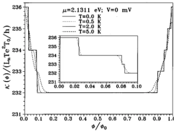
FIG. 1. Thermal conductancek(f)/(LnTe
2
T0/h) of the~210,0!
nanotube at V50 mV andm50 eV, calculated at various tempera-tures. The electrical conductance is also shown in the inset for comparison.
I~f!5eT0
(
J,sE
ky.0 dky 2p 1 \U
]E ]kyU
H
f0S
E2m2eV TD
2 f0S
E2m T1DTDJ
~2a! and U~f!5T0(
J,sE
ky.0 dky 2p 1 \U
]E ]kyU
~E2m!H
f0S
E2m2eV TD
2 f0S
E2m T1DTDJ
, ~2b!where E5E(J,ky,s,f)@Eq. ~1a!#. (1/\)u]E/]kyu is the
lon-gitudinal velocity, T0 @see Eq. ~4! in Ref. 33# the net prob-ability for electrons in the reservoirs to enter a carbon nano-tube with the above velocity, and f0 the Fermi-Dirac distribution function for electrons deep inside the reservoirs.
T051 in the absence of scattering at contacts.
When there is no temperature difference between two res-ervoirs, the Peltier coefficient is defined as34
P~f!5UI~~ff!!
U
DT50
~3! in the vanishing bias voltage (V→0) limit. Withm50, the thermal current from the left reservoir is equal to that from the right reservoir @see Eqs. ~2b! and ~4b!#, owing to the symmetry of thep bands about m50. The net thermal cur-rent through an undoped carbon nanotube thus vanishes at any magnetic flux, and so does the Peltier coefficient. We note that the net electric current12 through an undoped car-bon nanotube does not necessarily vanish as V→0. A non-zero Peltier effect following Eq. ~3!, however, may be ob-tained at a finite voltage11,12,27 ~Fig. 3!, where both the thermal and the electric currents are finite. The effect is then a nonlinear one. It should be noticed that doping leads to nonzeromabout which the conduction and the valence bands need not be symmetric and one can thus find nonvanishing P(f) for doped nanotubes as V→0 ~see Fig. 5 later!. On the other hand, at DTÞ0, the net thermal current must accom-pany the net electric current through a carbon nanotube.
Within the linear response (DT→0 and V→0!, I~f! and
U(f) in Eqs.~2a! and ~2b! are reduced to
I~f!5K0~f!V2K1~f! T DT ~4a! and U~f!5K1~f!V2 K2~f! T DT, ~4b! where Ka~f!5e 22aT 0 h
(
J,sE
ky.0 dkyU
]E ]kyU
~E2m! a2]f0~E! ]E . ~4c! At low temperatures, the main contributions to Ka (a51,2,3) are from states very close to the chemical poten-tial. Whena50 is even ~odd!, the integrand in Eq. ~4c! is asymmetric ~antisymmetric! function about E2m. This ex-plains why P(f) vanishes for undoped nanotubes in the
V→0 limit. Moreover, at the same temperature, the
inte-grand of K2(f), being quadratic in E2m, is more extended in energy than that of K0(f). Its consequences will be dis-cussed later. At DT50, the electrical conductance
G(f)5I(f)/V5K0(f) and the Peltier coefficient P(f)5K1(f)/K0(f).
The thermopower, which is the bias voltage developed by the system in response to a temperature gradient when
I(f)50, is given by S~f!5V~f! DT
U
I~f!50 5 K1~f! TK0~f! 5 P~f! T . ~5!This relation between the thermopower and the Peltier coef-ficient is the so-called Kelvin-Onsager relation. It is thus sufficient to study one of the two properties within the linear response. The thermal conductance, which is the net thermal current produced by a temperature gradient at I(f)50, is given by k~f!52U~DTf!
U
I~f!50 5K2~f!2K1 2~f!K 0 21~f! T 'K2~f! T . ~6!The term K12/TK0 (;1025K2/T) is very small for a carbon nanotube and is thus neglected in the following calculations, where Eq.~6! is employed for the calculations of the thermal conductance and Eq.~3! for the Peltier coefficient.
III. THERMAL CONDUCTANCE AND PELTIER COEFFICIENT
We choose the zigzag~210,0! nanotube as a model study. The radius of such a nanotube is;80 Å, which is larger than the present-day available single-shell nanotubes. The quan-tized ballistic properties that we discuss here, however, are found to essentially depend on how 1D subbands cross EFas
the magnetic flux through the nanotubes varies; sizes of the nanotubes only affect when and where the crossing takes place. In other words, the results we obtain are general and may be applied to nanotubes of other radii. Moreover, the discussion here may be applicable to multishell nanotubes that have radii up to 150 Å. Intertube interactions in a multishell structure could modify the bands near EF,9,10 but would not destroy their 1D character; therefore our main results would remain valid in such a system. The same con-clusion may not be applied to nanotube bundles. The inter-tube interaction in this case leads to a band dispersion in the perpendicular direction.10 This destroys the 1D character, which is of central importance here. In short, our calculation shows that 1D ballistic properties should be observable in all single- or multishell nanotubes with radii up to 80 Å, but not in nanotube bundles.
At low temperatures, the thermal excitations are relevant only around fa ~here If0), where the carbon nanotube is either a metal or a semiconductor with a very small energy gap. The thermal conductance k(f)/(LnTe2T0/h) ~Lorenz number Ln5p2kB
2
shown in Fig. 1 aroundf0at various T’s. At T→0, there is a step structure ~the heavy solid curve! for 0.9858
f0<f<1.0145f0, which is similar to the structure found in the electrical conductance12 ~inset!. At a very low tempera-ture, K2~f!' p2k B 2 T2T0 3h J
(
a,s ' p2k B 2 T2 3e2 K0~f! ~7a! and then k~f! LnTe2T0/h'J(
a,s ' G~f! e2T0/h. ~7b!We have used the relation *2`` E2sech2(E/2)(dE/4)5p2/3 for K2(f) in Eq.~4c!. The similarity between the thermal conductance and the electrical conductance is described by the approximated WF law@Eq. ~7b!#. (Ja,s in Eqs.~7a! and ~7b! sums over the subbands either touching or intersecting the chemical potential (m50) and is proportional to the low-temperature thermal conductance. There are four heat-carrying subbands intersecting with m50, so the step struc-ture has a height of 4. The four subbands include two spin-down conduction bands and two spin-up valence bands, with
Ja5139 and 279.12 The conductance threshold at
fc50.9858f0 (1.0145f0) corresponds to the beginning ~end! of the subband crossing of m50. The approximate
fcwas given in Eq.~10! of Ref. 19. Here the step structure
in the thermal conductance is purely caused by the spin-B interaction. If there is no Zeeman splitting, the thermal con-ductance only displays step structures with vanishing widths atf5fa. The characteristics ~i.e., the position, the height,
and the width! of the step structures are the same as those of the electrical conductance.12 A similar conclusion may thus be drawn that the thermal conductance of the (m,n) carbon nanotube exhibits step structures with a height of 4~2! in the neighborhood of fa53I @(I 6
1
3)f0], when 2m1n53I (Þ3I ).
The step structure around f0 decreases quickly as the temperature increases from zero. The quantized structure is expected to be observable at T<1 K. Furthermore, the ther-mal broadening effect is more important in the therther-mal con-ductance than in the electrical concon-ductance. For example, the step structures in thermal conductance are completely lost at
T<2 K ~the heavy dashed curve!, while the similar
struc-tures in electrical conductance become indistinguishable at
T>10 K.12 We reiterate here that although only a single-shell nanotube is considered here, a multisingle-shell system is ex-pected to exhibit similar characteristics, only with more step structures at low temperatures,12 and hence could be more easily identified. Being able to do so should be very helpful in understanding thep-band property close tom50.
The validity of the approximated WF law
k(f)'G(f)LnT is examined. The ratio G(f)LnT/k(f) is shown in Fig. 2 at various temperatures. At T→0, the ratio ~the heavy solid curve! approaches 1 ~0! inside ~outside! the magnetic-flux range, which corresponds to the subband crossing ofm50. The integrand of K2(f)@Eq. ~4c!# is more extended in energy than that of K0(f); therefore, k(f) is more sensitive to the thermal broadening effect than G(f) is. In other words, the WF ratio cannot maintain at the
pre-dicted value of 1 when TÞ0. The deviation from the WF law increases with the temperature and is most noticeable near the conductance thresholds, i.e., at f around 0.9858f0, 1.0145f0, and 0~inset!. In short, the approximated WF law is valid only at a very low temperature and at a magnetic flux that corresponds to subband crossing but is away from con-ductance threshold.
For a vanishing bias voltage, the antisymmetry of the in-tegrand of K1(f)@Eq. ~4c!# and the symmetry of thep band about m50 lead to vanishing thermal current and Peltier coefficient. However, there exists a nonzero electric current atf that corresponds to the subband crossing ofm50, and the electrical conductance exhibits the step structure there ~e.g., inset in Fig. 1!. On the other hand, a finite bias voltage
V, as understood from the previous studies,27,12 could broaden the step structure in G(f). For example, such a quantized step is considerably broadened at V.1 mV.12The broadening effect is mainly due to the elevation of the chemical potential in the left reservoir from 0 to eV. Such an elevation of chemical potential could also cause nonzero thermal currents and hence a finite Peltier coefficient follow-ing Eq. ~3!. P(f) at various bias voltages (>1 mV! at
T50 is shown in Fig. 3. G(f) is also shown in the inset for FIG. 2. Relation between the electrical conductance and the thermal conductance. G(f)LnT/k(f) of the ~210,0! nanotube at V50 mV and m50 eV, calculated at various temperatures. The inset shows the details at smallf’s.
FIG. 3. Peltier coefficient of the~210,0! nanotube at T50 K and m50 eV, calculated at various bias voltages. The electrical conduc-tance is also shown in the inset for comparison.
comparison. At T50, both I(f) and U(f) have a factor
u(eV2E)2u(2E) @see Eq. ~2!#. After the integration, one could find I(0)}V and U(0)}V2, i.e., there is a finite
G(0) but a vanishingP(0) as V→0. ForfÞ0, a finite band
gap develops for the zigzag nanotube. When the energy eV is smaller than the energy difference ED @Eq. ~8!# between
the conduction band andm50, no states could carry thermal or electrical currents anymore. P(f) and G(f), then, both vanish concurrently. For example, at V510 mV, both P(f)50 and G(f)50 ~the heavy dashed curves! for 0.13
f0<f<0.86f0.
For the~210,0! nanotube, EDvaries withfand, from Eq.
~1a!, could be expressed as
ED~f!53bg0 2r f
8
f0 2U
gs m*r2 f f0U
, ~8!wheref5If06f
8
andf8
<f0/2. 2ED is the energy gapwhen ED>0. ED increases, from zero, linearly in f and
reaches a maximum atf0/2 before decreasing at the further increase off. EDmight become negative due to the subband
crossing ofm50. Nonvanishing thermal and electric currents exist as long as ED(f)<eV. A higher voltage could thus widen the window of passage and enhanceP(f), and make the observation of the Peltier effect easier. Furthermore, P(f) may increase or decrease with the increasingf, but in a way contrary to that displayed by G(f). This feature relies on the way that the thermal and the electric currents vary with the magnetic flux. When, for example, ED(f) increases
as f varies, both U(f) and I(f) would decrease, but
U(f) would do so at a slower pace; therefore, whileP(f) is increasing in value G(f) is decreasing. In short, P(f) and G(f) would vary in the opposite direction asf varies. Also note that G(f) ~inset! has structures linear inf for the simple reason that EDvaries linearly in f.
Other than applying a finite voltage, the chemical poten-tial may also be varied by doping. Here we assume that alkali-metal atoms20 are intercalated into carbon nanotubes and that each carbon atom receives 0.1e on the average.12,16 This is comparable to what has been found in the stage-one GIC’s (C8M , M5K, Rb, and Cs!.28,29 The doping is pre-dicted to mainly cause the rigid shift8 of the Fermi energy from zero to a finite value. According to the rigid-band model,19 EF52.1311 eV for the ~210,0! nanotube at this
charge transfer rate. There are now free carriers in the con-duction bands and they greatly enhance the thermal and the electric currents. Basic transport properties are also modified; for example, the Peltier coefficient and the thermal conduc-tance both become quantized because of doping. Also note that the layered GIC’s~Refs. 35 and 36! would not have the similar quantized transport properties of the 1D carbon nano-tubes.
k(f)/(LnTe2T0/h) of the doped ~210,0! nanotube is shown in Fig. 4 at various T’s and V50 mV. At T→0, the thermal conductance@Eq. ~7a!# is proportional to the number of subbands intersecting with the chemical potential (m52.1311 eV!. The lowering steps found at small f are due to a decreasing number of subbands that cross m as f increases. This trend is reversed at larger f. That
k(0)5k(f0) follows from the fact that the band is periodic in f if the spin-B interaction is neglected. At a different
doping level we could find a different f dependence in k, but similar step structures would remain. The spin-B inter-action, which leads to the Zeeman splitting, increases lin-early withf. Thus the splitting of a step into two halves due to the Zeeman effect becomes increasingly clear at larger
f’s. A strong thermal broadening effect, as found in Fig. 1, could mask the step structures at T.1 K. Similar structures in G(f) have been found and discussed in Ref. 12. We further discuss the relation between the thermal and electrical conductances, as shown in Fig. 2. For the doped ~210,0! nanotube with m52.1311 eV, the number of heat- and current-carrying conduction bands is at least 232, so that the ratio G(f)LnT/k(f) is close to 1 ~not shown!. Due to the
different sensitivity about temperature between G(f) and
k(f), the ratio would exhibit a strong fluctuation about 1 near subband crossing, just like in the undoped case. The fluctuation is stronger at higher temperatures. On the other hand, the approximated WF law is well obeyed in a wide range (f;0.2f0–0.8f0) where there is no subband cross-ing; this is characteristically different from Fig. 2 of an un-doped carbon nanotube. In short, the validity of WF law, besides its dependence on the temperature, the magnetic flux, and the band structure, also depends on the chemical poten-tial in an important way.
The Peltier coefficient of the doped ~210,0! nanotube is shown in Fig. 5 at various T’s and V50 mV. P(f) exhibits FIG. 4. Same plot as Fig. 1, but for the doped~210,0! nanotube withm52.1311 eV. The inset shows the details at small f’s.
FIG. 5. Peltier coefficient of the doped ~210,0! nanotube at V50 mV andm52.1311 eV, calculated at various temperatures. The inset shows the details at smallf’s.
the oscillatory behavior and has several peak structures. These peak structures are related to the subband crossing of the chemical potential. As a conduction subband crosses the chemical potential, say at fc, the band structure in the
en-ergy range ;m6kBT is very asymmetric about m. Hence
K1(f) of Eq.~4c! displays a local maximum atf8fc and
so does P(f)5K1(f)/K0(f). At very low temperatures, the Peltier coefficient is approximately given by22
P~f5fc!'
kBT ln2
e
(
Ja,s
. ~9!
We have used the relation *0`E sech2(E/2)dE/45ln2 in evaluating K1(fc). The variation of(Ja,s withfin Eq.~9! is negligible since there are many heat- and current-carrying conduction subbands. The quantized amplitude in the peaks of the Peltier coefficient is proportional to T, but that of the thermopower22is independent of T. For example,P(f) ex-hibits such a quantization phenomenon atf close tof0. At
T,0.1 K, P(f) is found to exhibit eight quantized peaks for 0<f<f0, which are centered at the magnetic flux corre-sponding to the subband crossing ofm. The quantized peaks are hardly affected by the thermal broadening at such a low temperature. But when the thermal energy kBT is of the
mag-nitude of the spin-B interaction, the thermal broadening could easily blur the quantized structures caused by the Zee-man splitting. For example,P(f) at T51 K ~the solid curve in the inset! does not exhibit the twin-peak structures at
f;0.08f0. On the other hand, it would take a higher tem-perature (T.10 K! to completely destroy the quantized peaks related to the p-band structure. In general, the pres-ence of the quantized peaks ofP(f) relies on many factors, including the temperature,30,31thep-band structure, the
spin-B interaction, and the chemical potential.
IV. CONCLUDING REMARKS
The electric and thermal currents through a carbon nano-tube are studied within the ballistic regime. The magnetic flux could induce the subband crossing of the chemical po-tential. Therefore, the ballistic transport properties, the ther-mal conductance, the Peltier coefficient, and the electrical conductance12all exhibit rich magnetic-flux-dependent struc-tures. For an undoped carbon nanotube with m50,
k(f)/(LnTe2T0/h) exhibits step structures, but P(f) van-ishes due to the symmetric p-band structure about m50. However, the Peltier effect could be observed by applying a finite bias voltage or by intercalating with dopants into a carbon nanotube. In addition to inducing more step structures in the thermal conductance, doping also causes the peak structures with quantized maxima in the Peltier coefficient. Whether or not the approximated WF law is valid and the Peltier coefficient exhibits the quantized peaks depends on the temperature, the chemical potential, thep-band structure, and the spin-B interaction. The quantized peaks and steps should be observable at T,1 K. These quantized ballistic transport properties directly reflect thep-band structure of a carbon nanotube. The low-temperature measurements on car-bon nanotubes are thus very important in revealing the
p-band properties and also in testing the validity of the pre-dictedp-band structure.4–8Effects of lattice vibrations37 on the ballistic and the classical diffusive transport properties are worthy of further studies.
ACKNOWLEDGMENTS
This work was supported in part by the National Science Council of Taiwan, Republic of China under the Grants Nos. NSC-85-2112-M-009-020 and NSC-85-2112-M-007-027.
1S. Iijima, Nature 354, 56~1991!. 2
S. Iijima, P. M. Ajayan, and T. Ichihashi, Phys. Rev. Lett. 69, 3100~1992!; S. Iijima and T. Ichihashi, Nature 363, 603 ~1993!; P. M. Ajayan and S. Iijima, ibid. 361, 333~1993!.
3C. H. Kiang, W. A. Goddard III, R. Beyers, J. R. Salem, and D. S.
Bethune, J. Phys. Chem. 98, 6612~1994!.
4J. W. Mintwire, B. I. Dunlap, and C. T. White, Phys. Rev. Lett.
68, 631~1992!.
5N. Hamada, S. I. Sawada, and A. Oshiyama, Phys. Rev. Lett. 68,
1579~1992!.
6R. Satio, M. Fujita, G. Dresselhaus, and M. S. Dresselhaus, Appl.
Phys. Lett. 60, 2204~1992!; Phys. Rev. B 46, 1084 ~1992!; R. Saito, G. Dresselhaus, and M. S. Dresselhaus, ibid. 50, 14 698 ~1994!.
7
H. Ajiki and T. Ando, J. Phys. Soc. Jpn. 62, 1255~1993!; 62, 2470~1993!; N. A. Viet, H. Ajiki, and T. Ando, ibid. 63, 3036 ~1994!.
8Y. Miyamoto, A. Rubio, X. Blase, M. L. Cohen, and S. G. Louie,
Phys. Rev. Lett. 74, 2993~1995!.
9R. Saito, G. Dresselhaus, and M. S. Dresselhaus, J. Appl. Phys.
73, 494~1993!.
10Ph. Lambin, L. Philippe, J. C. Charlier, and J. P. Michenaud,
Comput. Mater. Sci. 2, 350~1994!; J. C. Charlier, X. Gonze, and J. P. Michenaud, Europhys. Lett. 29, 43~1995!.
11
W. Tian and S. Datta, Phys. Rev. B 49, 5907~1994!.
12For details see M. F. Lin and K. W.-K. Shung, Phys. Rev. B 51,
7592~1995!.
13X. N. Song, X. K. Wang, R. P. H. Chang, and J. B. Ketterson,
Phys. Rev. Lett. 72, 697~1994!.
14L. Langer, L. Stockman, J. P. Heremans, V. Bayot, C. H. Olk, C.
V. Haesendonck, Y. Bruynseraede, and J.-P. Issi, J. Mater. Res. 9, 927~1994!.
15W. A. de Heer, W. S. Bacsa, A. Chatelain, T. Gerfin, R. H. Baker,
L. Forro, and D. Ugarte, Science 268, 845~1995!.
16R. A. Jishi, M. S. Dresselhauss, and G. Dresselhauss, Phys. Rev.
B 48, 11 385~1993!; R. A. Jishi and M. S. Dresselhauss, ibid. 45, 11 305~1992!.
17Z. Wang, M. Luo, D. Yan, H. Ying, and W. Li, Phys. Rev. B 51,
13 833~1995!.
18P. J. Lin-Chung and A. K. Rajagopal, Phys. Rev. B 49, 8454
~1994!.
19M. F. Lin and K. W.-K. Shung, Phys. Rev. B 52, 8423~1995!; 48,
5567~1993!.
Had-don, A. P. Ramirez, and S. H. Glarum, Science 263, 1744 ~1994!.
21R. Landauer, IBM J. Res. Dev. 1, 223~1957!; Philos. Mag. 21,
863~1970!.
22P. Streda, J. Phys. Condens. Matter 1, 1025~1989!.
23B. J. van Wees, H. van Houten, C. W. J. Beenakker, J. G.
Wil-liamson, L. P. Kouwenhoven, D. van der Marel, and C. T. Foxon, Phys. Rev. Lett. 60, 848~1988!.
24D. A. Wharam, T. J. Thornton, R. Newbury, M. Pepper, H.
Ahmed, J. E. F. Frost, D. G. Hasko, D. C. Peacock, D. A. Ritchie, and G. A. C. Jones, J. Phys. C 21, L209~1988!.
25L. W. Molenkamp, H. van Houten, C. W. J. Beenakker, R.
Ep-penga, and C. T. Foxon, Phys. Rev. Lett. 65, 1052~1990!.
26L. W. Molenkamp, Th. Gravier, H. van Houten, O. J. A. Buijk,
M. A. A. Mabesoone, and C. T. Foxon, Phys. Rev. Lett. 68, 3765~1992!.
27
P. F. Bagwell and T. P. Orlando, Phys. Rev. B 40, 1456~1989!.
28M. S. Dresselhauss and G. Dresselhauss, Adv. Phys. 30, 139
~1981!.
29M. S. Dresselhauss, Intercalation in Layered Materials~Plenum,
New York, 1987!.
30C. R. Proetto, Phys. Rev. B 44, 9096~1991!; Solid State
Com-mun. 80, 909~1991!.
31Y. Okuyama and N. Tokuda, Phys. Rev. B 46, 2610~1992!. 32P. R. Wallace, Phys. Rev. 71, 622~1947!.
33E. N. Bogachek, M. Jonson, R. I. Shekhter, and T. Swahn, Phys.
Rev. B 47, 16 635~1993!; 50, 18 341 ~1994!.
34
J. M. Ziman, Principles of the Theory of Solids~Cambridge Uni-versity Press, Cambridge, 1972!.
35J.-P. Issi, J. Heremans, and M. S. Dresselhaus, Phys. Rev. B 27,
1333~1983!.
36T. Enoki, N. Sakamoto, K. Nakazawa, K. Suzuki, K. Sugihara,
and K. Kobayashi, Phys. Rev. B 47, 10 662~1993!.
37V. L. Gurevich, V. B. Pevzner, and K. Hess, Phys. Rev. B 51,