國立交通大學
光電工程研究所
碩 士 論 文
可撓式光子晶體能帶邊緣型雷射製作及特性分
析
Fabrication and Characterization of the Photonic Crystal
Band-edge Laser on a PDMS Substrate
研究生: 邱子庭
指導教授: 施閔雄 博士
i
摘要
近年來,光子晶體半導體雷射被認為是應用在發展光積體電路很重要的元件 之一。光子晶體雷射的體積很小(~μm),而且光子晶體雷射波段可藉由結構 參數改變而變化。然而一旦結構製作完成,雷射光波長便難以改變。另一方面, 以軟性有機材料製作的光學元件有比較高的應用性,而且成本也較低。在本研究 中,我們結合這兩項優點,製作光子晶體能帶邊緣型雷射在軟性基板上,分析雷 射光學特性和彎曲曲率的關係。並藉由模擬和實驗結果的比較,我們可以推估彎 曲程度造成光子晶體結構發生的變化。ii
Abstract
In recent years, the photonic crystal lasers have been regarded as one of the most important devices applied in the photonic integrated circuit. The photonic crystal lasers have advantages such as small size(~μm)and geometry-tunable wavelength property. However, once the laser structure is formed, the lasing wavelength would hard to be altered. On the other hand, the organic or polymer based devices have advantages such as application flexibility and low cost. In this thesis, we fabricate the photonic crystal band-edge lasers on a flexible PDMS substrate. We characterize the relationship between the optical properties and the bending curvature. Compared with the measurement result and the simulation, we can estimate the possible geometry distortions when the structure is bent.
iii
Acknowledgement
碩士班的旅程到了該結束的時候了。學習做研究的日子裡,有大家的陪伴和 教導實屬幸運。感謝我的家人這些日子百分百的付出及支持,讓我能夠無後顧之 憂的追求學位,沒有你們我很難拿到這個學位。感謝施老師包容我在研究上的跌 跌撞撞,也謝謝施老師對於我的鼓勵與期許;雖然大學時期並非光電科系,但是 平日老師以平易近人的方式描述元件概念,讓我能快速進入狀況。感謝功書學長 全程的陪伴,精準的量測,以及對研究的觀念,讓我能順利畢業。感謝爛橘學長 帶我學習 SEM,提醒我做實驗要注意的細節。感謝阿國學長帶我使用 Wet Bench,提醒我夾試片的技巧。感謝耀瑩學長帶我使用 ICP,教我了解蝕刻的學 問。感謝怡君和旻彥學姊對於元件模擬的指導。感謝耀振和 Jordan 學長對於模 擬的討論以及生活的陪伴。感謝鄭公及 Kevin 學長對於我研究的關心及建議。感 謝刑晉源及陳振昌學長對於實驗及生活上的協助。另外,我要感謝禹丞,坤廷, 彥中,瑋秀,昭瑋,湘諭,維尼,安佳以及其他湯老師實驗室的學長姐,平日的 相處與照顧。謝謝交大光電所的朋友們,以及李柏璁老師實驗室的成員,這些日 子的修課和打排球的日子讓我難忘。謝謝清大醫環的同學們平日可以和你們打屁 放鬆出遊,為我研究所的日子增添許多樂趣。謝謝我的室友們生活上的幫助,也 感謝在台北我的好朋友們對於我的支持與陪伴。 人生的下一階段即將展開,我將帶著這些年的學習成果繼續向前邁進。大 家的幫忙及指導將是我人生無法抹滅的一部分。願大家平安,健康,快樂。iv
Content
摘要 ... i
Abstract ...ii
Acknowledgement ... iii
Content ... iv
List of Figures ...vii
Chapter 1 Introduction ... 1
1-1 Introduction to the Phonic Crystal Lasers ... 1
1-1-1 Introduction to Photonic Crystals ... 1
1-1.2 Photonic Crystal Band Structure ... 4
1-1-3 Photonic Crystal Lasers ... 12
1-2 Motivation and Overview of Thesis ... 15
Chapter 2 Fabrication Procedures ... 17
2-1 Introduction to the Fabrication Instruments ... 17
v
2-1-2 Plasma Enhanced Chemical Vapor Deposition(PECVD) System ... 18
2-1-3 E-beam Lithography Process ... 19
2-1-4 ICP/RIE System ... 21
2-1-5 Wafer Bonding to PDMS Substrate ... 24
2-2 Fabrication Steps for Flexible Photonic Crystal Laser ... 25
2-3 Conclusion ... 30
Chapter 3 Measurement Result ... 31
3-1 The Micro-PL Measurement System ... 31
3-2 Lasing Characterization with a Flat PDMS Substrate ... 33
3-3 Optical Properties of the Bent Photonic Crystal Laser ... 38
3-4 Conclusion ... 45
Chapter 4 Simulation Result and Analysis .... 46
4-1 Plane-Wave Expansion (PWE) Method ... 46
4-2 Optical Modes of the Band-edge Lasers ... 51
4-3 Model for Geometry Variation in the Flexible Photonic Crystal
Laser System ... 53
4-4 Simulation for the Variation of the Optical Modes ... 56
4-5 Experiments for the Simulation Accuracy ... 63
4-6 Simulation Fitting for the Experimental Results ... 65
vi
Chapter 5 Summary and Future Works ... 68
Reference ... 69
vii
List of Figures
Figure 1-1.1 Picture of the white sun light and the blue sky. ... 2 Figure 1-1.2 Opal, one of examples of photonic crystal in natural. ... 2 Figure 1-1.3 Phosphor powder of the butterfly with photonic crystal structure. ... 3 Figure 1-1.4 The illustrations of the 1-D, 2-D and 3-Dphotonic crystals from left to right. ... 3 Figure 1-1.5 Illustration of a 1-D photonic crystal structure ... 5 Figure 1-1.6 (a) Lattice of a 1-D photonic crystal structure (b) The corresponding Brillouin zone ... 6 Figure 1-1.7 The calculated band structure of 1-D photonic crystal with 13 and 9 dielectric constants. The shadowed region is the bandgap of the structure. ... 6 Figure 1-1.8 The calculated band structure of 1-D photonic crystal with 13 and 1 dielectric constants. The shadowed region is the bandgap of the structure. ... 7 Figure 1-1.9 Illustration of a DBR structure. The green light would be reflected and other part of white light would pass through the structure. ... 8 Figure 1-1.10 Simulation result for the DBR structure. The light with 550 nm~700 nm cannot pass through the structure because it is in the photonic bandgap region of the 1-D photonic crystal.(Calculated by Kuo, M. Y. RCAS, A.S.) ... 8 Figure 1-1.11 Illustration of two-dimensional photonic crystals of rod structures ... 9 Figure 1-1.12 Illustration of two-dimensional photonic crystals of air holes drilled in a membrane... 9 Figure 1-1.13 (a) Illustration of triangular lattice two-dimensional photonic crystals (b) The first brillouin zone (colored region) (c) The irreduced Brillouin zone of triangular lattices (colored region). ... 10
viii
Figure 1-1.14 The band structure for TE modes of a 2-D triangular lattice photonic crystal with 0.3 r/a ... 11 Figure 1-1.15 The normalized frequencies of the first band-edges can be changed by varying the r/a ratio. ... 11 Figure 1-1.16 The configuration of the two-dimensional photonic crystal defect laser ... 13 Figure 1-1.17 (a) The SEM image of the defect region. (b)The simulated mode profile distribution of the lasing mode. (c) The light-in light-out curve of the defect laser. .. 13 Figure 1-1.18 The configuration of a photonic crystal band-edge laser... 14 Figure 1-1.19 (a) The lasing spectrum and (b) Band structure of the photonic crystal band-edge laser. ... 14 Figure 2-1.1 Picture of the scanning electron microscope system ... 18 Figure 2-1.2 Picture of the plasma enhanced chemical vapor deposition system ... 19 Figure 2-1.3 Cross section view of the air hole patterns after the develop process. ... 20 Figure 2-1.4 Picture of the ICP/RIE System... 22 Figure 2-1.5 Cross section view of SiNx etching profiles. ... 23 Figure 2-1.6 Cross section view of SiNx etching profiles (a) line with 200 nm
linewidth (b) holes with 200 nm in diameter. ... 23 Figure 2-1.7 Cross section view of InP etching profiles (a) line with 200 nm linewidth (b) holes with 200 nm in diameter. ... 23 Figure 2-1.8 Picture of the Sylgard184A... 24 Figure 2-2.1 Illustration of the triangular lattice photonic crystals on a PDMS
substrate. ... 25 Figure 2-2.2 The epitaxial structure of InGaAsP QWs ... 26
ix
Figure 2-2.3 The PL spectrum of InGaAsP/InP MQWs ... 26
Figure 2-2.4 Picture of the fabricated structure on a PDMS substrate ... 27
Figure 2-2.5 Magnified SEM image of triangular lattice photonic crystals ... 27
Figure 3-1.1 The picture of micro-PL measurement system ... 31
Figure 3-2.1 The SEM image of the array of patterns with different lattice constants 33 Figure 3-2.2 The SEM image of the photonic crystals with 410 nm lattice constant . 33 Figure 3-2.3 The lasing spectrum from the photonic crystal band-edge laser with 395 nm lattice constant ... 34
Figure 3-2.4 The light in light out curve from the 395 nm lattice constant photonic crystal band-edge laser ... 34
Figure 3-2.5 The lasing wavelength versus lattice constant of photonic crystal band-edge lasers on a PDMS substrate. The normalized frequency of the lasing mode is about 0.249. ... 35
Figure 3-2.6 The lasing spectrum from the photonic crystal band-edge laser with 430 nm lattice constant. ... 36
Figure 3-2.7 The light in light out curve from the 430 nm lattice constant photonic crystal band-edge laser ... 36
Figure 3-2.8 The lasing wavelength versus the lattice constant. The normalized frequency of the operation mode is about 0.264. ... 37
Figure 3-3.1 Illustration of the bent photonic crystal band-edge laser ... 38
Figure 3-3.2 The measurement tools for bending the structure. The upper is a mental slice, which is served as a bending platform here. The lower is a homemade tool with a micrometer. A flat mental slice is equipped. ... 39
Figure 3-3.3 The bending measurement tools with a bent metal slice. The distance between the two red lines is the bending depth. ... 39
x
Figure 3-3.4 Bending depth versus bending curvature. ... 40 Figure 3-3.5 The PL spectrums of the MQWs with different bending curvature. ... 40 Figure 3-3.6 The light in light out curve of the 395 nm photonic crystal band-edge laser with different bending curvature. ... 41 Figure 3-3.7 The threshold power versus the bending curvature of the 395 nm
photonic crystal band-edge laser ... 42 Figure 3-3.8 The output power versus the bending curvature of the 395 nm photonic crystal band-edge laser ... 42 Figure 3-3.9 The lasing wavelength versus the bending curvature of the 395 nm photonic crystal band-edge laser ... 43 Figure 3-3.10 The light in light out curve of the 430 nm lattice constant photonic crystal laser with different bending curvature... 44 Figure 3-3.11 The threshold power versus the bending curvature of the 430 nm lattice constant photonic crystal laser ... 44 Figure 3-3.12 The lasing wavelength red-shifts as the curvature is increased of the 430 nm lattice constant photonic crystal laser ... 45 Figure 4-2.1 The TE-like mode band structure of the triangular lattice photonic crystals with 3-D plane-wave expansion method. The K1 and M1 are identified as the
lasing modes... 51 Figure 4-2.2 The group velocity versus different wave vector k. The group velocity approaches zero for modes near the M1... 52
Figure 4-3.1 The illustration of the triangular lattice photonic crystals with a plate PDMS substrate. ... 54 Figure 4-3.2 The illustration of the triangular lattice photonic crystals with a bent PDMS substrate. ... 54 Figure 4-3.3 The illustration of the triangular lattice and the Г-K and Г-M directions of the lattice... 54
xi
Figure 4-3.4 The refractive index of the PDMS substrate versus the bending curvature. ... 55 Figure 4-4.1 Illustration of our model for the lattice variation. ... 56 Figure 4-4.2 Illustration of the unit cell deviation due to the lattice extension ... 57 Figure 4-4.3 Illustration of the Brillouin zones with different lattice extension
percentage. ... 57 Figure 4-4.4 Illustration of the four fold symmetry Brillouin zone and the irreduced Brillouin zone with symmetry points denoted Г,M ,M’, K and K’ . ... 58 Figure 4-4.5 The TE-like mode band structure of the lattice-extended triangular lattice photonic crystals with the K path along the new irreduced Brillouin zone. ... 58 Figure 4-4.6 Simulation results to the red-shift of the band-edge mode. The M1 mode
split into two modes with different red-shift speeds. ... 59 Figure 4-4.7 Illustration of the lasing oscillations of the M1 band-edge mode in real
space. Each oscillation is formed by the coupling between two counter-propagating waves. ... 59 Figure 4-4.8 The Hz mode profile of the M1 band-edge mode with the lasing
oscillations along three M directions... 60 Figure 4-4.9 Illustration of the lasing oscillations of the K1 band-edge mode in real
space. Each oscillation is formed by a sum combination of three nonparallel wave vectors which form closed loops. ... 61 Figure 4-4.10 The Hz field K1 mode profiles. The K1 mode is composed of these two
profiles. ... 61 Figure 4-4.11 The M1 and K1 modes blue-shift when the PDMS refractive index
becomes lower. ... 61 Figure 4-4.12 The blue-shifts of the M1 and K1 band-edge modes caused by the
PDMS index change at different bending curvatures. ... 62 Figure 4-5-1 A array of photonic crystal band-edge lasers to verify the simulation ... 63
xii
Figure 4-5-2 The magnified SEM image of the photonic crystal structure. (angle view.) ... 63 Figure 4-5-3 The comparison between the measurement and simulation results. ... 64 Figure 4-6.1 The fitting results of the K1 mode. The lattice extend about 0.2% in the
Г-K direction when the curvature is increased to 0.06 mm-1
... 65 Figure 4-6.2 The fitting results of the M1 mode. The lattice extends about 0.2% in the
Г-K direction when the curvature is increased to 0.06 mm-1
1
Chapter 1 Introduction
In this chapter, I will briefly introduce the photonic crystal and the photonic band structure. The photonic crystal lasers are also mentioned. Besides, I will state my motivation to the research in the end of the chapter.
1-1 Introduction to the Phonic Crystal Lasers
1-1-1 Introduction to Photonic Crystals
In the world, lots of materials have a specific color. We observe many colors from different goods as the white light is illuminated. There are some mechanisms to decide what color the good may be. One of the causes is the large different absorption coefficient or scattering coefficient of different wavelengths in the visible light region. Take the sky for example, as the sun light penetrates through the atmospheric layer, Rayleigh scattering occurs through the light's interaction with air molecules and strongly depends on the wavelength (~λ−4); therefore, the shorter blue wavelengths are scattered stronger than longer (red) wavelengths. Hence, we observe the indirect blue light coming from all of the sky. In this example, the high and low densities of the air molecular have a slightly different refractive index; the random distribution of the high and low index regions in the atmosphere results in scattering light in random directions.
2
Figure 1-1.1 Picture of the white sun light and the blue sky.
For the colors from the opal [1] and wings of the butterflies [2], scientists find out that they contain a natural periodic microstructure responsible for its natural exhibited color. In other words, the periodic dielectric distribution affects the optical properties of the material. The light scattered in the macrostructure and only certain wavelength can be filtered out. It is the geometry parameter of the microstructure that decides the color. The scale of the geometry must be of the same length-scale as half the wavelength. The structures with periodic index distribution are called photonic crystal. By the applicable fabrication techniques from the semiconductor industry, the photonic crystal structures can be made with a small scale down to visible light region.
3
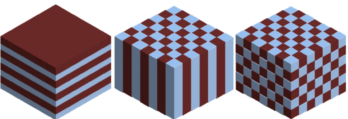
Figure 1-1.3 Phosphor powder of the butterfly with photonic crystal structure.[2] Photonic crystal structures are one kind of the meta-materials that we can obtain the desired optical properties by fabricating the structure with the well-designed geometry. In general, the structure with periodic dielectric distribution can be called photonic crystal structure. There are three kinds of photonic crystal structures divided by the dimension of the periodic dielectrics distribution; those are one-dimensional (1-D), two-dimensional (2-D) and three-dimensional (3-D) photonic crystals. Figure 1-1.4 shows the illustrations of the 1-D, 2-D and 3-D photonic crystals from left to right. Because of the fabrication difficulty, the three dimensional photonic crystals are less realized and discussed compared to the other ones.
Figure 1-1.4 The illustrations of the 1-D, 2-D and 3-Dphotonic crystals from left to right.
4
1-1.2 Photonic Crystal Band Structure
The term of Photonic Crystal has been used after 1987 although it has been studied scientifically for last 100 years. At 1987, Professor Eli Yablonovitch [3] and Saieev John [4] published two papers, which reported the concept of the photonic band gap for the photons in photonic crystal structures. The constructive and destructive interference of light would take place in the photonic crystals. The light with certain wavelength cannot propagate in the structure when the constructive interference regions are not connected. These propagation-forbidden wavelengths form the photonic band gaps. After 1987, the research in photonic crystal increases rapidly. People can control the flow of light by engineering the band structure of the photonic crystals.
In the solid state physics, the motion of the electrons in a crystal will be modulated by the periodic potential function of the nucleuses. A large number of atoms aggregated in a crystal with a specific lattice type will form continuous bands of energy rather than the discrete energy levels of the atoms in isolation. But there are some energy levels that no electrons are allowed to exist with. We call the forbidden regions are the band gaps of the crystal. The behavior of electrons in the crystal can be described with the time-independent Schrodinger equation:
(1.1)
The wavefunction of the electronψ (r) will be influenced by the periodic potential function V(r).
On the other hand, the propagation of the photons in the macrostructure can be affected by the refractive index difference. With the similar concept, the periodic structure with high and low index will form a continuous photonic band of photon
5
energy. Photonic band gaps also exist in the band diagram. The behavior of photons in the photonic crystal can be described with the following equation:
(1.2)
The ɛ(r) is the dielectric constant variation function in space. Given the ɛ(r) to describe the photonic structure, we can solve the equation to get the H(r) for a given frequency. For some frequencies, some solutions are not found. It means the light with the frequency cannot exist in the structure, and the forbidden band is formed.
One-dimensional photonic crystal
One-dimensional photonic crystals consist of alternated dielectric layers with different refractive index. Figure 1-1.5 shows the illustration of a1-D photonic crystal structure. The Figure 1-1.6 (a) shows the lattice of a 1-D photonic crystal structure and (b) the corresponding Brillouin zone. The lattice constant is denoted a. The first Brillouin zone and the irreducible Brillouin zone are formed by the intervals [-π /a, + π /a] and [0, +π /a].
6
Figure 1-1.6 (a) Lattice of a 1-D photonic crystal structure (b) The corresponding Brillouin zone
Figure 1-1.7 is the calculated band structures of 1-D photonic crystal with 13 and 9 alternated dielectric constants and equal thickness. Figure 1-1.8 is the calculated band structures with 13 and 1 dielectric constants. The shadowed regions are the bandgaps of the structures. From the band structures, the band gap size of the 1-D photonic crystal with 13 and 1 dielectric constants are larger than the 13 and 9 one. It implies that the larger index difference of the crystal, the larger band gap size is. In the band structure, the frequency is normalized with the lattice constant. We can obtain the specific modes in the band structure by tuning the lattice constant based on the band diagram. Furthermore, the bandgap size can be controlled by the index difference of the photonic crystal.
Figure 1-1.7 The calculated band structure of 1-D photonic crystal with 13 and 9 dielectric constants. The shadowed region is the bandgap of the structure.
7
Figure 1-1.8 The calculated band structure of 1-D photonic crystal with 13 and 1 dielectric constants. The shadowed region is the bandgap of the structure.
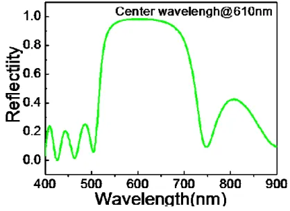
The distributed Bragg reflector (DBR) structure is one of the applications of the 1-D photonic crystal. The light with frequencies in the band gap region acts a total reflected region of DBR. Figure shows the simulation result of DBR. The DBR consist of 6-pair SiO2/TiO2. From the simulation result shown in Figure 1-1.10, the
reflectivity of the wavelength in 550~700 nm approaches perfect because the light on the region is in the photonic band gap of the 1-D photonic crystal. When the white light incident on the DBR structure, the light with frequencies in the bandgap would be reflected and other portion of light would penetrate though the DBR. It can be applied in the solar cells to enhance the quantum efficiency.
8
Figure 1-1.9 Illustration of a DBR structure. The green light would be reflected and other part of white light would pass through the structure.
Figure 1-1.10 Simulation result for the DBR structure. The light with 550 nm~700 nm cannot pass through the structure because it is in the photonic bandgap
9
Two-dimensional photonic crystal
Figure 1-1.11 and 1-1.12 are the illustrations of 2-D photonic crystals. Figure 1-1.11 is the rod structure with higher dielectric constant. Figure 1-1.12 illustrates a high index membrane with some air holes.
Figure 1-1.11 Illustration of two-dimensional photonic crystals of rod structures
Figure 1-1.12 Illustration of two-dimensional photonic crystals of air holes drilled in a membrane.
Here, we take the triangular lattice photonic crystal as an example. The lattice in real space is shown in Figure 1-1.13 (a). Figure 1-1.13 (b) shows the first Brillouin zone (colored region), which is a smallest enclosed region in reciprocal space formed by the bisectors of the lattice vectors nearby the origin. Figure 1-1.13 (c) shows the irreduced Brillouin zone of triangular lattices (colored region). The symmetry points are denoted “Г, M and K”
10
Figure 1-1.13 (a) Illustration of triangular lattice two-dimensional photonic crystals (b) The first brillouin zone (colored region) (c) The irreduced Brillouin zone
of triangular lattices (colored region).
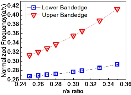
The band structure of the 2-D photonic crystal triangular lattice in a suspend membrane structure is shown in Figure 1-1.14. The 3-D plane-wave extension method was used to calculated the band structure of the photonic crystals with 0.3 radius to lattice constant ratio (r/a) and 430 nm lattice constant. The modes above the light line would be leakage modes. All possible states propagate in the air; therefore, we block the regions above the light line with black color in the band structure. Below the light line, the modes are confined to the slab. The first band gap is at the 0.272 to 0.338 normalized frequency. As the r/a ratio is increased, all of the optical modes will shift to higher frequency region. The blue-shift speeds of different optical modes are not identical. Figure 1-1.15 shows that the normalized frequencies of the first band-edges can be changed by varying the r/a ratio. We find that the first bandgap size is also different with different r/a ratio.
11
Figure 1-1.14 The band structure for TE modes of a 2-D triangular lattice photonic crystal with 0.3 r/a
Figure 1-1.15 The normalized frequencies of the first band-edges can be changed by varying the r/a ratio.
12
1-1-3 Photonic Crystal Lasers
The photonic crystal structure is widely used in the applications such as to improve the light extraction efficiency of LED [5], photonic crystal waveguide [6] and so on. One of the important applications of photonic crystals is the photonic crystal lasers. A laser consists of a gain material in a resonate cavity. The light goes through the gain material and the energy of light is then amplified. The process of supplying energy for the amplification is pumping. As for the photonic crystal lasers, the structures are always fabricated with high refractive index gain material. The photonic crystals form a resonate cavity for specific wavelengths. The lasing action would be observed when the threshold condition is reached by the optical or electrical pumping.
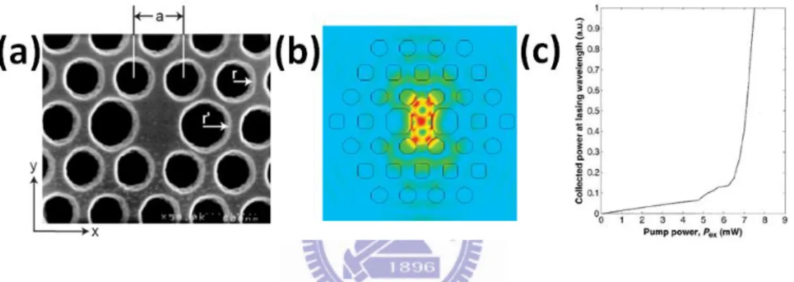
In recent years, two-dimensional photonic crystals have become popular due to fabrication improvements and the applications of photonic crystal lasers. In 1994, the idea was proposed by using photonic crystal as resonator. In 1999, the first photonic crystal lasers were demonstrated. Generally speaking, the photonic crystal lasers can be divided into two categories, photonic crystal defect lasers and photonic band-edge lasers. We can create a defect by removing some air holes off or fine tune some air hole positions in the photonic crystals. Light with the forbidden frequency of the photonic band structure will localized and resonate in the defect region. The light will resonate in the plane by the effect of photonic crystal and vertically confined by the large index difference. Once the gain overcomes the loss, the lasing action will be observed. Figure 1-1.16 shows the two mechanisms of the light confinement of a 2-D photonic crystal defect laser. This was first demonstrated by the group of O. Painter [7]. The 2-D photonic band gap and vertical index guiding provide a low loss resonance cavity of the laser. Figure 1-1.17 shows one of examples of a defect laser. The light resonates in the defect region and achieved lasing. The mode profile of the lasing mode is also shown in the Figure 1-1.17 (b).
13
Figure 1-1.16 The configuration of the two-dimensional photonic crystal defect laser[7]
Figure 1-1.17 (a) The SEM image of the defect region. (b)The simulated mode profile distribution of the lasing mode. (c) The light-in light-out curve of the defect laser.[7] The modes of the deferent kinds of defect lasers and the different modes in the same kinds of the defect laser would all have different optical properties. People can investigate the modes and pick up some desired modes with some specific polarization or lasing wavelength.
On the other hand, the photonic crystal band-edge laser has no physical-defined cavities. They utilize the flat band near the band edge in the photonic band diagram. The group velocity of light approaches zero there and the lasing action is expected. There is one band-edge laser shown in Figure1-1.18 [8]. The triangular lattice photonic crystal without any defect can achieve lasing, which is shown in the Figure 1-1.19(a). Compared with the simulation, the lasing modes are at the Г symmetry points, which is denoted as A and B in Figure 1-1.19 (b). The calculated band structure is also shown in the Figure 1-1.19 (b).
14
Figure 1-1.18 The configuration of a photonic crystal band-edge laser [8]
Figure 1-1.19 (a) The lasing spectrum and (b) Band structure of the photonic crystal band-edge laser. [8]
15
1-2 Motivation and Overview of Thesis
Photonic crystal lasers attract a lot of attention these years. The size is very small compared with other kinds of lasers such as gas lasers. It can be applied in the dense photonic integrated circuit as a signal source [7]. On the other hand, the goal to design and fabricate the thresholdless laser is another important issue of the photonic crystal laser. We can obtain the laser light with less energy input by the small threshold power photonic crystal lasers.
However, for this kind of semiconductor lasers, the lasing wavelength cannot be altered easily because the lasing wavelength strongly depends on the laser geometry. It limits lots of application due to the single-wavelength property. From another point of view, the change of geometry in the macro-scale area can be detected by the difference in the lasing wavelength. We can measure the wavelength variation to get the information of the local structure deformation instead of using SEM or other more complex methods.
On the other hand, the polymer and organic devices has been studied widely because the application flexibilities. There are demonstrations in the flexible platform for the light source [9-14], modulators [15-16] and sensors [17-18]. Our goal is to integrate the compactness and flexibility. In this way, the application flexibility of the semiconductor devices will increase largely with a compact size.
In this thesis, we demonstrate the multi-wavelength photonic crystal band-edge laser with a flexible PDMS substrate. The optical properties of the lasing modes will changed when the structure is bent. For different lasing modes of the laser, the response to the bent structure will be different. Furthermore, we perform simulations to the phenomenon. Compared with the simulation result, we can deduce the possible geometry variation of the bent laser and estimate the variation percentage for different bending curvature. In this way, we can characterize this flexible photonic crystal laser system.
16
With the flexible laser technology, we can fabricate a single device to get a multi-wavelength photonic crystal laser instead of fabricating lots of photonic crystal devices with different lattice constants. Then, the cost of the multi-wavelength device will be reduced. The application in optical communication will be practicable.
17
Chapter 2 Fabrication Procedures
In this chapter, the fabrication instruments will be introduced. We will show how to fabricate the photonic crystal lasers on a PDMS substrate. The preparation of the PDMS substrate will also be introduced in the following content.
2-1 Introduction to the Fabrication Instruments
2-1-1 The Scanning Electron Microscope (SEM) System
For the micro-scale photonic crystal devices, it is important to check the geometry parameters in the fabrication process. We can not only assure whether the device is successfully fabricated but also can perform the simulations with these parameters to further understand the data we recorded. The scanning electron microscope is the key instrument for the macro fabrication process. It acts as the eyes for us to check the device step by step in the process flow. Figure 2-1.1 shows the scanning electron microscope system. The system model is Inspect F from FEI Company.
18
Figure 2-1.1 Picture of the scanning electron microscope system
2-1-2 Plasma Enhanced Chemical Vapor Deposition(PECVD) System
We have to deposit silicon nitride (SiNx) layer as a hard mask layer on the
epitaxial wafer for the following fabrication process. We use the Oxford plasmalab 80 plus to deposit 240 nm thickness SiNx on the epitaxial wafer with SiH4/NH3/N2
mixture gases. The SiNx thin film quality strongly depends on the NH3/ SiH4gas ratio.
The SiNx thin film deposited with NH3 addition would be easy for chemical etching
process. Actually, the SiNx layer can also be deposited at absence of NH3 gas. In this
way, the resistance to InP dry etching will be much higher, but the SiNx layer cannot
be removed completely by the BOE wet etching. It is a trade off because the high resistance to dry etching is good for the InP etching but it is hard for the pattern on PMMA to be transferred to SiNx layer. As a result, we tried different recipes by
changing NH3/ SiH4 ratio and find the acceptable recipe for the fabrication procedures.
Finally, the equal amount of NH3 and SiH4 gases is used for the SiNx deposition. We
deposit SiNx layer with 8 sccm SiH4, 8 sccm NH3, 250 sccm N2. The RF power is 20 w,
19
Figure 2-1.2 Picture of the plasma enhanced chemical vapor deposition system
2-1-3 E-beam Lithography Process
Because the patterns are in macro scale, the electron-beam lithography is used instead of traditional optical lithography method. We use the polymethylmethacrylate (PMMA) as the e-beam resist. The PMMA is a standard positive electron beam resists with 950,000 molecular weight resins in chlorobenzene either anisole. The ratio of PMMA to the anisole is 5:100, which is called A5. The more the PMMA dissolve into anisole the bigger thickness for the same spin speed of coating.
We spin coat the PMMA on the top of the SiNx-deposited wafer by a spin coater
with two steps. The rotation speed is 1000 revolution per minute (rpm) for ten seconds in first step. The PMMA would be uniform on the wafer after step 1. The step 2 starts instantly with 3500 rpm for 3 minutes to get the thinner thickness. After coating the PMMA, some of the solvent will vaporize by the 180 ̊C baking for 2 minutes. The PMMA would be harder after backing. The thickness of the PMMA would be around 300 nm after these steps.
20
We use the e-beam lithography process to define the patterns with PMMA on the SiNx deposited wafer. After e-beam exposure, the exposed area would be developed
with a mixture solution of isopropanol (IPA) and MIBK with 3:1 ratio for 70 seconds. The ratio of MIBK and isopropanol affects the resolution and sensitivity. The lower MIBK to IPA ratio is, the higher resolution is; but the sensitivity is lower. After the develop process, we use the pure isopropanol to remove the developer, and immerse the sample in deionized water. Finally, we dry the sample by nitrogen gas.
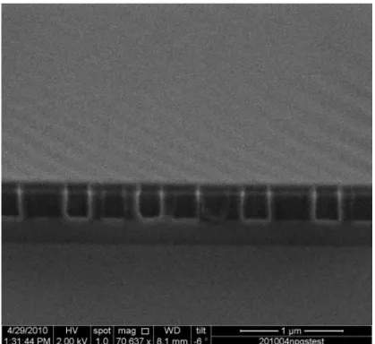
We can check whether the patterns are successfully developed by OM system. Figure 2-1.3 shows a SEM image of the cross section view to the air hole patterns after the develop process. The vertical profile of the hole shapes indicates that the e-beam dosage is appropriate for the pattern and the develop process is successful.
21
2-1-4 ICP/RIE System
In the fabrication procedures, the patterns on PMMA are transferred to the SiNx
and further to InGaAsP layer by dry etching process. The anisotropic etching of dry etching is very common in the semiconductor industry. The key process of the dry etching is the plasma formation. The plasma is a state of matter similar as gases in which part of the particles are ionized. With the well selection of gas types, the active plasma would react with the exposed area and forms the gas-type products which would be pumped out of the system. This kind of reaction is chemical etching process. Sometimes we need some high weight ions to bombard the reactant surface in order to increase the etching rate. Combination of sputtering and chemical etching processes significantly increases etching rate in a specific direction. It may caused by the higher local temperature of the bombardment area to increase the chemical etching rate. This kind of the etching is called reactive ion etch (RIE) process. If we want to increase the plasma density, we can make the electrons accelerated in angular direction. The RF power is inductivity couples to plasmas, which is called inductive couple plasma (ICP). In this way, we can achieve high plasma density at low temperature. Besides, it allows independent control of ion flux and ion energy, which is feasible for us to control the etching condition.
Our dry etching system is ICP/RIE system. The brand model is Oxford Plasmalab system 100. CHF3, O2, N2 and Cl2 are provided for dry etching. We can
tune recipes by varying the gas flow, chamber pressure, temperature, RF power and ICP power. The high density plasmas of this system are very useful for fabricating the sub-micron structures with controllable selectivity, sooth morphology, vertical profile and high etching rate.
22
Figure 2-1.4 Picture of the ICP/RIE System
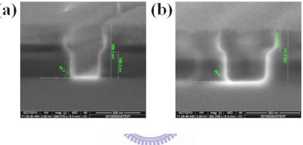
The defined patterns are transferred to SiNx layer by RIE at 20℃with CHF3:50
(sccm), O2:5 (sccm), RF power:150 (W) and pressure:55 (mtorr). Figure 2-1.5 and
Figure 2-1.6 shows the SiNx etching profile the line with 200 nm line width and holes
with 200 nm in diameter. The vertical profile is obtained by controlling the etching time. After removing the residual PMMA, the pattern was transferred into the InGaAsP MQWs layers by ICP etching at 160℃ with N2:6 (sccm), Cl2:5 (sccm), RF
power:100(W) , ICP power:400(W) and pressure: 10 mtorr. Figure 2-1.7 shows the InP etching profile of the line with 200 nm line width and holes with 200 nm in diameter. The selectivity is about 9 for the photonic crystal patterns.
23
Figure 2-1.5 Cross section view of SiNx etching profiles.
Figure 2-1.6 Cross section view of SiNx etching profiles (a) line with 200 nm
linewidth (b) holes with 200 nm in diameter.
Figure 2-1.7 Cross section view of InP etching profiles (a) line with 200 nm linewidth (b) holes with 200 nm in diameter.
24
2-1-5 Wafer Bonding to PDMS Substrate
A commercial polydimethylsiloxane (PDMS) material (Sylgard 184, supplied by Dow Corning) serves as a flexible polymer here. PDMS is optically clear and considered to be inert, non-toxic and non-flammable. It acts as an elastic solid, similar to rubber. The PDMS substrate is prepared by mixing the Sylgard184A and Sylgard184B solutions with a 4:1 ratio of volumes. As the ratio becomes larger, the PDMS will be softer. That is to say, the ratio of the A and B solutions determines the hardness of the PDMS substrate. It takes about 1day that the mixed solution can be stiffening at 25℃. The PDMS thickness is controlled by the volume of the PDMS glue we added. The refractive index of the PDMS is about 1.43, which can support good light confinement in the vertical laser structure.
The InP-etched devices can be put upside down and bonded directly on a well-prepared PDMS substrate. After we bonding the device to the PDMS substrate, the InP substrate will be removed by dilute HCl solutions (HCl: H2O=3:1) at room
temperature for 40 minutes. The PDMS can afford strong acid and base; therefore it would not be destroyed in the wet etching process.
25
2-2 Fabrication Steps for Flexible Photonic Crystal
Laser
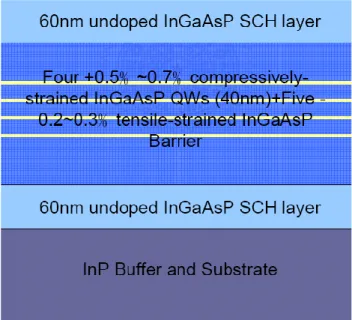
The triangular-lattice photonic crystal structures are fabricated on a polydimethylsiloxane (PDMS) substrate. The illustration of the laser structure is shown in Figure 2-2.1. The 240 nm thick InGaAsP active layer consisted of four 10-nm-thick strained InGaAsP quantum wells (QWs). The epitaxial structure of InGaAsP/InP MQWs for the device is shown in Figure 2-2.2. It has been confirmed that the photo-luminance spectrum (PL) of the QWs is centered at 1550 nm and the full-width half-maximum (FWHM) is about 200 nm. The PL spectrum is shown in Figure 2-2.3
Figure 2-2.1 Illustration of the triangular lattice photonic crystals on a PDMS substrate.
26
Figure 2-2.2 The epitaxial structure of InGaAsP QWs
Figure 2-2.3 The PL spectrum of InGaAsP/InP MQWs
The PDMS substrate with a 500 um thickness was served as a flexible platform here. The refractive index of the PDMS was about 1.43, which was low enough to support good optical confinement in the vertical direction of the lasers.
There are seven steps to fabricate the flexible devices. First, we deposited silicon-nitride (SiNx) on the epitaxial wafer as a hard mask, and spin-coated
27
crystals were patterned on PMMA by electron-beam lithography. The lattice constant varied from 370 nm to 430 nm. Followed by RIE and ICP dry-etching processes, we transferred the patterns to the SiNx layer with CHF3/O2 mixture gases at 20℃ and
further to the QWs layer with N2/H2 mixture gases at 160℃. After that, we bonded the
QWs layer to the well-prepared PDMS substrate. Finally, the photonic crystal structure on the PDMS substrate was obtained by selective wet etching with the HCl diluted solution to remove the InP substrate. Figure 2-2.4 is the picture of the fabricated structure on a PDMS substrate. Figure 2-2.5 shows the scanning electron microscope (SEM) image of a fabricated triangular-lattice photonic crystal band-edge laser on a PDMS substrate.
Figure 2-2.4 Picture of the fabricated structure on a PDMS substrate
28
The fabrication flow chart is shown below step by step.
SiNx deposition with PECVD system
PMMA spin-coating on the SiNx hard mask
Pattern defined with the electron-beam lithography system
Step1
Step2
29
Pattern transferred to SiNx layer with ICP/RIE
etching
Pattern transferred to InGaAsP layer with ICP/RIE etching
Bonding the structure upside-down on the PDMS substrate
Step4
Step5
30
HCl wet etching to remove the InP substrate.
Finally, we get the fabricated devices.
2-3 Conclusion
In conclusion, we introduce the fabrication procedures for the photonic crystal lasers on a flexible PDMS substrate. Then, we introduce the fabrication instruments and the recipes we used. With the well-tuned recipe, the devices are successfully fabricated and the SEM image of the device is also shown in this chapter.
31
Chapter 3 Measurement Result
In this chapter, the measurement results of the fabricated devices will be shown. The lasing modes would be confirmed by the measurement result of the different lattice constant devices. We also bend the laser structure to measure the optical properties with different bending curvatures.
3-1 The Micro-PL Measurement System
In order to measure the optical properties of the photonic crystal micro-cavities, the micro-PL measurement system with sub-micrometer scale resolution in space and sub-nanometer scale resolution in spectrum is necessary. Figure 3-1.1 shows the micro-PL measurement system.
32
In the measurement system, the 850 nm diode laser is used as the pump source. The pump power is modulated by the amplitude modulator. The laser light goes through the 50/50 beam splitter, 50% of pump power is reflected into the photo-detector to know how much pump power that is used and the other 50% pump power is focused to a spot with 1.5 um to 2 um in diameter by the 100x NIR objective lens. The sample is mounted on a high resolution motor control 3-axis stage with 30 nm move resolution. The output power was collected from the top of the sample into the optical spectrum analyzer (OSA) by the objective lens, collective lens and multi-mode fiber. Because the most of the photonic crystal devices are only few um or sub-um scale, here we have to use the visible light system to observe the position of the pump spot and devices. The visible light system includes the visible light sources, CCD camera and monitor.
33
3-2 Lasing Characterization with a Flat PDMS
Substrate
We fabricated arrays of photonic crystal triangular lattices on a PDMS substrate. One of the fabricated arrays of photonic crystal patterns is shown in Figure 3-2.1. The SEM image shows there are thirty-five patterns in an array. The lattice constants varied from 345 nm to 515 nm. Figure 3-2.2 shows the photonic crystal triangular lattices on a PDMS substrate with 410nm lattice constant. There are about thirty periods of the lattice in both Г-K and Г-M directions.
Figure 3-2.1 The SEM image of the array of patterns with different lattice constants
Figure 3-2.2 The SEM image of the photonic crystals with 410 nm lattice constant
34
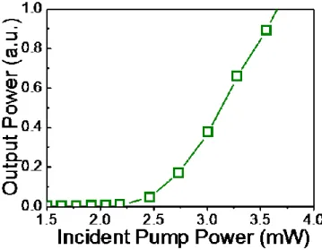
Figure 3-2.3 shows the lasing spectrum from the triangular lattice photonic crystal band-edge laser with 395 nm lattices constant. The lasing wavelength is about 1581 nm. The side mode suppression ration is about 18 db, which is high enough for optical communication. The light in-light out curve (L-L curve) from the laser is show in Figure 3-2.4. The threshold power is about 3.2 mW. It is higher than the threshold power of photonic crystal defect lasers. The mode volume of the photonic crystal band-edge laser is larger than other defect lasers; therefore it needs higher power to achieve lasing.
Figure 3-2.3 The lasing spectrum from the photonic crystal band-edge laser with 395 nm lattice constant
Figure 3-2.4 The light in light out curve from the 395 nm lattice constant photonic crystal band-edge laser
35
In order to characterize the operation mode of the photonic crystal band-edge laser, we measured the photonic crystal band-edge lasers with different lattice constant in the same array of patterns. The photonic crystals with different lattice constant in the array would have the same r/a ratio. Figure 3-2.5 shows the lattice constant versus the lasing wavelength. As the lattice constant increases, the lasing wavelength increases linearly. It indicates that these lasing modes are the same mode with 0.249 normalized frequency.
Figure 3-2.5 The lasing wavelength versus lattice constant of photonic crystal band-edge lasers on a PDMS substrate. The normalized frequency of the lasing mode
is about 0.249.
We also find out other operation modes of the photonic crystal band-edge laser. Figure 3-2.6 is the lasing spectrum measured from 430 lattice constant triangular lattice photonic crystal band-edge laser. The lasing wavelength is about 1627 nm. Figure 3-2.7 is the L-L curve from the laser. The threshold power is approximately 2.7 mW.
36
Figure 3-2.6 The lasing spectrum from the photonic crystal band-edge laser with 430 nm lattice constant.
Figure 3-2.7 The light in light out curve from the 430 nm lattice constant photonic crystal band-edge laser
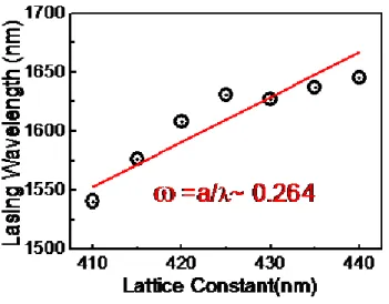
By measuring the lasers with lattice constant around 430 nm, we can get the relationship between the lasing wavelength and lattice constant and identify the lasing mode. Figure 3-2.8 shows the lasing wavelength versus lattice constant. The normalized frequency of the mode is about 0.264.
37
Figure 3-2.8 The lasing wavelength versus the lattice constant. The normalized frequency of the operation mode is about 0.264.
38
3-3 Optical Properties of the Bent Photonic Crystal
Laser
After characterizing the operation modes of the photonic crystal band-edge laser with a flat PDMS substrate, we measure the bending structure on a bent mental surface. Figure 3-3.1 illustrates the bent triangular lattice photonic crystal band-edge laser with bending radius R. We bend the structure long the Г-M direction of the triangular lattice. Figure 3-3.2 shows our handmade tool for controlling the bending curvature (1/R). We can increase the bending curvature by rotating the micrometer. The micrometer would pull the mental slice in and make the mental slice bent. We call the distance that the micrometer pulled in bending depth. For example, the distance between two red lines in Figure 3-3.3 is the bending depth, and the mental slice is bent by rotating the micrometer. Then, we derivate the value of bending curvature from the geometry of the bending tool. Figure 3-3.4 shows the relationship between bending depth and bending curvature.
39
Figure 3-3.2 The measurement tools for bending the structure. The upper is a mental slice, which is served as a bending platform here. The lower is a homemade
tool with a micrometer. A flat mental slice is equipped.
Figure 3-3.3 The bending measurement tools with a bent metal slice. The distance between the two red lines is the bending depth.
40
Figure 3-3.4 Bending depth versus bending curvature.
In the measurement, we apply the device on the varying bent mental surface with fixed pump condition and pump position. At first, we measure the PL spectrum of the MQWs with different bending curvatures. Figure 3-3.5 is the PL spectrums of the MQWs with different bending curvatures. The PL spectrums do not shift when the bending curvature is increased.
41
We measure the 395 nm lattice constant triangular lattice photonic crystal laser with the lasing mode of 0.249 normalized frequency. Figure 3-3.6 shows the light in light out curve of the laser with different bending curvature. The structure does achieve lasing at varied bending curvature. From the Figure 3-3.7, we can find out that as the bending curvature increases, the threshold power increases. Figure 3-3.8 shows that the output power decreases as the bending curvature increases. When the curvature is increased to 0.06 (1/mm), an increase of 20% in threshold power and a drop of 70% in output power are observed. These behaviors are attributed to the increase of optical loss due to the structure deformation. The output power drops more rapidly than the increase of the threshold power because we do not collect the entire laser light due to larger divergent angle of the bent laser. In other words, we only collect small part of the laser light in our OSA when the laser structure is bent.
Figure 3-3.6 The light in light out curve of the 395 nm photonic crystal band-edge laser with different bending curvature.
42
Figure 3-3.7 The threshold power versus the bending curvature of the 395 nm photonic crystal band-edge laser
Figure 3-3.8 The output power versus the bending curvature of the 395 nm photonic crystal band-edge laser
The lasing wavelength is another important optical property. After bending the structure, we observe the lasing wavelength red-shifts. Figure 3-3.9 shows the lasing wavelength red-shifts as the bending curvature is increased.
43
Figure 3-3.9 The lasing wavelength versus the bending curvature of the 395 nm photonic crystal band-edge laser
The lasing wavelength red-shifts when the structure is bent. It implies that it can be applied as a wavelength tunable laser light source in optical communication. The cost of the semiconductor laser is high; once the structure is defined, the lasing wavelength would hard to be altered. It means if we want a multi-wavelength light source, we must fabricate many devices and fine tune their geometry parameter. Here, we demonstrate the multi-wavelength light source in a single device by bending the structure; therefore, the cost for the multi-wavelength light source becomes lower. Besides, the flexible laser can be a local curvature sensor with a very compact size. Base on the experiment result, the sensibility is about 29 nm/mm-1.
We also measure the photonic crystal band-edge laser with 430 nm lattice constant. The normalized frequency of the lasing mode is 0.264, which is shown beforehand. Figure 3-3.10 shows the light in light out curve of the 430 nm lattice constant photonic crystal laser with different bending curvature. The structure achieves lasing at varied bending curvature. Figure 3-3.11 is the threshold power versus the bending curvature. The threshold power increases as the bending curvature, too.
44
Figure 3-3.10 The light in light out curve of the 430 nm lattice constant photonic crystal laser with different bending curvature.
Figure 3-3.11 The threshold power versus the bending curvature of the 430 nm lattice constant photonic crystal laser
Figure 3-3.12 The lasing wavelength red-shifts as the curvature is increased. Compared with the previous optical mode of 0.249 normalized frequency, the red-shifts of this mode is about 40% less than the previous mode at the same bending curvature.
45
Figure 3-3.12 The lasing wavelength red-shifts as the curvature is increased of the 430 nm lattice constant photonic crystal laser
3-4 Conclusion
In this chapter, we demonstrate the triangular lattice photonic crystal lasers on a flexible PDMS substrate. The lasing actions of the lasers are observed with different lattice constant and the two lasing modes of 0.249 and 0.264 normalized frequencies are identified. The optical properties of the lasers with different bending curvature are also shown in this chapter
46
Chapter 4 Simulation Result and Analysis
In this chapter, the plane wave expansion (PWE) method is introduced. We calculate the band structures with 3-D plane-wave expansion method. Then, the model of the geometry deviation on a bent structure is brought up. After that, we estimate the lattice extend percentage by comparing the simulation and measurement results.
4-1 Plane-Wave Expansion (PWE) Method
We use the plane-wave expansion method to calculate the band structures of the photonic crystals. The plane-wave expansion method will be introduced first.
The behavior of the electromagnetic waves can be described by the following Maxwell equations:
0,
0
,
B
B
E
t
D
D
H
J
t
(4.1)Where B and D are the displacement and magnetic induction field, E and H are electric and magnetic field, and ρ and J are free charge and current density. We assume the system is source free medium ( ρ = 0 ) and nonmagnetic materials ( μ = 1 ). Then the Maxwell’s equations become:
0( ) ( , )
r E r t
0
(4.2)
0( )
r H r t
( , )
0
47 0
( , )
( , )
E r t
H r t
t
(4.4) 0( , )
( )
( , )
H r t
r
E r t
t
(4.5) Where r is direction vector and t is time.Then we take the both equation 4.4 and equation 4.5 for curls and the equation 4.5 is divided by ( )r on both sides, then we get equations 4.6 and 4.7:
0
[
E r t
( , )]
[
H r t
( , )]
t
(4.6) 01
[
( , )]
[
( , )]
( )
r
H r t
t
E r t
(4.7)Next replace these two term s
E r t
( , )
and
H r t
( , )
in equation 4.6 and 4.7 by equation 4.4 and 4.5 respectively, and we get 4.8 and 4.92 0 0 2
[
E r t
( , )]
( )
r
E r t
( , )
t
(4.8) 2 0 0 21
[
( , )]
( , )
( )
r
H r t
t
H r t
(4.9)For mathematics convenient, we introduce the complex forms of E and H
( , )
( )
tE r t
E r e
(4.10)( , )
( )
t48
then replace 4.8 and 4.9 by 4.10 and 4.11, furthermore, we express light velocity
0 0
1 c
, then equation 4.8 and 4.9 become:
)
(
)
(
)]
(
)
(
1
[
2E
r
c
r
E
r
(4.12))
(
)
(
)]
(
)
(
1
[
2H
r
c
r
H
r
(4.13)Where 2 is eigenvalue. Then replace
1 ( ) ( ) E r and 1 ( ) ( ) H r
to both equations, we get:
2
( )
( )
( )
EE r
E r
c
(4.14) 2( )
( )
( )
EH r
H r
c
(4.15) From equations 4.14 and 4.15, the operator in this equation is Hermitian operator. It implies eigenvalues (or frequency) are real and the eigenvectors (or harmonic mode) are orthogonal to each other with different eigenvalues. In addition, another property is scaling properties. Because master equation is scaling invariant, there is no fundamental constant with the dimensions of length for photonic crystal.There are several ways to calculate photonic band structure. The most common way is plane wave expansion method. Consider equations 4.14 and 4.15:
2
( )
( )
( )
EE r
E r
c
(4.14)49 2
( )
( )
( )
EH r
H r
c
(4.15) ( )r is periodic function of the photonic crystals, so that ( )r can be expressed by
the Fourier’s series
1
( )
( )
iG r GG e
r
(4.16)According to Bloch’s theorem, with periodic structure, wave function must be expressed as a plane wave times a function with the periodicity of the Bravais lattice:
( )
( )
i k rk
r
kr e
(4.17)
Where the k(rR)k( )r
So the E r( ) and H r( ) can be expressed as:
( )
k( )
i k rE r
u r e
(4.18)( )
k( )
i k rH r
s r e
(4.19)Where the u rk( )u rk( R) and s rk( )s rk( R)
Applying equation 4.17, 4.18 and 4.19 to equation 4.14 and 4.15, we can get the following equation: ' ' ' ' ' 2 '
(
)(
) {(
)
k(
)}
k k(
)
GG
G
K
G
K
G
E G
E G
(4.20)50 ' ' ' ' ' 2 '
(
)(
) {(
)
k(
)}
k k(
)
GG
G
K
G
K
G
H G
H G
(4.21)Solve these two equations numerically, and plot the dispersion relation of
and k to get the photonic band structure.
In this thesis, all the band structure calculations are performed with PWE method by the commercial software R-soft.
51
4-2 Optical Modes of the Band-edge Lasers
In order to investigate the optical modes of the triangular lattice photonic crystal lasers on a flexible PDMS substrate, we calculate the corresponding band structure of the photonic crystal by 3-D plane-wave expansion (PWE) method for TE-like modes. Figure 4-2.1 is the calculated band structure with 0.25 radius to lattice constant ratio. Compared with the suspend membrane structure, the light core shifts to the lower frequency region because the PDMS substrate has higher refractive index than air. The band-edge lasing modes are likely to occur around the high-symmetry points of the band structure. The flat dispersion curve near the band-edge implies a low group velocity of light and strong localization. Hence, the light-matter interaction can be enhanced and lasing action is expected. Figure 4-2.2 shows the group velocity of light with different in-plane wave vector k of Г to M point. At the symmetry point M, the group velocity approaches zero and the lasing action is expected.
At chapter 3, we have measured two lasing modes with the normalized frequencies around 0.249 and 0.264. Comparing the measurement with simulation, we identify the M1 and the K1 in the band structure are the operation modes of the
photonic crystal lasers.
Figure 4-2.1 The TE-like mode band structure of the triangular lattice photonic crystals with 3-D plane-wave expansion method. The K1 and M1 are identified as the
52
Figure 4-2.2 The group velocity versus different wave vector k. The group velocity approaches zero for modes near the M1.
53
4-3 Model for Geometry Variation in the Flexible
Photonic Crystal Laser System
In the experiment, we observed that the lasing wavelength of the band-edge laser red-shifts as the bending curvature is increased. Here, we attribute the red-shift to the lattice distortion and the change of the PDMS refractive index.
The lasing wavelength of the photonic crystal lasers strongly depends on the laser geometry. We can modify the lattice constant to make the device achieve lasing at specific wavelength. In this flexible laser system, as we bend the structure along Г-M direction, the red-shifts in lasing wavelength are observed. These red-shifts imply that the geometry of the laser would be changed when the structure is bent. In other words, we can measure the change in lasing wavelength to presume the possible mechanism of the geometry variation. By comparing the measurement with the simulation, we can quantize the geometry variation in the flexible laser system. We create a model for the geometry variation in the flexible laser system. Figure 4-3.1 and Figure 4-3.2 illustrate the photonic crystals on a plate and on a bent PDMS substrate relatively. We assume that the lattice constant in the Г-K direction will increase as the structure is bent; the lattice constant in the Г-M direction would remain the same. Figure 4-3.3 shows the triangular lattice photonic crystals and the Г-K and Г-M directions.
54
Figure 4-3.1 The illustration of the triangular lattice photonic crystals with a plate PDMS substrate.
Figure 4-3.2 The illustration of the triangular lattice photonic crystals with a bent PDMS substrate.
Figure 4-3.3 The illustration of the triangular lattice and the Г-K and Г-M directions of the lattice.
55
On the other hand, the refractive index of the PDMS substrate will become smaller when the structure is bent. We assume that the volume of the PDMS substrate will increase as the curvature is increased. With the equation 4.22[19], we can obtain the PDMS refractive index at different curvatures by estimate the enlarge volume of the PDMS substrate.
(4.22)
The symbol V in equation 4.22 is denoted as the volume of the PDMS substrate. Because the negative sign in the equation, the PDMS index will become smaller when the PDMS volume is increased. Figure 4-3.4 shows the refractive index of the PDMS substrate versus the bending curvature.
Figure 4-3.4 The refractive index of the PDMS substrate versus the bending curvature.
56