對應低溫多晶矽薄膜電晶體變動性之電路模擬技術之研究
66
0
0
全文
(2) 對應低溫多晶矽薄膜電晶體變動性之 電路模擬技術之研究 Study on the Circuit Simulation Techniques Corresponding to the Variation of LTPS TFTs 研 究 生:陳琬萍. Student : Wan-Ping Chen. 指導教授:戴亞翔 博士. Advisor : Dr. Ya-Hsiang Tai. 國 立 交 通 大 學 光電工程學系 顯示科技研究所 碩 士 論 文 A Thesis Submitted to Department of Photonics Display Institute College of Electrical Engineering and Computer Science National Chiao Tung University in Partial Fulfillment of the Requirements for the Degree of Master in Display July 2006 Hsinchu, Taiwan, Republic of China. 中 華 民 國 九 十 五 年 七 月.
(3) 對應低溫多晶矽薄膜電晶體變動性之電路模擬技術之研究 研究生:陳琬萍. 指導教授: 戴亞翔 博士. 國立交通大學光電工程學系顯示科技研究所. 中. 文. 摘. 要. 雷射再結晶的低溫多晶矽薄膜電晶體(LTPS TFT)廣泛應用在主動式矩陣的顯示器 (active matrix display)及其驅動電路,因而備受矚目。在本篇論文,首先將統計性研究探 討低溫多晶矽薄膜電晶體(LTPS TFT)變動性之特性,並提出二種適當描述變動性的非高 斯函數式,其正確性指標高達 0.9。 根據提出的函數式,建立一個考慮元件參數變異的新描述模式,並將其應用在電路 模擬,以差動對與環形震盪器為例,比較其電路中元件參數用新提出方法與傳統高斯分 配所產生後模擬電路的輸出結果。模擬結果顯示出,用提出的新方法模擬電路與實際量 測到的元件參數直接帶入模擬的結果非常相像,這足以反應所提出模式的正確性。 根據模擬結果,如同環形震盪器之類的數位電路,其電路成效主要受區域的變動性 所主導。相反地,如同差動對之類的類比電路,其電路成效主要受微小範圍的變動性 (micro variation)所影響。. i.
(4) Study on the Circuit Simulation Techniques Corresponding to the Variation of LTPS TFTs Student : Wan-Ping Chen. Advisor : Ya-Hsiang Tai. Department of Photonics & Display Institute National Chiao Tung University. Abstract. Laser recrystallized low temperature poly-silicon (LTPS) films have attracted attention for their applications in thin-film transistors (TFTs), which are widely used in active matrix displays and its driving circuits. In this thesis, the variation characteristics of LTPS TFTs are statistically investigated. Two kinds of non-Gaussian equations are proposed to fit the variation behaviors, which the coefficients of determination are both near 0.9, reflecting the validity of the model. Based on the proposed model, a new description of device parameter considering variation is provided and is applied in circuit simulation. Taking the differential pair and ring oscillator as the benchmarks, the proposed method of device parameter generation are compared with the conventional Gaussian distribution with the output performance of the circuit. It can be seen that the performance of the proposed model behaves much like those parameters from the measured device parameter, which reflects the validity of the proposed model. According to the simulation results, the circuit performance of a digital circuit, such as ring oscillator, is dominated by the variation in the range. On the contrary, the circuit performance of an analog circuit, such as differential pair is dominated by micro variation of devices. ii.
(5) 誌. 謝. 首先我要感謝我的指導教授戴亞翔博士,總是鼓舞、激發我們,耐心用 心地指導我們。除了研究學習,老師也會跟我們分享生活上做人處事的道 理,讓我受益良多。在此,對我敬愛的戴老師致上最誠摯的謝意。 感謝,士哲學長、宏光學長、承丘學長、承和學長、彥甫學長與大山學 長,謝謝你們適時地解決我許多課業上的問題,也給我精神上的鼓勵。 感謝,實驗室的同學們,彥邦、可青、皓麟、鈺函、建焜、國烽,以及 富智,這段一起奮鬥、一起討論、互相打氣的日子,都是難忘的美好回憶。 感謝,實驗室的學弟妹們,育德、晉煒、俊文、虹娟、偉倫、振業、曉 嫻、長龍,以及明憲,謝謝你們的關心與協助。 感謝,我親愛的家人們,還有怡慧、雅婷、小豆、黃恆,以及所有好友 們,感謝你們一直以來的陪伴、支持與關懷。 最後感謝口試委員張鼎張教授、劉柏村博士、楊士禮博士在口試時給予 相關的建議與指導。 琬萍 2006.07.31. iii.
(6) Contents Chinese Abstract ………………………………………………………………………. i English Abstract ………………………………………………...……………………. ii Acknowledgements ……………………………………………….......……………... iii Contents …………………………………………………………..……………………. iv Figure Captions ………………………………………………………………………. vi Table Captions ………………………………………………………………………. viii Chapter 1. Introduction. 1.1 LTPS TFT …………………………………………………………………………... 1 1.2 Device Variation ……………………………………………………………………. 2 1.3 Motivation ………………………………………………………………………….. 3 1.4 Thesis Outline …………………………………………………………………….... 4. Chapter 2. Statistical Descriptions of Device Variation. 2.1 Introduction to Crosstie TFTs ……………………………………………………… 9 2.2 Statistical Descriptions of Device Variation ………………………………………. 10 2.3 The Distribution of Initial Parameter ........................................................................ 12 2.4 The Distribution of Initial Parameter Difference ………………………………….. 13. Chapter 3. Simulation Techniques of Device Variation. 3.1 Simulation Method Review ……………………………………………………….. 30 3.1.1 Worst Case Method .......................................................................................... 30 3.1.2 Monte Carlo Method ........................................................................................ 31 3.2 The Simulation Techniques of Device Variation …………………………………... 31 3.3 Results ………………………………………………………………………...…… 34. Chapter 4. Effects of Simulation Techniques on TFTs Circuit Performance. 4.1 Ring Oscillator …………………………………………………………………….. 41 iv.
(7) 4.2 Differential Pair ……………………………………………………………………. 43. Chapter 5. Conclusions and Future Works ……………………...…….…….. 53. References …………………………………………………………….……………….. 54 Vita ……………………………………………………………………………..……...... 56. v.
(8) Figure Captions Chapter 1 Fig. 1.1 The block diagram of an active matrix display Fig. 1.2 The integration of peripheral circuits in a display achieved by poly-Si TFTs Fig. 1.3 The display panel system Fig. 1.4 The initial characteristics of LTPS TFTs are different from one another due to various distributions of grain boundaries Fig. 1.5 The site variation of the threshold voltage variation for LTPS TFT fabrication line plotted in the format of lot trend. Chapter 2 Fig. 2.1 The layout of the crosstie TFTs Fig. 2.2 The schematic cross-section structure of the n-type poly-Si TFT with lightly doped drain Fig. 2.3 (a) The distributions of threshold voltage of n-type devices for crosstie TFTs Fig. 2.3 (b) The distributions of threshold voltage of p-type devices for crosstie TFTs Fig. 2.4 (a) The distributions of mobility of n-type for crosstie TFTs Fig. 2.4 (b) The distributions of mobility of p-type for crosstie TFTs Fig. 2.5 The distributions of initial parameters vary with the different sites on glass and lot Fig. 2.6 (a) The variations of VTH of the measured devices with position Fig. 2.6 (b) The variations of Mu of the measured devices with position Fig. 2.7 The concept of the proposed description of device parameter Fig. 2.8 The average and the standard deviation of the differences of threshold voltage Fig. 2.9 The average and the standard deviation of the differences of mobility Fig. 2.10 (a) The distribution of VTH difference of n-type devices and its fitting curve under the device distance of 40 µm Fig. 2.10 (b) The distribution of VTH difference of p-type devices and its fitting curve under the device distance of 40 µm Fig. 2.11 (a) The distribution of Mu difference of n-type devices and its fitting curve under the device distance of 40 µm Fig. 2.11 (b) The distribution of Mu difference of p-type devices and its fitting curve under the device distance of 40 µm Fig. 2.12 (a) The distribution of VTH difference of n-type devices and its fitting curve under the device distance of 200 µm Fig. 2.12 (b) The distribution of VTH difference of n-type devices and its fitting curve under the device distance of 2000 µm vi.
(9) Fig. 2.12 (c) The distribution of VTH difference of p-type devices and its fitting curve under the device distance of 200 µm Fig. 2.12 (d) The distribution of VTH difference of p-type devices and its fitting curve under the device distance of 2000 µm Fig. 2.13 (a) The distribution of Mu difference of n-type devices and its fitting curve under the device distance of 200 µm Fig. 2.13 (b) The distribution of Mu difference of n-type devices and its fitting curve under the device distance of 2000 µm Fig. 2.13 (c) The distribution of Mu difference of p-type devices and its fitting curve under the device distance of 200 µm Fig. 2.13 (d) The distribution of Mu difference of p-type devices and its fitting curve under the device distance of 2000 µm. Chapter 3 Fig. 3.1 (a) Probability density function for a Gaussian random variable Fig. 3.1 (b) Probability density function for an uniform random variable Fig. 3.2 The notations of the parameters generations Fig. 3.3 The concept of look up table parameters generation Fig. 3.4 The concept of signal-noise parameters generation Fig. 3.5 The flow of parameters generations Fig. 3.6 The fitness of four descriptions of parameters generations. Chapter 4 Fig. 4.1 The simple ring oscillator circuit Fig. 4.2 (a) A ring oscillator improved by NAND circuit Fig. 4.2 (b) The buffer circuit of a ring oscillator Fig. 4.3 (a) Circuit performance of ring oscillator simulated from four descriptions of simulation techniques. (VDD = 5 V) Fig. 4.3 (b) Circuit performance of ring oscillator simulated from four descriptions of simulation techniques. (VDD = 15 V) Fig. 4.4 Compared signals of different variability in the range Fig. 4.5 (a) The coupling effects of the clock signal Fig. 4.5 (b) The signal transmission is done by differential signal Fig. 4.6 Basic differential pair structure Fig. 4.7 The simulation results of CMRR with four descriptions of parameters generations. vii.
(10) Table captions Chapter 3 Table 3.1 Means and standard deviations of Gaussian Table 3.2 Means and standard deviations of modified Gaussian. viii.
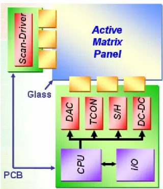
(11) Chapter 1 Introduction. 1.1. LTPS TFTs Nowadays, the amorphous silicon thin film transistors (a-Si TFTs) are commonly used to be the switches of the pixel in active matrix liquid crystal displays (AMLCDs). Fig. 1.1 shows the block diagram of active matrix display. All the driver chips are buried together with the other application-specified ICs on PCB because the current driving capacity of a-Si TFTs is not good enough for the system integration. However, the integration of driver circuitry with display panel on the same substrate is very desirable not only to reduce the module cost but to improve the system reliability. For this reason, the polycrystalline silicon thin-film transistors (poly-Si TFTs) have attracted much attention because of their widely applications in AMLCDs and active matrix organic light-emitting diodes (AMOLEDs) due to its high electron mobility. In poly-silicon film, the carrier mobility larger than 10 cm2/Vs can be easily achieved, which is about tens times larger than that of the conventional amorphous-silicon TFTs (typically below 1 cm2/Vs). This characteristic allows the pixel-switching elements made by smaller TFTs size, resulting in higher aperture ratio and lower parasitic gate line capacitance for the improvement of display performance. Furthermore, the integration of peripheral circuits in display electronics can be achieved by poly-Si TFTs due to its higher current driving capability, which is illustrated in Fig. 1.2. In addition to flat panel displays, poly-Si TFTs have also been applied into some memory devices such as dynamic random access memories (DRAMs), static random 1.
(12) access memories (SRAMs), electrical programming read only memories (EPROM), and electrical erasable programming read only memories (EEPROMs). Among the poly-Si technologies, low temperature polycrystalline silicon thin-film transistors (LTPS TFTs) are primarily applied on glass substrates for the display electrons since higher process temperature may cause the substrate bent and twisted. Fig. 1.3 shows a display panel system. A display panel consists of the following seven function blocks: the multi-source DC-DC converter used to change power input level to different lever supplied for drivers circuitry, the timing controller used to generate control pulses for drivers, the Gamma reference voltages used to generate specific gray-level, the VCOM reference used to supply common voltage, the data drivers for supplying analog voltage to data lines according to input gray-level signals, the scan drivers for switching thin film transistors (TFTs) to select gate lines, the pixel area for displaying image [1]. Low temperature polycrystalline silicon (LTPS) TFTs are higher driving capability and better reliability than amorphous silicon TFTs [2]. Therefore, it is possible to integrate poly-Si TFTs and peripheral driver circuits of display electronics such as active matrix liquid crystal displays (AMLCDs) and active matrix organic light emitting diodes (AMOLEDs) [3]. This is beneficial to fabricate high resolution and high quality displays. However, diverse grain boundary distribution in poly-Si film leads to devices variation. Circuit performance varies with devices variation and will cause non-uniformity of display image. In this thesis, it will be focused on the device variation.. 1.2. Device Variation The LTPS TFTs are found to suffer serious variation of their electrical parameters [4-6]. The poly-Si material is a heterogeneous material made of very small 2.
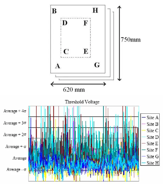
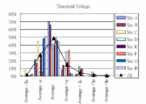
(13) crystals of silicon atoms in contact with each other constituting a solid phase material. These small crystals are called crystallites or grains. The irregular boundaries of these crystallites are the side lines of the grains. Because the material remains solid, the atoms at the border of a crystallite are also linked to the neighbor crystallite ones. However, these atom bonds are disoriented in comparison with a perfect lattice of silicon. This border is called a grain boundary. As the result of various distributions of grain boundaries in the channel of TFTs, the initial characteristics of LTPS TFTs are different from one another, which are shown in Fig. 1.4. The Fig. 1.5 shows site variation of the threshold voltage variation for an LTPS TFT fabrication line plotted in the format of lot trend and the degree of variation can be up to four times of the standard deviation. These variations can be also observed in MOSFETs (Metal-Oxide-Silicon Field Effect Transistors) but they are more critical in LTPS TFTs due to the existence of grain boundary. The device variation will lead to the variation of the circuit performance. It will be reflected directly on the image uniformity of the display. For the circuit design in display, the device variation must be taken into consideration.. 1.3. Motivation The Poly-Si TFTs displays with integrated driving circuits have recently been developed. At present, the poly-Si TFT is the best candidate to realize the system on panel (SOP) and is widely considered for AMLCDs and active matrix organic light-emitting diodes (AMOLEDs). In previous research, it is shown that the LTPS TFTs have some non-ideal characteristics such as device variation. Until to the present time, very few researches have been made on the variation issue of LTPS TFTs. Most researches about LTPS TFTs aim at the improvement of the device performance. However, before LTPS TFTs can be widely-applied in mass production, 3.
(14) yield of the production should be evaluated firstly. The aggressive design strategy will get lower yield while conservative design strategy will underestimate the circuit performance. Consequently, the statistically study of device variation in this thesis is for looking after both yield and circuit performance. It will be reported in the chapter 2 in detail. In conventional circuit simulation with device variation, it is assumed that the device variation is natural and can be represented by Gaussian distribution [7]. But, if the device variation is different from Gaussian distribution [8], how can the circuit simulation with variation put into practice. In the chapter 3, the descriptions of device fluctuation and simulation techniques are proposed. The purpose of these studies is to establish reliable models to estimate precisely on the circuit performance influenced by the device variations. These models will improve the accuracy of the simulation result compared with other simulation models. The simulation techniques will be applied to simulate some benchmark of LTPS TFT circuits such as ring oscillator and differential pair in the chapter 4, and investigate the impact of circuit variation.. 1.4. Thesis Outline Chapter 1.. Introduction. 1.1. LTPS TFTs 1.2. Device Variation 1.3. Motivation 1.4.. Thesis Outline. Chapter 2.. Statistical Descriptions of Device Variation. 2.1.. Introduction to Crosstie TFTs. 2.2.. Statistical Descriptions of Device Variation. 2.3.. The Distribution of Initial Parameter 4.
(15) 2.4.. The Distribution of Initial Parameter Difference. Chapter 3. 3.1.. Simulation Techniques of Device Variation. Simulation Method Review 3.1.1 Worst Case Method 3.1.2 Monte Carlo Method. 3.2.. The Simulation Techniques of Device Variation. 3.3.. Results. Chapter 4.. Effects of Simulation Techniques on TFTs Circuits Performance. 4.1.. Ring Oscillator. 4.2.. Differential Pair. Chapter 5.. Conclusions and Future Works. References. 5.
(16) Fig. 1.1 The block diagram of an active matrix display. Fig. 1.2 The integration of peripheral circuits in a display achieved by poly-Si TFTs. 6.
(17) Data In. Gamma Reference Voltages. Timing Controller. Power In. Multi-Source DC/DC Converter & LDO. Row Drivers. Column Drivers. Display. Fig. 1.3 The display panel system. 7. Vcom Ref.
(18) Fig. 1.4 The initial characteristics of LTPS TFTs are different from one another due to various distributions of grain boundaries. Fig. 1.5 The site variation of the threshold voltage variation for LTPS TFT fabrication line plotted in the format of lot trend 8.
(19) Chapter 2 Statistical Descriptions of Device Variation 2.1. Introduction to crosstie TFTs and Device Fabrication In prior studies, it is known that LTPS TFTs suffered from severe device variation even under well-controlled process. Since the device variation is inevitable in LTPS TFTs, it is essential to classify the sources of variation. In MOSFETs (Metal-Oxide-Silicon Field Effect Transistors), the local variations can be characterized by short correlation distances and global variations characterized by long correlation distances, where the correlation distance is defined as the distance in which a process disturbance affects the device performances. If this distance is lower than the usual distance between devices, the disturbance constitutes a local variation and affects few devices (e.g. a charge trapped in the gate oxide layer). For the global variation, which is characterized by process disturbances with longer correlation distances (e.g. the gate oxide thickness across the wafer surface), affects all the devices within a defined region. Therefore, the devices placed at longer distance are more affected by global variations than devices placed close to each other. In order to investigate the relationship between uniformity issue and device distance, a special layout of the devices adopted in this work is shown in Fig 2.1. The red, blue and yellow regions respectively represent the polysilicon film, the gate metal and the source/drain metal. The structure of the poly-Si film and the gate metal are in the order that resembles the crosstie of the railroad and therefore this layout is called the crosstie type layout of LTPS TFTs. The distance of two nearest active regions is equally-spaced 40µm. The global variation may be ignored within this small distance, and the variation of device behavior can therefore be reduced to only local variation. 9.
(20) For this reason, we can find out the relationship between the variation behaviors and the distance of mutual devices by adopting the crosstie layout TFTs. The process flow of TFTs is described below. Top gate LTPS TFTs with width/length dimension of 20 µm / 5 µm were fabricated using low temperature process. Firstly, the buffer oxide and a-Si:H film with thickness of 50 nm were deposited on glass substrates with PECVD. The samples were then put in the oven for dehydrogenation. The XeCl excimer laser of wavelength 308 nm and energy density of 400 mJ/cm2 was applied. The laser scanned the a-Si:H film with the beam width of 4 mm and 98% overlap to recrystallize the a-Si:H film to poly-Si. After poly-Si active area definition, 100 nm SiO2 was deposited with PECVD as the gate insulator. Next, the metal gate was formed by sputter and then defined. The lightly doped drain (LDD) and the n+ source/drain doping were formed by PH3 implantation with dosage 2 × 1013 cm-2 and 2 × 1015 cm-2 of PH3 respectively. The LDD implantation was self-aligned and the n+ regions were defined with a separate mask. Then, the interlayer of SiNX was deposited. Subsequently, the rapid thermal annealing was conducted to activate the dopants. Meanwhile, the poly-Si film was hydrogenated. Finally, the contact hole formation and metallization were performed to complete the fabrication work. The Fig. 2.2 shows the schematic cross-section structure of the n-type poly-Si TFT with lightly doped drain (LDD).. 2.2. Statistical Descriptions of Device Variation The variability of the observations in a data set is often another important feature of interest when data sets are summarized. We now consider several summary measures of variability, sometimes also called measures of dispersion or spread.. 2.2.1. Variance and Standard deviation 10.
(21) The most commonly used measure of variability in statistical analysis is called the variance. It is a measure that takes into account all the observations in a data set. The variance s2 is expressed in units that are the square of the units of measure of the variable under study. Take the positive square root of the variance, and the resulting value is called the standard deviation and is also used as a measure of variability.. 2.2.2. Range The range is the difference between the largest and smallest observations in a data set. A limitation of the range as a measure of the variability of a data set is that it depends only on the largest and smallest observations quite close to each other with the exception of one outlying observation. Despite the concentration of almost all the observations, the range would be large because of the one outlying observation. Another limitation of the range as a measure of variability is that it is affected by the number of observations in the data set. The larger the number of observations, the larger the range tends to be. Sometimes, the range of a data set is indicated by presenting the smallest and largest observations in the data set. This form of presentation not only provides information about the variability of a data set but also provides information about the location of the data set distribution.. 2.2.3. Inter-quartile Range Because the range depends only on the smallest and largest observations in a data set, a modified range is sometimes used that reflects the variability of the middle 50 percent of the observations in the array. This modified range is called the inter-quartile range. The inter-quartile range is the difference between the third and first quartiles of the data set. The inter-quartile range may be considered to be approximately the range for a trimmed data set in which the smallest 25 percent and 11.
(22) the largest 25 percent of observations have been removed.. 2.3. The Distribution of Initial Parameter Firstly, we introduce the statistical expressions for the following analysis. The average value µ is defined as n. ∑x. X = i=1 n. Where x is the observe value. (2-1). The standard deviation value, σ, is usually used to investigate the distribution of the observed value. The standard deviation value is given as. σ≡. 2 1 x− X) ( ∑ n n. Where x is the observe value. (2-2). In order to obtain the more accurate parameter distributions of crosstie layout TFTs, large amount of device parameters are required. In this work, more than six hundred of devices were measured within 45µm on the glass substrate. The distributions of VTH and Mu of measured devices are shown respectively in Fig. 2.3 (a), (b), and Fig. 2.4 (a), (b). The average and standard deviation of VTH of n-type are 1.69 V and 0.03 V, and those of p-type are -2.41 V and 0.05 V. On the other hand, the average and standard deviation of Mu of n-type are 59.66 cm2 /Vs and 7.84 cm2/Vs, and those of p-type are 75.31 cm2 /Vs and 2.29 cm2/Vs, accordingly. These figures reveal that the distributions of VTH and Mu are asymmetric and non-Gaussian, and there is no fit equation to represent the variation. In particular, the distributions of Mu have higher degree of skew than VTH. Compared p-type with n-type devices, the distributions of VTH and Mu are both less asymmetric in the p-type than in the n-type devices. Especially, the distribution of VTH of the p-type devices approximates to Gaussian distribution. However, it is so difficult to model the variable behavior that the circuit simulation can not be put into practice. 12.
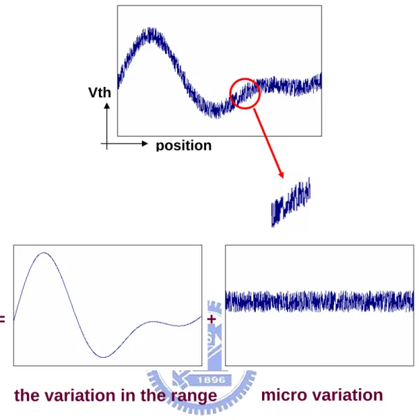
(23) Let me take a look in Fig. 2.5, it indicates that the distributions of initial parameters vary with the different sites on glass and lot. If we want to find the variation behaviors with respect to the distance, it can not just classify them via these distributions. Another grouping method mentioned in the next section will get the more identical distributions, which will be more useful to evaluate the variations in LTPS TFTs.. 2.4. The Distribution of Initial Parameter Difference Return to analyze initial VTH and Mu of the measured devices with position, those are shown respectively in Fig. 2.6 (a) and (b). Fig. 2.6 (a) and (b) reveal VTH and Mu of the measured devices vary irregularly with position, and the variable behaviors are like signal and noise. The noise such as the micro variation is the distributions of the difference of device parameters. The concept of the description of device parameter variation will be proposed as shown as Fig. 2.7. The signal such as the variation in range is determined by gate insulator thickness, ion implantation dosage, channel length, LDD length and so on. The noise such as the micro variation is determined by defect sites, defect density, activation efficiency and so on. If it can find that fit equations used to describe the distributions of the difference of device parameters, the noise in circuit simulation will randomly generate from them. Therefore the distributions of the difference of VTH and Mu for device pairs of the measured devices are described below. In order to identify the effects of the global and local variation, the parameters differences of two devices under certain distance are divided with several groups according to the distance between two devices. In prior studies, the averages of parameters differences stand for global variation of LTPS TFTs, while the standard 13.
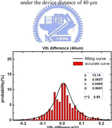
(24) deviation of parameter differences shows the local variation in the devices. In this thesis, we characterize the global variation and local variation as the variation in the range and micro variation for the analysis of LTPS TFTs, respectively. Fig. 2.8 and Fig. 2.9 show the average and the standard deviation of the differences of VTH and Mu. As the mutual device distance increases, the deviations of device differences are not changing with the device distance. It can be explained that the micro variation will merely vary with distance as we expect. As for the variation in a range, these figures show the diverse results. In the difference of VTH, the average is increasing with device distance. However, the average of the difference of Mu seems no significant trend when the distance of mutual devices is increasing. Although the averages of the differences of these parameters show different behaviors, they still appear in linear form. On the other hand, the effects of variation in a range are still minor than those of the micro variation under short device distance. Since these conditions differ from device to device, the micro variation will lead to the random distribution of device parameters. For the circuit simulation, Monte Carlo method is generally adopted. However, the worst case simulation will be more suitable when the variation in a range of device is increasing. In Fig. 2.10 and Fig. 2.11, the distributions of the difference of (a) VTH and (b) Mu can be used to describe the micro variation of the measured devices. According to these figures, the shape of these distributions is symmetrical and looks like Gaussian distribution. The range of these distributions is wider than triple standard deviation of Gaussian distribution so these distributions are not Gaussian distribution. Furthermore, there are some uncommon equations similar with Gaussian distribution, and they are more suitable to describe the variation behavior. In next work, the square of the correlation coefficient (R square) presenting the fitness from the chosen 14.
(25) equation will be used. R square is defined as. r2 =. SSR SSE = 1− , where SST SST. (2-3). SSR = ∑ ( ˆy − y )2 = ∑ Yˆ 2 = b12 ∑ X 12 + b22 ∑ X 22 + 2b1b2 ∑ X 1 X 2 SST = ∑ ( y − y )2 SSE = ∑ eˆ 2 = ∑ ( yi − ˆyi )2. R square which indicates the similarity between the proposed model and the real data, and its value ranges between 0 and 1 [9]. It represents the proposed model is more similar with real data when R square value much approaches to 1. Generally speaking, the values of R square above 0.7 represnent the good fitness for the chosen funcion. Two models are proposed to fit these two distributions, and the square of the correlation coefficient (R square) can reach near 0.9. Consequently, the difference of VTH follows the distribution of Gaussian-Lorentzian cross product, which is y=. a 2 ⎛ ⎞ ⎛ ⎞ − − x b 1 x b ⎛ ⎞ ⎛ ⎞ ⎟ ⎜1 + d ⎜ ⎟ ⋅ exp⎜ (1 − d ) ⋅ ⎜ ⎟ ⎟ ⎜ ⎟ ⎜ ⎟ c 2 c ⎝ ⎠ ⎝ ⎠ ⎝ ⎠ ⎝ ⎠ 2. (2-4). Where a is the peak value of the distribution b is the center of the distribution c is fitting parameter related to the width of the distribution d is fitting parameter varying from 0 to 1; 0 represent the pure Gaussain function while 1 is a pure Lorentzian distribution On the other hand, the difference of Mu follows Lorentzian distribution, which is. 15.
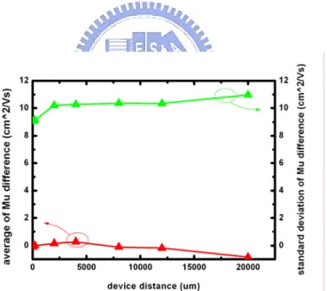
(26) y=. a ⎛x −b⎞ 1+ ⎜ ⎟ ⎝ c ⎠. (2-5). 2. Where. a is the peak value of the distribution b is the center of the distribution c is fitting parameter related to the width of the distribution Where the parameters a, b, c, and d are fitting parameters and vary slightly with distance. These two distributions are more concentrated than the commonly known Gaussian distribution, and the peaks of these are sharper. We polt the fitting results with different device distance in Fig. 2.12 (a) ~ (d) and Fig. 2.13 (a) ~ (d) for the distributions of the differences of Vth and Mu, respectively. The values of R squre of the above fittng curves both reach near 0.9. It clearly shows the good fitness of our proposed mathemtical model. Most of the fitting parameters slightly changing with distance supports the effects of the variation in the range are minor than those of micro variation we mentioned before. However, we still have to notice that micro variation increasing rapidly with distance and saturate about the device distance of 2000 µm. This finding will affect the result of the circuit simulation. For above reasons, how to apply the proposed model in circuit simulation is very critical and important. There are several methods of parameter generation in next section.. 16.
(27) Fig. 2.1 The layout of the crosstie TFTs. Fig. 2.2 The schematic cross-section structure of the n-type poly-Si TFT with lightly doped drain. 17.
(28) Fig. 2.3 (a) The distributions of threshold voltage of n-type devices for crosstie TFTs. Fig. 2.3 (b) The distributions of threshold voltage of p-type devices for crosstie TFTs. 18.
(29) Fig. 2.4 (a) The distributions of mobility of n-type for crosstie TFTs. Fig. 2.4 (b) The distributions of mobility of p-type for crosstie TFTs. 19.
(30) Fig. 2.5 The distributions of initial parameters vary with the different sites on glass and lot. 20.
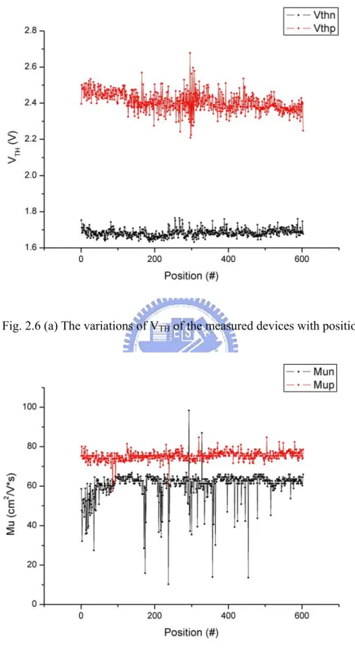
(31) Fig. 2.6 (a) The variations of VTH of the measured devices with position. Fig. 2.6 (b) The variations of mobility of the measured devices with position. 21.
(32) Vth. position. =. +. the variation in the range. micro variation. Fig. 2.7 The concept of the proposed description of device parameter. 22.
(33) Fig. 2.8 The average and the standard deviation of the differences of threshold voltage. Fig. 2.9 The average and the standard deviation of the differences of mobility. 23.
(34) Fig. 2.10 (a) The distribution of VTH difference of n-type devices and its fitting curve under the device distance of 40 µm. Fig. 2.10 (b) The distribution of VTH difference of p-type devices and its fitting curve under the device distance of 40 µm. 24.
(35) Fig. 2.11 (a) The distribution of Mu difference of n-type devices and its fitting curve under the device distance of 40 µm. Fig. 2.11 (b) The distribution of Mu difference of p-type devices and its fitting curve under the device distance of 40 µm. 25.
(36) Fig. 2.12 (a) The distribution of VTH difference of n-type devices and its fitting curve under the device distance of 200 µm. Fig. 2.12 (b) The distribution of VTH difference of n-type devices and its fitting curve under the device distance of 2000 µm. 26.
(37) Fig. 2.12 (c) The distribution of VTH difference of p-type devices and its fitting curve under the device distance of 200 µm. Fig. 2.12 (d) The distribution of VTH difference of n-type devices and its fitting curve under the device distance of 2000 µm. 27.
(38) Fig. 2.13 (a) The distribution of Mu difference of n-type devices and its fitting curve under the device distance of 200 µm. Fig. 2.13 (b) The distribution of Mu difference of n-type devices and its fitting curve under the device distance of 2000 µm. 28.
(39) Fig. 2.13 (c) The distribution of Mu difference of p-type devices and its fitting curve under the device distance of 200 µm. Fig. 2.13 (d) The distribution of Mu difference of p-type devices and its fitting curve under the device distance of 2000 µm. 29.
(40) Chapter 3 Simulation Techniques of Device Variation. 3.1. Simulation Methods Review There are two major methods of simulation to analyze circuit performance, which are the worst-case and Monte Carlo analysis as described below [11].. 3.1.1. Worst-Case Method Worst-Case analysis is the most commonly used technique in industry for considering manufacturing process tolerances in the design of integrated circuits. These approaches are relatively inexpensive compared to the yield maximization approaches in terms of computational cost and designer effort, and they also provide high parametric yields. At any design point, uncontrollable fluctuations in the circuit parameters cause circuit performance to device from their nominal design values. The goal of worst case analysis is to determine the worst values that the performance may have under these statistical fluctuation. In addition to finding the worst-case values of the circuit performance, this analysis also finds the corresponding worst-case values of noise parameters. A noise parameter is treated as a random variable. Any random variable is characterized by probability density function (and by a mean and a standard deviation which depends on the density function), as shown in Fig. 3.1. The worst-case noise parameter vector is used in circuit simulation to verify whether circuit performances are acceptable under these conditions. Similar to worst-case analysis, one can also perform best-case analysis. In fact, industrial designs are often simulated under best, worst, and nominal noise parameter conditions, which provide designers with quick estimates of range of variation of circuit performances. 30.
(41) 3.1.2. Monte Carlo Method Yield, expressed as a multi-dimensional integral, can be evaluated numerically using either the quadrature-based, or Monte Carlo based methods. The quadrature-based methods have computational costs that explode exponentially with the dimensionality of the statistical space. Monte Carlo methods, on the other hand, are less sensitive to the dimensionality. The Monte Carlo method is a computer simulation of real distributions of random noise parameters, and it is the simplest, most reliable and accurate of all methods used in practice, but for high accuracy it requires a large number of sample points. Typically, hundreds of trials are required to obtain reasonable accurate yield estimation. For nonlinear and/or time domain circuit analysis, this is computational expensive. Hence, a fundamental problem to solve is to increase the efficiency of the Monte Carlo method and its accuracy, measured by the variance of the yield estimation.. 3.2. The Simulation Techniques of Device Variation There are two major methods of simulation to analyze circuit performance, which are the worst-case and Monte Carlo analysis as described below. The notations of the parameters generations are shown in Fig. 3.2. There are four kind descriptions of the parameters generations. First, it is picking up the parameters randomly from the measured database, and calls “Look up table.” Look up table (LUT) is most direct method, but it is complicated and costs much time. The concept of look up table parameters generation is shown in Fig. 3.3. But a ring oscillator is a special case, and it needs to choose one series of initial parameter in order as 1st class and randomly choose another series of initial parameter in order as 2nd class. 31.
(42) Second, the Monte Carlo simulation of Gaussian distribution is a conventional method [10]. It needs to calculate mean and standard deviation of the measured data, and picks up the parameters randomly from Gaussian distribution based on mean and with triple standard deviation range. In general, Gaussian distribution is commonly used for circuit simulation. However, the behavior of the variation is different from Gaussian distribution, and the conventional method might not suitable enough to simulate for the circuits performance with device variation. Third, modified Gaussian distribution which is adjusted by inter-quartile range might be used. Because the distributions are more concentrated than the commonly known Gaussian distribution, triple standard deviation range may be not precise enough to define the percentage of all parameters. Therefore, inter-quartile range [9], a fixed range, always is a definition of fifty percent of all parameters and used to modify conventional Gaussian method. The modified Gaussian sigma is defined as Modified Gaussian Sigma = (Inter − quartile range * 68 / 50) / 2. (3-1). The parameters simulation conditions of Gaussian and modified Gaussian are list in Table 3.1 and Table 3.2, respectively.. NTFT. PTFT. Value. Value. VTH (V). 1.69±0.09. -2.41±0.16. Mobility (cm2/Vs). 59.66±23.52. 75.31±6.87. Parameters (Gaussian). Table 3.1 Means and standard deviations of Gaussian. 32.
(43) NTFT. PTFT. Value. Value. 1.69±0.04. -2.41±0.15. (0.09). (0.16). 59.66±6.75. 75.31±5.78. (23.52). (6.87). Parameters. VTH (V). Mobility (cm2/Vs) Table 3.2 Means and standard deviations of modified Gaussian Compare modified Gaussian with Gaussian, there are the same mean values of modified Gaussian and Gaussian, but triple standard deviation value of modified Gaussian and Gaussian are very different. Especially, both threshold voltage and mobility of NTFT are larger different between Gaussian and modified Gaussian than those of PTFT. Although modified Gaussian has concentrated the distribution, it cannot include the extreme value of the parameters. Finally, signal-noise is a new description of device parameter variation in circuit simulation will be proposed. Due to above section, the variation behavior is like signal and noise. The concept of signal-noise parameter generation is shown in Fig. 3.4. Take anyone initial value as signal, and add parameters picked up randomly from the equations, which above section have mentioned that used to describing the difference of the distributions of the measured data. The overall flow of parameters generations are shown in Fig. 3.5. Especially, one ring oscillator randomly chose one initial parameter as signal, and another ring oscillator randomly chose another one as signal. According to the statistical relationship, which represent in equation 3-2, the standard deviation of noise in a series is divided into even and odd two groups, it reveals that noise generated from the proposed distribution of parameter difference has to divide by √2. 33.
(44) σe =. σo =. ∑ ( x − X). 2. n. n. ∑ ( x − X). 2. n. n. σ o −e 2 = σ o 2 + σ e 2 − 2σ oe Qσ oe = 0, σ o = σ e. σ = 2σ o 2 = 2σ e 2 = 2σ 2. σ=. σ o −e. (3-2). 2. 3.3. Results Then, the fitness of above descriptions of device parameters generations can use Kolmogorov-Smirnov Tests. Kolmogorov-Smirnov Tests are commonly used to test for verifying that a sample comes from a population with some known distribution and also that two populations have the same distribution. In Kolmogorov-Smirnov Test, it defines maximum vertical distance between the empirical and true cumulative distribution function of the proposed, and p-value such as the probability of the similarity is transformed from the cumulative distribution function. P-value which indicates the fitness between the proposed distribution and the measured data, and its value ranges between 0 and 1. It represents the proposed distribution is more similar with measured data than others when p-value much approaches to 1, but p-value is not proportional to the fitness [12]. Generally speaking, if p-value is smaller than 0.05, it will represent that this sample does not come from the measured data. In other words, the empirical distribution function is too far from the true cumulative distribution function of the real distribution, and two 34.
(45) distributions are very different. The p-values such as the fitness of the parameters including VTH, Mu, and the difference of VTH and Mu are shown in Fig. 3.6 and classified according to the description of the parameters generations. It reveals that the distribution of parameters generated from look up table is the most similar with the measured data. The next most similar is the distribution of parameters generated from signal-noise. Gaussian as conventional method is the least suitable for generating parameters in circuit simulation with variation, but VTH of the p-type device is a little similar with Gaussian distribution and its p-value is bigger than 0.05. The fitness of modified Gaussian lies in between the p-value of signal-noise and Gaussian, but it only refers to the p-value of some parameters like the difference of VTH and Mu, except Mu of n-type from modified Gaussian. In some circuits of the display panel layout, the devices of circuit are close to each other; as a result, the descriptions of devices variation in above section will put into practice.. 35.
(46) Fig. 3.1 Probability density function for (a) a Gaussian and (b) a uniform random variable. 36.
(47) Look Up Table (LUT). Gaussian. Modified Gaussian. Signal-Noise. Randomly pick up the parameters from the measured data.. Randomly pick up the parameters from Gaussian distribution based on mean and standard deviation of the measured data.. Randomly pick up the parameters from modified Gaussian distribution based on mean and inter-quartile range of the measured data.. Take initial value as mean and add parameters picked up randomly from the equations describing the difference of the measured data.. Put into the spice simulation for circuit performance prediction.. Fig. 3.2 The notations of the parameters generations. 37.
(48) Fig. 3.3 The concept of look up table parameters generation. Fig. 3.4 The concept of signal-noise parameters generation. 38.
(49) Fig. 3.5 The flow of parameters generations. 39.
(50) Fig. 3.6 The fitness of four descriptions of parameters generations. 40.
(51) Chapter 4 Effects of Simulation Techniques on TFTs Circuits Performance. In this section, take some benchmark of LTPS TFT circuits for example and investigate the impact of circuit variation with different descriptions of device parameters generations. This section is divided into two parts. In Part I, a digital circuit such as ring oscillator is simulated and discussed circuit performance with variations. In Part II, an analog circuit such as differential pair is simulated and discussed circuit performance with variations.. 4.1. Ring Oscillator Ring Oscillator will be taken for example in this part because it is a basic digital circuit and widely used in driving circuit in display. Ring Oscillator, as shown as Fig. 4.1, is always formed by connection an odd number of inverters in a loop to make the oscillation [13]. If it is composed of more devices, the oscillating period will be longer. In order to easily measure, a ring oscillator will be improved by (a) NAND and (b) buffer circuit as shown as Fig. 4.2 (a) and (b). So the circuit performance like the oscillating period of ring oscillator is an average effect of all devices, they are less sensitive to the difference of device parameters. To compare the effects of the device variation on circuit performance, four descriptions of parameters generations proposed in previous section are adopted in circuit simulation here. It concerns about the average time delay in each gate of a ring. 41.
(52) oscillator, and that can be given by. Delay in each stage : t d =. oscillating period 2 ⋅ number of devices. (4-1). In this example, a ring oscillator is composed of 105 CMOS inverters, and simulated with four descriptions of parameter distributions. Besides, each description of parameter distributions is simulated by Monte Carlo method for 30 times with 5 V and 15 V. It is because that concerns about not only the statistical profile of each description of parameter distributions, but also how does a ring oscillator work on two different operating points. Because of the sharper distribution of the difference of VTH and Mu in reality than Gaussian, mean and standard deviation of delay in each stage might be not complete enough to represent the circuit performance. For that reason, the box plot which exhibits much information may be used here, and it also can roughly describe the distribution profile of time delay in each stage. The box plot generally shows mean, median, 25th and 75th percentiles, and extreme value in a single chart. Mean is shown as a square in the box, but median is shown as a line across the box. The box stretches from the lower outline which is defined as the 25th percentile to the upper outline which is define as the 75th percentile. The bar below the box is defined as the 5th percentile, and the opposite bar over the box is defined as the 95th percentile. Moreover, the extreme values such as minimum and maximum are signed as stars. Consequently, the box plot is the best profile to represent the nature of the data and parallel box plots are very useful for comparing distributions. The simulation results of ring oscillator with (a) 5V and (b) 15V using four kind descriptions of parameter generations are shown respectively in Fig. 4.3 (a) and (b). Compared Fig. 4.3 (a) with Fig. 4.3 (b), average delay times in each stage, which are the simulation results of ring oscillator, vary with different power supply VDD. 42.
(53) Nevertheless, for the four descriptions, the profiles resulted from a same description of parameter distribution with different VDD resemble each other. In Fig. 4.3 (a) and Fig. 4.3 (b), there are the gaps between the average delay times due to different simulation techniques with the same VDD. Because the gaps can be eliminated by adjusting VDD, the simulation results may be more interested in its profile. The profiles of delay time resulted from simulated with the conventional Gaussian and modified Gaussian are both more concentrative than LUT, especially modified Gaussian, because those two simulation techniques can not consider the variation in range. On the contrary, because of considering the variation in range, the profile of the simulation result from signal-noise is most similar with that from LUT. In Fig. 4.4, signal-noise, signal-small, and signal-big respectively refer that signals are randomly generated form initial parameter database, only micro variation, and large variation in the range. It is said that signal-noise simulation technique might be useful to represent the real data, and the circuit performance of a ring oscillator might be dominated by the device variation in range.. 4.2. Differential Pair In the integrated circuit application, coupling effect is a serious problem for signal transmission [13]. Fig. 4.5 (a) shows that clock will couple some noise to adjacent signal line during the rising and falling time. If we transmit the difference of signal by two separated signal lines shown in Fig. 4.5 (b), the coupling effect of clock will be cancelled by getting the difference of the signal. For this reason, the differential pairs are widely used for analog circuit design because of the immunity for the noise. For the display applications, the differential pairs are commonly used in every block of display electronics such as the input stage of OP amplifier, driving 43.
(54) circuit and so on. Fig. 4.6 shows the basic differential pair structure, where RD is resistive load and Rss represents the output impedance of current bias; differential signals are applied to the gate terminal of transistor M1 and M2. The differential pairs ideally use two matched devices to eliminate the effect of the noise in common mode, so they are sensitive to the difference of device parameters. To compare the effects of the device variation on circuit performance, four descriptions of parameters generation proposed in previous section are adopted in circuit simulation here. It concerns about the common mode reject ratio (CMRR) of a differential pair, and that can be given by: A dm ≅ CMRR = A cm−dm. W (VGS − Vth ) 2 Rss L µ∆Vth + ∆µ (VGS − Vth ). µ (VGS − Vth ) + 2 µ 2 C ox. (4-2). The simulation results of CMRR with these four methods are shown in Fig. 4.7. It is attributed to the sharper distribution of the difference of VTH and Mu in reality than Gaussian. Therefore, it was found that the curves of the cumulative probability resulted from LUT and Gaussian exhibit a difference of 10 dB in average and cross at about 55 dB. All the curves of the cumulative probability resulted from LUT, modified Gaussian, and signal-noise are very similar, except the range from 50 dB to 70 dB. But there is a little difference between the curves of the cumulative probability from LUT and signal-noise. In other words, they are most similar than others. In commercial using, the circuit performance of the differential pairs usually focuses on the yield of CMRR below 60dB. According to these simulation results from LUT, Gaussian, modified Gaussian, and signal-noise, the yields of CMRR below 60 dB are 86%, 73%, 99% and 91% respectively. As for the average performance, simulation adopting Gaussian distribution might give an underestimated prediction. On the contrary, that adopting modified Gaussian might give an overestimated prediction. The circuit performance of simulation with signal-noise 44.
(55) variation approaches close to that with LUT even though it might be a little overestimated prediction below 70 dB. It is said that signal-noise simulation technique might be useful to represent the real data, and the circuit performance of differential pair might be dominated by micro variation of devices. The parameter generation of signal-noise in circuit simulation can also be used to evaluate the performance of other driving circuit of AMLCD and AMOLED by using matched TFTs [14].. 45.
(56) 1. 0. 1. 0. 1. Fig. 4.1 The simple ring oscillator circuit. Logic 1 ~ inverter Fig. 4.2 (a) A ring oscillator improved by NAND circuit. R=1000K C=2p Fig. 4.2 (b) The buffer circuit of a ring oscillator. 46. 0 <> 1.
(57) Fig. 4.3 (a) Circuit performance of ring oscillator simulated from four descriptions of simulation techniques. (VDD = 5 V). 47.
(58) Fig. 4.3 (b) Circuit performance of ring oscillator simulated from four descriptions of simulation techniques. (VDD = 15 V). 48.
(59) Fig. 4.4 Compared signals of different variability in the range. 49.
(60) Fig. 4.5 (a) The coupling effects of the clock signal. Fig. 4.5 (b) The signal transmission is done by differential signal. 50.
(61) Fig. 4.6 Basic differential pair structure. 51.
(62) Fig. 4.7 The simulation results of CMRR with four descriptions of parameters generations. 52.
(63) Chapter 5 Conclusions and Future Works. A new model, which is using the signal-noise concept, has been proposed to describe device variation of the LTPS TFTs by the differences in VTH and Mu of the LTPS TFTs. Then the new model has been applied to a new proposed description of parameter generation in circuit simulation. Compare four kind descriptions of parameters generations, it reveals that the distribution of parameters generated from look up table and signal-noise are similar with the measured data. Gaussian as conventional method is the least suitable for generating parameters in circuit simulation with variation. As four kind descriptions of parameters generations are adopted in circuit simulation, it reveals that the circuit performance of a digital circuit, such as ring oscillator, is dominated by the variation in range. On the other hand, the circuit performance of an analog circuit, such as differential pair, is dominated by micro variation of devices. According to all circuit simulation results, signal-noise simulation technique is useful to represent the real data. The parameter generation of signal-noise in circuit simulation can also be used to evaluate the performance of other driving circuit of AMLCD and AMOLED by using matched TFTs. In the future, we can investigate the description of macro variation and the detailed causes of macro and micro variation. We can also measure practical circuit and find statistic method to predict yield and circuit performance relationship.. 53.
(64) References [1] L. W. MacDonald and A. C. Lowe, “Display System: Design and Applications”, Wiley, 1997. [2] Y. Nakajima, “Latest Development of “System-on-Glass” Display with Low Temperature Poly-Si TFT,” SID Tech. Dig., pp. 864, 2004. [3] H. Oshima and S. Morozumi, “Future trends for TFT integrated circuit on glass substrate,” IEDM Tech. Dig., pp. 157, 1989. [4] Kitahara, Yoshiyuki, Toriyama, Shuichi, Sano, Nobuyuki, “A new grain boundary model for drift-diffusion device simulations in polycrystalline silicon thin-film transistors”, Japanese Journal of Applied Physics, Part 2: Letters, v 42, n 6 B, pp. L634-L636 (2003). [5] Wang, Albert W. and Saraswat, Krishna C., “Modeling of grain size variation effects in polycrystalline thin film transistors”, Technical Digest – International Electron Devices Meeting, pp. 277-280 (1998). [6] Wang, Albert W. and Saraswat, Krishna C., “Strategy for modeling of variations due to grain size in polycrystalline thin-film transistors”, IEEE Transactions on Electron Devices, v 47, n 5, pp. 1035-1043 (2000). [7] Kenichi Okada, Kento Yamaoka, and Hidetoshi Onodera, “Statistical modeling of gate-delay variation with consideration of intra-gate variability”, Proceedings IEEE International Symposium on Circuits and Systems, v 5, pp. V513-V516, 2003. [8] Shi-Zhe Huang, “Statistical Study on the Uniformity Issue of Low Temperature Polycrystalline Silicon Thin Film Transistor”, Diss. National Chiao Tung University, pp. 14, 2005. [9] Devore, “Applied Statistics for Engineers and Scientists”, Thomson, Second Edition, 2005. [10] Saeed Ghahramani, “Fundamentals of Probability”, Prentice-Hall, Second Edition, 2000. [11] J. C. Zhang, M. A. Styblinski, “Yield and variability optimization of integrated circuits,” Kluwer Academic Publishers, 1995 [12] D. C. Montgomery, G. C. Runger, N. F. Hubele, “Engineering Statistics”, John Wiley, Third Edition, 2004. [13] Adel S. Sedra and Kenneth C. Smith, “Microelectronic Circuits”, Oxford, Fourth Edition, 1998. 54.
(65) [14] Woo-Jin Nam, Sang-Hoon Jung, Jae-Hoon Lee, Hye-Jin Lee, and Min-Koo Han, “A Low-Voltage P-type Poly-Si Integrated Driving Circuits for Active Matrix Display”, SID Tech. Dig., pp. 1046-4049 (2005).. 55.
(66) 學 經 歷. 姓 名:陳 琬 萍 性 別:女 生 日:民國七十一年四月二十二日 地 址:台南市永華二街41巷14號. 學 歷:國立交通大學運輸科技與管理學系(89.9~93.6) 國立交通大學顯示科技研究所碩士班(93.9~95.6). 碩士班論文題目:對應低溫多晶矽薄膜電晶體變動性之 電路模擬技術之研究 (Study on the Circuit Simulation Techniques Corresponding to the Variation of LTPS TFTs). 56.
(67)
數據

+7
相關文件
了⼀一個方案,用以尋找滿足 Calabi 方程的空 間,這些空間現在通稱為 Calabi-Yau 空間。.
You are given the wavelength and total energy of a light pulse and asked to find the number of photons it
Reading Task 6: Genre Structure and Language Features. • Now let’s look at how language features (e.g. sentence patterns) are connected to the structure
好了既然 Z[x] 中的 ideal 不一定是 principle ideal 那麼我們就不能學 Proposition 7.2.11 的方法得到 Z[x] 中的 irreducible element 就是 prime element 了..
Wang, Solving pseudomonotone variational inequalities and pseudocon- vex optimization problems using the projection neural network, IEEE Transactions on Neural Networks 17
volume suppressed mass: (TeV) 2 /M P ∼ 10 −4 eV → mm range can be experimentally tested for any number of extra dimensions - Light U(1) gauge bosons: no derivative couplings. =>
Define instead the imaginary.. potential, magnetic field, lattice…) Dirac-BdG Hamiltonian:. with small, and matrix
• Formation of massive primordial stars as origin of objects in the early universe. • Supernova explosions might be visible to the most
