半導體非對稱雙量子井結構中之自旋相依能階分裂
53
0
0
全文
(2) 半導體非對稱雙量子井結構中之自旋相依 能階分裂 Spin Orbit Splitting of Energy Levels in Semiconductor Asymmetric Double Well Structure 研究生: 陳啟暉. Student : Chi-Huei Chen. 指導教授:霍斯科 博士 Advisor : Dr. Oleksandr Voskoboynikov. 國立交通大學 電子工程學系 電子研究所碩士班 碩士論文 A Thesis Submitted to Department of Electronics Engineering College of Electrical Engineering and Computer Science National Chiao Tung University In Partial Fulfillment of the Requireements For the degree of Master of Philosophy In Electronics Engineering June 2005 Hsinchu, Taiwan, Republic of China. 中華民國九十四年六月.
(3) 致謝 碩士班兩年的研究生活一眨眼間就結束了,這兩年的生活裡有甘也 有苦,過地十分踏實,而其中最高興的莫過於能遇到霍斯科教授,他 博學的知識以及對物理的熱愛都在我研究生的生涯裡深深地影響著 我。 在實驗室裡,我必須感謝李秉奇學長和林志昌學長,經由和你們的 討論,讓我增長了許多關於半導體和物理方面的知識。還有其他關心 我的學弟妹和朋友們,謝謝你們平日的幫忙。 此外,我還要特別感謝我的學弟清揚和弘毅,謝謝你們在最後這幾 個月裡的全力支持,少了你們的支援這篇論文絕對無法如期誕生。 最後,當然要感謝我的父母,由於你們的支持,我才得以全心地投 入我的課業,並在最後順利地完成學業。.
(4) Acknowledgement To meet Professor Voskoboynikov is the best event in National Chiao Tung University in the past two years. In the first discussion with Professor Voskoboynikov, I still could not make the decision to join his research team because his research topics were totally strange for me at that time. And I asked him if I can discuss with him if I have problems finally. “Sure! You can ask me anything you don’t understand.”, he replied. This is why I join his research team. I still do not know how to express my appreciation for everything done by Professor Voskoboynikov until now. But I have to say that not only the master’s degree but the research life in the past two years will not exist without you definitely. Thank you, Professor!.
(5) 半導體非對稱雙量子井結構中之自旋相依能階分裂 學生 : 陳啟暉. 指導教授 : 霍斯科博士 國立交通大學 電子工程學系 電子研究所碩士班. 摘要. 在本篇論文中的絕大部分將致力於分析以往不曾被探討過的半導體非對稱雙 量子井結構中之自旋相依能階分裂。跟隨著 E. A. de Andrada e Silva 先前於 半導體非對稱量子井結構中之自旋相依電子狀態分裂的工作成果,我們試圖去呈 現半導體非對稱雙量子井結構中之自旋相依能階分裂並示範如何去調整自旋相 依能階分裂的大小以實現實際的自旋電子學元件。 源自於八個能帶的 Kane 模型之標準封包函數讓我們得以研討在 III-V 族半導 體非對稱雙量子井結構中電子色散關係之自旋相依能階分裂。我們從亦為導電帶 和價電帶中的兩種成分之封包函數的似薛丁格方程式之有效質量 Hamiltonian 運算子開始我們的研究。最後憑藉著分別對於自旋向上以及自旋向下的數值解, 我們呈現出在 Al x In 1- x Sb/InSb/Al y In 1- y Sb/InSb/Al y In 1- y Sb 的結構中自旋相依能階 分裂的值會如何隨著不同的參數值做變化。.
(6) Spin Orbit Splitting of Energy Levels in Semiconductor Asymmetric Double Well Structure Student: Chi-Huei Chen. Advisor: Dr. Oleksandr Voskoboynikov. Department of Electronics Engineering and Institute of Electronics National Chiao Tung University Abstract In this paper we devote the most of it to the analysis of spin-orbit interaction in low dimensional semiconductor asymmetric double well structure which has never been done before. Following the previous work of spin-orbit splitting of electronic states in semiconductor asymmetric quantum wells by E. A. de Andrada e Silva, we attempt to present the spin-orbit splitting of electronic states in the semiconductor asymmetrical double well and demonstrate how to adjust the amplitude of the spin-orbit splitting in order to have a real spintronics device. The spin-orbit splitting in the dispersion relation for electrons in III-V semiconductor asymmetric double well is studied within the standard envelope function formalism starting from the eight-band Kane model for the bulk. We start our investigation from the effective mass Hamiltonian which is the Schrödinger-like equation for the two components of the conduction band envelope function. At last we show how the spin-orbit splitting will vary with different parameters in Al x In 1- x Sb/InSb/Al y In 1- y Sb/InSb/Al y In 1- y Sb asymmetric quantum wells by solving the solutions for both spin up and spin down numerically..
(7) Contents Chapter 1. Introduction and Motivations-------------------------------1. Chapter 2. Theory-------------------------------------------------------------------9. 2.1 The k • p method---------------------------------------------------------------------------9 2.2 Kane’s model for band structure-----------------------------------------------------12 2.3 The Spin Orbit Interaction-------------------------------------------------------------18. Chapter 3. Results ----------------------------------------------------------------24. 3.1 Asymmetrical Square Double Well--------------------------------------------------24 3.2 The Energy Levels and Spin Splitting in the Asymmetric Double Well Structure------------------------------------------------------------------------------------28 3.3 The Variation of the Barrier Width in the Asymmetric Double Well----------32 3.4 The Variation of the Barrier Height in the Asymmetric Double Well---------37. Chapter 4 References. Conclusion----------------------------------------------------------41.
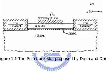
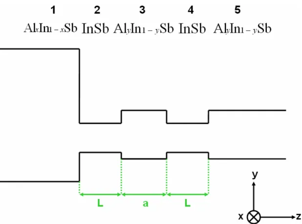
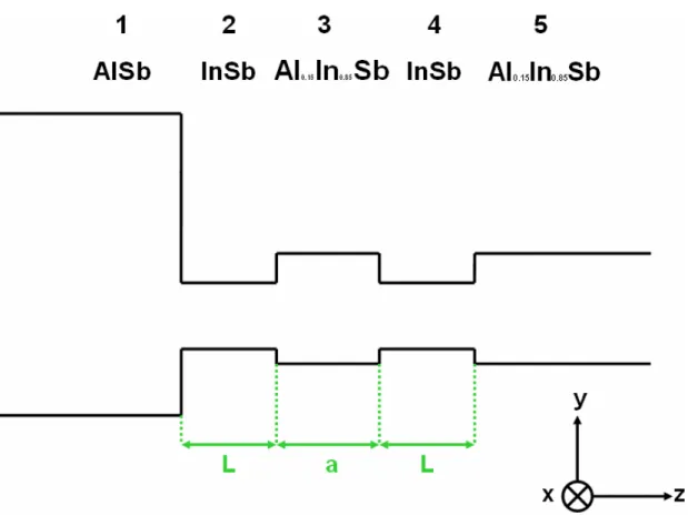
(8) Figure 1.1 The Spin transistor proposed by Datta and Das Figure 1.2. The InSb quantum well transistor. Figure 2.1 The k • p method in Kane’s model. Figure 2.2. The potential profile of the asymmetric double well structure. Figure 3.1. The potential profile of Al x In1- x Sb/InSb/Al y In1- ySb/InSb/Al y In1- y Sb asymmetric double well. Figure 3.2. The potential profile of AlSb /InSb/Al 0.15 In 0.85Sb/InSb/Al 0.15 In 0.85Sb asymmetric double well. Figure 3.3 The energy levels in AlSb /InSb/Al 0.15 In 0.85Sb/InSb/Al 0.15 In 0.85Sb asymmetric double well with respect to in-plane wave vector Figure 3.4 The spin splitting of energy in AlSb /InSb/Al 0.15 In 0.85Sb/InSb/Al 0.15 In 0.85Sb asymmetric double well with respect to in-plane wave vector Figure 3.5 The spin splitting of the ground state in AlSb /InSb/Al 0.15 In 0.85Sb/InSb/Al 0.15 In 0.85Sb asymmetric double well with respect to the in-plane wave vector k and the barrier width a Figure 3.6 The spin splitting of the first excited state in AlSb /InSb/Al 0.15 In 0.85Sb/InSb/Al 0.15 In 0.85Sb asymmetric double well with respect to the in-plane wave vector k and the barrier width a Figure 3.7 The spin splitting of the ground state in AlSb/InSb/Al x In 1− x Sb/InSb/Al x In 1− x Sb asymmetric double well with respect to the in-plane wave vector k and the mole fraction x Figure 3.8 The spin splitting of the first excited state in AlSb/InSb/Al x In 1− x Sb/InSb/Al x In 1− x Sb asymmetric double well with respect to the in-plane wave vector k and the mole fraction x.
(9) Figure 3.9. The potential profile of AlSb /InSb/Al 0.15 In 0.85Sb/InSb/Al 0.15 In 0.85Sb asymmetric double well with the barrier height changed by the amount ΔV. Figure 3.10 The spin splitting of energy in AlSb /InSb/Al 0.15 In 0.85Sb/InSb/Al 0.15 In 0.85Sb asymmetric double well with respect to the barrier width a and ΔV.
(10) Chapter 1. Introduction and Motivations. The past few decades of research and development in solid-state semiconductor physics and electronics have witnessed a rapid growth in the drive to exploit quantum mechanics in the design and function of semiconductor devices. This has been fueled for instance by the remarkable advances in our ability to fabricate nanostructures such as quantum wells, quantum wires and quantum dots. Despite this contemporary focus on semiconductor quantum devices, a principal quantum mechanical aspect of the electron, its spin, has largely been ignored except in as much as it accounts for an added quantum mechanical degeneracy. A new paradigm of electronics based on the spin degree of freedom of the electron has begun to emerge in the recent years. This field of semiconductor which is named “the spintronics” places the electron spin rather than charge at the very center of interest. The underlying basis for this new electronics is the intimate connection between the charge and spin degrees of freedom of the electron. A crucial implication of this relationship is that spin effects can often be accessed through the orbital properties of the electron in the solid state. An example of this is the spin-dependent transport measurement such as giant magneto resistance (GMR). In this manner, the information can be encoded in not only the electron’s charge but also in its spin state, i.e. through the alignment of spin up or spin down, relative to a reference such as an applied magnetic field or magnetization orientation of the ferromagnetic film. This ability offers opportunities for a new generation of semiconductor devices which combine the standard microelectronics with the spin dependent effects that arise from the interaction between the spin of a charge carrier and the. 1.
(11) magnetic properties of the material. The advantages of these new devices would include non-volatility, increased data processing speed, decreased electric power consumption, and increased integration densities compared to conventional semiconductor devices. Experiments to explore the transfer of a spin-polarized electric current within small devices have been ongoing for years. But attaining the same level of exquisite control over the transport of spin in micro-scale or nano-scale devices, as currently exists for the flow of charge in conventional electronic devices, remains elusive. Among the major problems of semiconductor spintronics is the understanding of spin-dependent transport in various semiconductor heterostructures. The reason for us to choose semiconductor is that semiconductor materials offer the possibility of new device functionalities which are not realizable in metallic systems. Equilibrium carrier densities can be varied through a wide range by doping. Furthermore, the electronic properties are easily tunable by gate potentials because the typical carrier densities in semiconductor are low compared to the metals. There is a vast body of knowledge concerning semiconductor materials and processing; and these are among the most pure materials available commercially. All these attributes converge to allow definition of microelectronic devices with power gain, enabling the fan-out necessary to create massively integrated systems. In addition, recent advances have allowed optimization of interfaces between different epitaxial materials at the level of atomic-scale control. In fact, many of these processes have already been scaled up to commercial production lines. These factors which are in concert with recent advances in materials science of high-quality magnetic semiconductors now make semiconductor materials perhaps the first, 2.
(12) and natural choice for future spintronics applications, especially those involving large scale integration of spintronics devices. For the real application of spintronics, Datta and Das proposed a “spin transistor” and drew the special attention to the possibility of spin injection in semiconductor systems in 1990. The structure of this “spin transistor” is shown in Figure 1.1. The idea of spin transistor proposed by Datta and Das was based on the manipulation of the spin state of the carrier by controlled spin precession. This device is similar to the conventional FET which has a drain terminal, a source terminal, and a channel which owns a tunable conductance between the source terminal and the drain terminal. However, the spin transistor is capable of injecting and accepting one spin component of the carrier contribution only. The materials of the source terminal and the drain terminal are both ferromagnetic metals and with the same alignment of electron spin orientation. The electron injects into the source terminal and gets aligned by the source terminal as the same way the drain terminal does. The current of electrons which have been aligned will flow through the channel from the source terminal to the drain terminal. It has been approved that the electrons which have been polarized are able to be manipulated via the additionally applied gate voltage. This additionally applied gate voltage will alter the spin-orbit interaction which originates from the asymmetry of the inversion in the macroscopic potential and is named the Rashba term. Further analysis to this structure will show us that the process of the control the injected electrons by applied gate voltage provides us a possibility to realize the spin device.. 3.
(13) Figure 1.1 The Spin transistor proposed by Datta and Das. 4.
(14) The gate control of spin splitting in quantum wells has been demonstrated in various two dimensional electron gas systems. There are considerable theoretical studies on the spin-splitting of the conduction band in zinc blende compounds. Most III-V semiconductor materials have zinc blende lattice structure which is asymmetric with respect to inversion. Even at zero magnetic field, the intrinsic crystal fields lead to a conduction band spin splitting which is proportional to k 3 . Spin orbit coupling can also be induced by an interfacial electric field within. a heterostructure. The carrier which is confined to move in an asymmetric quantum well will experience an effective magnetic field. This effective magnetic field is called the Rashba field that may induce spin precession. It is possible to tune the rate of this Rashba-field-induced precession, which will alter the built-in confinement potential. The Rashba Hamiltonian is written as. H R = α [σ × k ] ⋅ zˆ. (1). where α is the spin-orbit interaction parameter which is linearly dependent on E z. through the energy gap and the effective mass. zˆ is the direction of. the electric field. The total Hamiltonian assumes that the Rashba effect dominates all other spin-coupled factors and is written as. H tot = H k + H R. where. 5. (2).
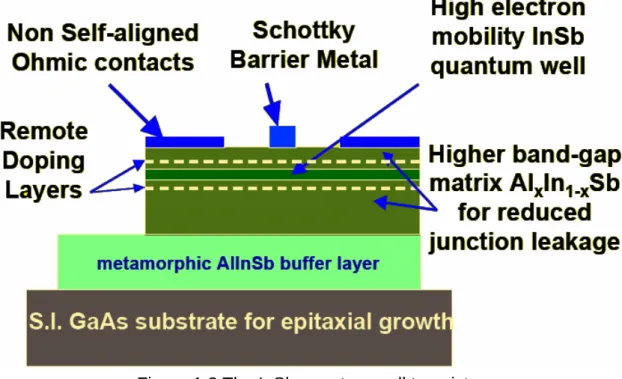
(15) Hk =. h2k 2 2m ∗. (3). The eigenstates for the spin-up condition and the spin-down condition are then E ± (k ) =. h2k 2 ±α k 2m ∗. (4). The amplitude of the spin splitting energy is 2αk F at zero magnetic field at the Fermi energy and is denoted by the notation ∆ R . An electron will precess an amount ∆θ = ω L L v F in traversing a distance L in the quantum well, where ω L = ∆ R m ∗ L h 2 k F . The angle which an electron precesses through in traversing a distance L is. 2m ∗αL ∆θ = h2. (5). The range of values for α given by Nitta et al. [6-7] and Heida et al. [8] is between 0.5 and 1 × 10 −11 eVm, and gives us the corresponding energy splitting 1.5 to 6 meV. Thus, the tunability is achievable through tuning the value of α by an external gate voltage. In addition, Intel also proposed a new generation device which is the “InSb Quantum Well Transistor” recently and was built on the multi-layer epitaxial structure. The structure of the “InSb Quantum Well Transistor” is shown in Figure 1.2. In the structure as you can see in Figure 1.2, the carriers are confined within the InSb quantum well for transport. And we have found some great properties of the material InSb which make it the good candidate for the spintronics application. 6.
(16) Figure 1.2 The InSb quantum well transistor. 7.
(17) It has been recognized that the spin splitting in the asymmetrical quantum well contains two distinct contributions. The first one is due to the inversion asymmetry of the bulk material. The other is the Rashba term which comes from the asymmetry in the macroscopic confining potential. This term has been used to interpret the results of different asymmetric quantum well experiments. It is reasonable for us to believe that this is the term which provides the dominant contribution to the splitting. [1-5] All the examples above tell us that the spintronics will have the weight in the near future. Thus, more knowledge about it is needed in urgent in the spintronics related field either to build the real devices or to continue any deeper research. The asymmetric double well structure which we proposed in this paper provides a configuration to enlarge the spin orbit splitting of the electronic states effectively. Also we demonstrated how the spin-splitting energy will vary with different parameters for any further application in the near future. We will organize this dissertation as several parts. Chapter 1 is the introduction and motivation of our work. Chapter 2 is the basic theories which are concerned in this work. Chapter 3 is the results of our work and will be shown in figures mainly. Chapter 4 is the conclusion of our work.. 8.
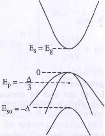
(18) Chapter 2. Theory. 2.1 The k • p method The wave function and the electronic band structure can be derived from the Hamiltonian which satisfies the symmetry of the semiconductor crystal for a periodic potential. Our interest here is near the band edges of the direct band gap semiconductors. The wave vector k deviates by a small amount from a vector c where a local minimum or maximum occurs. The k • p method is a useful technique for us to analyze the band structure which is near a particular point k0 . It will become especially useful when it is near an extremum of the band structure. We consider now the case that the extremum occurs at the zone center where k0 is zero (i.e. the Γ valley). This is a very practical case for III-V direct band gap semiconductor for employed in our work. Consider the general Schrödinger equation for an electron wave function firstly. [. p2 + V (r ) ] Ψnk (r ) = E n (k) Ψnk (r ) 2m0. (6). where Ψnk (r ) is the electron wave function in the nth band with a wave vector k. Next we assume the Block function u nk (r ) is constant over a small region in k-space and rewritten the equation (6). [. h2k 2 p2 h ] u nk (r ) + k ⋅ p + V (r ) ] u nk (r ) =[ E n (k ) − 2m0 2 m0 m0. (7). The above can be expanded near a particular point in the band structure. It will be expanded near E n (0) when k0 =0, 9.
(19) [H 0 +. h2 h2k 2 k ⋅ p ] unk (r ) =[ E n (k ) − ] u nk (r ) m0 2m0. (8). where p2 + V (r ) 2m0. (9). H 0 u n 0 (r ) = E n (0)u n 0 (r ). (10). H0 =. We know that the set of functions u n 0 (r ) forms a complete set of function. Thus, we can employ them to expand the solution at a particular k point. h 2k 2 h h2 E n (k ) = E n (0) + + k ⋅ p nn + 2 2m 0 m0 m0. u nk (r ) = u n 0 (r ) + ∑ [ n' ≠ n. ∑E. n' ≠ n. k ⋅ p nn' n. 2. (0) − E n' (0). (11). k ⋅ p nn ' h ]u ' (r ) m0 E n (0) − E n' (0) n 0. ≡ ∑ a n ' u n ' 0 (r ). (12). Ψnk (r ) = e ik•r u nk (r ). (13). n'. where the momentum matrix elements are defined as. p nn = '. ∫u. ∗ n0. (r )pu n 0 (r )d 3r. (14). (r )u n 0 (r )d 3r = δ nn. (15). '. unit cell. and u nk (r ) ’s are normalized as. ∫u. ∗ n0. '. '. unit cell. If only two strongly interacting nondegenerate bands are considered now, we. 10.
(20) assume. u nk (r ) = ∑ a n ' (k )u n 'o (r ). (16). n'. By substituting equation (16) into equation (8) for u nk (r ) , then multiply by. u n∗0 (r ) and integrate over a unit cell. ∑{[ E. n. (0) +. n'. h2k 2 h ]δ nn' + k ⋅ p nn' } a n = E n (k ) a n 2m0 m0 '. (17). where the orthogonality relation is. ∫u. ∗ n0. (r )u n 0 (r ) d 3r = δ nn '. '. (18). For two coupled bands labeled by n and n’ respectively, the equation (17) can be solved through the determinant equation. E n (0) +. h2k 2 −E 2m0. h k ⋅ p n 'n m0. h k ⋅ p nn' m0 =0 h 2k 2 E n' (0) + −E 2m0. 11. (19).
(21) 2.2 Kane’s model for band structure The spin orbit interaction is taken into account in Kane’s model for direct band semiconductors. The four bands are the conduction band, heavy-hole band, light-hole band, and the spin orbit split-off band respectively. The four bands considered in Kane’s model have double degeneracy with their spin counterparts. The band structure of Kane’s model is shown in Figure 2.1. In other words, Kane’s model is the k • p method with the spin orbit interaction which we need in this work. First, let’s consider the Hamiltonian near the zone center which represents k0 =0. H = H0 +. H0 =. h σ ⋅ ∇V × p 4m02 c 2. p2 + V (r ) 2m0. (20) (21). where the second term in equation (20) represents the spin orbit interaction, σ is the Pauli spin matrix. From the original Schrödinger equation combined with the Bloch function one could obtain,. {[. p2 h + V (r ) + [∇V × p] ⋅ σ } Ψnk (r ) = E n (k) Ψnk (r ) 2m0 4m02 c 2. (22). Then we could obtain the Schrödinger equation for the cell periodic function. u nk (r ). 12.
(22) Figure 2.1 The k • p method in Kane’s model.. 13.
(23) {[. h2 p2 h h + V (r ) + k • p+ + ∇V × k ⋅ σ } u nk (r ) = [ ∇ V × p ] ⋅ σ 2m0 m0 4m02 c 2 4m02 c 2 E ' u nk (r ) (23). where E ' = E n (k ) −. h2k 2 2m0. The fifth term on the left side of equation (23) is a k-dependent spin-orbit interaction. This term is very small compared with the other terms because the crystal momentum hk is very small compared with the atomic momentum p in the far interior of the atom where most of the spin orbit interaction occurs. Thus we could rewrite equation (23) as follows. Hu nk (r ) ≅ ( H 0 +. h h k • p+ [∇V × p] ⋅ σ ) u nk (r ) = E ' u nk (r ) m0 4m02 c 2. (24). The term E ' in equation (24) is the eigenvalue which we look for and which has a corresponding eigenfunction as. u nk (r ) = ∑ a n u n 0 (r ) '. (25). '. n'. The band edge functions u n 0 (r ) are S ↑ and S ↓ the eigenenergy E s for the conduction band, and. which correspond to. X↑. , Y↑ ,. Z↑ ,. X ↓ , Y ↓ , and Z ↓ which correspond to the eigenenergy E p for the 14.
(24) valence band. The wave functions in each band are degenerate with respect to Hamiltonian H 0 . In other words,. H 0 S ↑ = Es S ↑ , H 0 S ↓ = Es S ↓ H0 X ↑ = Ep X ↑ , H0 X ↓ = Ep X ↓ H0 Y ↑ = Ep Y ↑ , H0 Y ↓ = Ep Y ↓ H0 Z ↑ = Ep Z ↑ , H0 Z ↓ = Ep Z ↓. It is convenient to choose the following basis functions since the electron wave functions are p-like near the top of the valence band and s-like near the bottom of the conduction band. The first set of basis functions is degenerate with the second set.. iS ↓ ,. X − iY 2. ↑ , Z↓ , −. X + iY 2. ↑. and. iS ↑ , −. X + iY 2. ↓ , Z↑ ,. X − iY 2. ↓. where. Y10 = Z Y1±1 = m. 1 2. X ± iY. The 8×8 matrix becomes the equation (26) by assuming that the wave vector. k is set along z direction.. 15.
(25) ⎡H 0 ⎤ ⎢ ⎥ ⎢⎣ 0 H⎥⎦. (26). where. 0 ⎡Es ⎢ ∆ ⎢ 0 Ep − 3 ⎢ H= ⎢ 2∆ ⎢kP 3 ⎢ ⎢0 0 ⎣. kP 2∆ 3 Ep 0. ⎤ ⎥ 0 ⎥ ⎥ ⎥ 0 ⎥ ∆⎥ Ep + ⎥ 3⎦ 0. (27). where P is the Kane’s parameter , and Δ is the spin-orbit split-off energy. They are defined as,. h S pz Z m0. P ≡−i. Δ≡ X. Define E p = −. ∂V ∂V py − px Y ∂y ∂x. (28). ∆ and E s = E g to set the proper reference. The top of the 3. valence band for now is zero reference energy. The Hamiltonian thus becomes. ⎡Eg ⎢ ⎢0 H =⎢ ⎢ ⎢ kP ⎢ ⎣0. −. 0. kP. 2∆ 3 2∆ 3 0. 2∆ 3 ∆ − 3 0. 0⎤ ⎥ 0⎥ ⎥ ⎥ 0⎥ ⎥ 0⎦. (29). By equation det H − E ′I =0, we can get the four eigenvalues for E ′ and also. 16.
(26) the corresponding eigenfunctions. For the conduction band,. Ec (k ) = E g +. h 2 k 2 k 2 P 2 (3E g + 2∆) h2k 2 ≡ Eg + + 2m0 3 E g ( E g + ∆) 2me∗. (30). φc ,α = iS ↓. (31). φc , β = iS ↑. (32). 17.
(27) 2.3 The Spin Orbit Interaction The spin orbit interaction is the most important property of the III-V semiconductor materials to be adopted in the spintronics device. This effect comes from the relativistic collection to the non-relativistic electronic Hamiltonian. There are two recognized factors which contribute to the spin-orbit interaction for asymmetric III-V semiconductor quantum wells. The first one is caused by the inversion asymmetry of the zinc blende lattice and is the common modification for III-V semiconductors. The inversion asymmetry will lead to a splitting of conduction band. The energy level of this spin splitting is of the third order of k and is often referred to as the Dresselhaus term. The other one comes from the asymmetry in the macroscopic confining potential and is described by the Rashba term. This term has been used to interpret the results of asymmetric quantum wells and quantum wires successfully. There are also many reasons which make us to believe that this is the most dominant contribution to the spin splitting in the narrow gap heterostructures. To derive the Rashba term, we start from the Kane model. In order to obtain the convenience for the heterostructure problem which has been shown, we choose the following linear combinations as basis functions. [9] u1 = S ↑ ,. 2 Z↑ + 3 1 u3 = − (− iX 2 1 u4 = − [Y ↓ 3 u2 =. 1 6. ( iX ↑ + Y ↓ ) ,. ↑ + Y ↓ ), − ( Z − iX ) ↑ ] ,. u5 = − S ↓ , 18. (33).
(28) 2 Z↓ + 3 1 u7 = − (− iX ↓ 2 1 u8 = − [Y ↑ + 3. u6 = −. 1 6. ( iX ↓ + Y ↑ ) ,. + Y ↑ ), ( Z + iX ) ↓ ] ,. where S , X , Y , and Z denotes the conduction- and the tree-valence bulk Bloch functions at the zone center. The arrows represent the spin state with respect to the y axis. In order to make use of the spherical symmetry of the Kane model, we set the parallel wave vector k along the x axis and the growth direction along the z axis. Then the electron wave function will be given by. 8. ψ (r ) = e ikx ∑ f j ( z )u j (r ). (34). j =1. where f j are the envelope functions. And the effective-mass Hamiltonian can be block diagonalized as. ⎡H + H= ⎢ ⎣0. 0⎤ H − ⎥⎦. (35). with. ⎡ 3 d k V ( z) P[ m ] m Pk ⎢ 2 dz 2 ⎢ ⎢ P[− d m k ] V ( z ) − E 0 g ⎢ 2 dz H± = ⎢ 3 ⎢ m 0 Pk V ( z) − E g 2 ⎢ d ⎢ P 0 0 ⎢ 2 [− dz ± k ] ⎣. 19. ⎤ d ± k] ⎥ 2 dz ⎥ ⎥ 0 ⎥ ⎥ ⎥ 0 ⎥ ⎥ V ( z) − E g − ∆⎥ ⎦ P. [. (36).
(29) where V (z ) is the confining potential, E g is the band gap, ∆ is the spin-orbit energy splitting, and P is the momentum matrix element defined as. P=. 2 h iS p x X 3 me. (37). where me is the bare electron mass. The kinetic energy term is neglected from the diagonal matrix elements because of its relatively small value compared with the off-diagonal elements. By eliminating the other components, we can obtain the equation listed below for the conduction band envelope functions.. [−. 1 d h2k 2 h2 d + + V (z ) m α ( z , ε ± )k − ε ± ] f ± =0 2 dz m( z , ε ± ) dz 2m( z , ε ± ). (38). with. 1 2 1 P2 ] = 2[ + m( z , ε ± ) h ε ± − V ( z ) + E g ε ± − V ( z ) + E g + ∆. (39). and. α ( z, ε ± ) =. 1 1 P2 d [ ] − 2 dz ε ± − V ( z ) + E g ε ± − V ( z ) + E g + ∆. (40). In order to fit the notation parameters which are employed in our structure, we will rewrite equation (38), (39), and (40) as (41), (42), and (43) respectively. The potential profile and the parameters are shown in Figure 2.2.. 20.
(30) Figure 2.2 The potential profile of the asymmetric double well structure. 21.
(31) [−. 1 d h2k 2 h2 d dβ + + Ec (z ) + V (z ) m ( ( z , ε ± ))k − ε ± ] f ± =0 2 dz m( z , ε ± ) dz 2m( z , ε ± ) dz. (41). 1 2 1 P2 ] = 2[ + m( z , ε ± ) h ε ± − V ( z ) − E v ( z ) ε ± − V ( z ) − E v ( z ) + ∆ ( z ). (42). 1 1 P2 [ ] − 2 ε ± − V ( z ) − Ev ( z ) ε ± − V ( z ) − Ev ( z ) + ∆( z ). (43). with. and. β ( z, ε ± ) =. The ± sign in the equations above refers respectively to spin up and spin down along the y direction. The term β is the spin coupling parameter. Now let us discuss the boundary conditions in the calculation. Firstly we consider the case at z = 0 an interface between two semi-infinite layers of semiconductors 1 and 2. And we may write this as. 1 1 1 = θ (− z ) + θ ( z) m m1 m2. (44). β = β1θ (− z ) + β 2θ ( z ). (45). and. By integrating across the interface, we can obtain boundary conditions as. f ± continuous. (46). h 2 df ± m βkf ± continuous 2m dz. (47). and −. The two-spin components are always decoupled. The basis functions for the 22.
(32) spin states are those which point along the y direction. If we denote Ψ as the spinor with components f + and f − , the boundary conditions can be written as. Ψ continuous. (48). h2 d Ψ + σ y β kΨ continuous 2m dz. (49). and. where σ y is the Pauli spin matrix. This is the simpler form which shows the cross product symmetry in the Rashba term. Because we set the spin quantization direction along the. k-dependent effective magnetic field, the decoupling of the spins and the consequent simplicity in the expressions listed above occur. If k or Δ goes to zero, the boundary conditions above will reduce to the generalized Ben Daniel-Duke boundary conditions. Also, in the case of symmetric quantum wells, the Rashba splitting is exactly zero because of the mirror reflection which will take the spin-up condition into the spin-down condition and vice versa. By considering the dependence of β on z in equation (41), and thereby two contributions to the Rashba spin-orbit splitting are distinguishable. The first one is the discontinuity of the band parameters, while the second one is related to the space charge and/or the external electrostatic field. The discontinuity of the band parameters will set the spin dependent boundary conditions, while the external electric field gives a spin dependent term in the effective mass Hamiltonian. These two contributions to the Rashba term have been identified in a previous estimation of the Rashba coupling parameter. [10] 23.
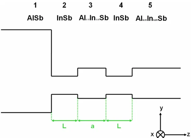
(33) Chapter 3. Results. 3.1 Asymmetrical Square Double Well The discontinuities of the band parameters and the space charge and/or the external electrostatic potential would contribute to the Rashba term in a similar way only if the band edge discontinuities were all the same. But the two contributions are of a different character and are both presented in the real sample. Let us first consider the problem of the bound states of the electrons which are confined in the semiconductor double well structure of the type. Al x In 1-x Sb/InSb/Al y In 1- y Sb/InSb/Al y In 1- y Sb with x ≠ y . The potential profile is shown in the Figure 3.1. By solving equation (41) we can obtain the eigenvalues ε ± for each value of k . We set the wave functions as. ϕ1 = C1e q z l. ϕ 2 = C 2 cos(k w z ) + C3 sin(k w z ) ϕ 3 = C 4 e q z + C5 e − q z r. r. ϕ 4 = C 6 cos(k w z ) + C 7 sin(k w z ) ϕ 5 = C8 e − q z. (50). r. The wave vectors in the growth direction are given by. ql =. 2ml ( Ec ,l − ε ) + k 2 h2. (51). kw =. 2mw (ε − Ec , w ) − k 2 h2. (52). 24.
(34) Figure 3.1 The potential profile of Al x In1- x Sb/InSb/Al y In1- ySb/InSb/Al y In1- ySb asymmetric double well. 25.
(35) qr =. where. l. 2mr ( Ec , r − ε ) + k 2 h2. denotes the barrier of the region 1.. region 2 and 4.. (53). w. denotes the wells in the. denotes the barrier in the region 3 and 5.. r. By the boundary conditions from equations (46) and (47), we can get. ϕ1 = ϕ 2 −. h2 h2 ∂ zϕ1 + β1kϕ1 = − ∂ zϕ 2 + β w kϕ2 2ml 2mw. ϕ2 = ϕ3 −. z=L. z=L. (54). z =a+ L. h2 h2 ∂ zϕ3 + β r kϕ3 = − ∂ zϕ4 + β wkϕ4 2mr 2mw. ϕ4 = ϕ5 −. z =0. h2 h2 ∂ zϕ2 + β wkϕ2 = − ∂ zϕ3 + β r kϕ3 2mw 2mr. ϕ3 = ϕ 4 −. z =0. z =a + L. z =a+2 L. h2 h2 ∂ zϕ4 + β wkϕ4 = − ∂ zϕ5 + β r kϕ5 2mw 2mr. z =a + 2 L. Next we write down the plane wave solutions for ϕ i in the different regions which match the boundary conditions at the interfaces. The solutions are. 26.
(36) (−1+ e 2aqr )⟨ml {mr [h 4 kw2 + 4k 2 mw2 (βl − β w )(β r − β w )]+ 2h 2 kqr mw2 (βl − β w )}+ h 2 ql mw2 [h 2 qr + 2kmr (β r − β w )]⟩{h 4 qr2 mw2 + mr2 [h 4 kw2 + 4k 2 mw2 (β r − β w ) 2 ]. + 4h 2 kqr mr mw2 (−β r + β w )}+ 2 eaqr cos(2kw L) 2h6 kw2 qr cosh(aqr )mr mw2 {h 2 ql mr + ml [h 2 qr + 2kmr (βl − βr )]}− sinh(aqr ){−h 4 qr2 mw2 + mr2 [h 4 kw2 + 4k 2 mw2 (βr − β w ) 2 ]}. ⟨ml {mr [h 4 kw2 + 4k 2 mw2 (βl − β w )(βr − β w )]+. (55). 2h kqr m (−βl + β w )}− h ql m [h qr + 2kmr (−βr + β w )]⟩ = 2. 2 w. 2. 2 w. 2. 2 e2aqr h 2 kw sin(2kw L)mw sinh(aqr ){h 2 ql mr + ml [h 2 qr + 2kmr (βl − β r )]} {−h 4 qr2 mw2 + mr2 [h 4 kw2 + 4k 2 mw2 (β r − β w ) 2 ]}+ 2h 2 qr cosh(aqr )mr. ⟨ml {mr [h 4 kw2 + 4k 2 mw2 (βl − β w )(β r − β w )]+ 2h 2 kqr mw2 (−βl + β w )}− h 2 ql mw2 [h 2 qr + 2kmr (−β r + β w )]⟩. And mi and β i could be obtained by equation (42) and (43) respectively. L is the well width in region 2 and 4. a is the barrier width in region 3. ε ± is. the energy which satisfies equation (55) with ± β i .. 27.
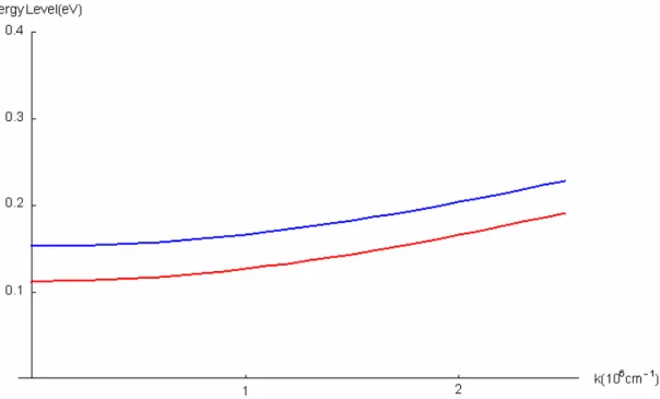
(37) 3.2 The Energy Levels and Spin Splitting in the Asymmetric Double Well Structure Consider the case x =1, y = 0.15 as shown in Figure 3.2. Then we will obtain an AlSb/InSb/Al 0.15 In 0.85Sb/InSb/Al0.15 In 0.85Sb asymmetric double well structure. In this structure, we set the well width L in region 2 and region 4 as 5 nm and the barrier width a in region 3 as 5 nm initially. For AlSb , the energy gap is 2.384 eV, Δ is 0.673 eV, and the effective mass is 0.26m0 . For InSb , the energy gap is 0.2352 eV, Δ is 0.81 eV, and the effective mass is. 0.01359m0 . For the conduction band offset, we adopt the 72% rule. Then we can obtain the barrier height V1 at the AlSb/InSb interface as 1.547 eV, and the barrier height V2 at the InSb/Al0.15 In 0.85 Sb interface as 0.232 eV respectively. In Figure 3.3, we plot the energy levels of this structure as a function of k . We can see that there are two energy levels exist in this well, but we can not obtain any further information through this plot. For more information, we need the plot of the spin splitting of the energy levels as shown in Figure 3.4. We can see clearly the splitting of the energy levels increases with in-plane wave vector k in Figure 3.4. Thus we can confirm the spin splitting of the asymmetric double well does exist and needs further exploration from us. We will demonstrate some configurations which can alter the characteristic of this asymmetric double well structure to see how the spin splitting of energy will vary with different variables in the following sections.. 28.
(38) Figure 3.2 The potential profile of AlSb /InSb/Al0.15 In 0.85 Sb/InSb/Al0.15 In 0.85Sb asymmetric double well. 29.
(39) Figure 3.3 The energy levels in AlSb /InSb/Al0.15 In 0.85 Sb/InSb/Al0.15 In 0.85Sb asymmetric double well with respect to in-plane wave vector. 30.
(40) Figure 3.4 The spin splitting of energy in. AlSb /InSb/Al0.15 In 0.85Sb/InSb/Al0.15 In 0.85 Sb asymmetric double well with respect to in-plane wave vector. 31.
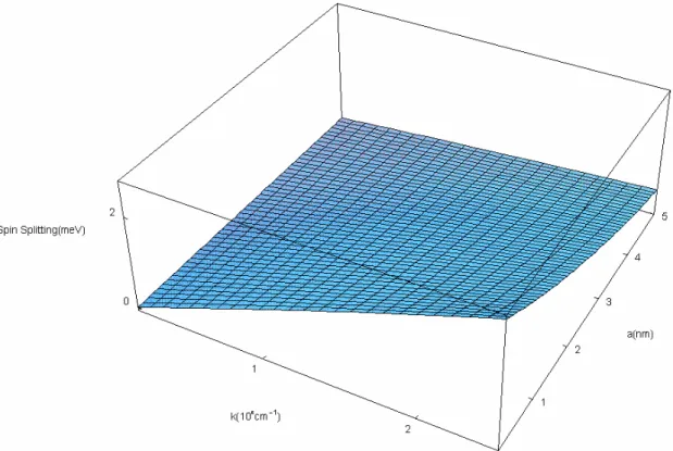
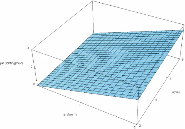
(41) 3.3 The Variation of the Barrier Width in the Asymmetric Double Well In this case, we set the well width in region 2 and 4 as 5nm, x as 1, and y as 0.15 to see how the spin splitting will behave with different values of the wave vector k and the barrier width a . With x is 1, and y is 0.15, we could obtain the structure AlSb/InSb/Al 0.15 In 0.85Sb/InSb/Al0.15 In 0.85Sb . The potential profile of this case is the same as Figure 3.2. Figure 3.5 is the plot of the spin splitting of the ground state with respect to k and a . Figure 3.6 is the plot of the spin splitting of the first excited state with respect to k and a . In Figure 3.5, we can clearly see that the amplitude of the spin splitting decreases with the increase of the barrier width a , while it increases with the increase of the in-plane wave vector k . We also show the variation caused by different value of the mole fraction x for the ground state and the first excited state in Figure 3.7 and Figure 3.8 respectively.. 32.
(42) Figure 3.5 The spin splitting of the ground state in. AlSb /InSb/Al0.15 In 0.85Sb/InSb/Al0.15 In 0.85 Sb asymmetric double well with respect to the in-plane wave vector k and the barrier width a. 33.
(43) Figure 3.6 The spin splitting of the first excited state in. AlSb /InSb/Al0.15 In 0.85Sb/InSb/Al0.15 In 0.85 Sb asymmetric double well with respect to the in-plane wave vector k and the barrier width a. 34.
(44) Figure 3.7 The spin splitting of the ground state in. AlSb/InSb/Al x In 1− x Sb/InSb/Al x In 1− x Sb asymmetric double well with respect to the in-plane wave vector k and the mole fraction x. 35.
(45) Figure 3.8 The spin splitting of the first excited state in. AlSb/InSb/Al x In 1− x Sb/InSb/Al x In 1− x Sb asymmetric double well with respect to the in-plane wave vector k and the mole fraction x. 36.
(46) 3.4 The Variation of the Barrier Height in the Asymmetric Double Well In addition to the variation of the barrier width in the asymmetric double well structure, one can also modify the barrier height of the barrier to control the spin splitting of energy.. In this structure, the well width and the barrier width are both set as 5nm. The mole fraction x is 1 while the mole fraction y is 0.15, and which provide us the double quantum well structure of. AlSb/InSb/Al 0.15 In 0.85Sb/InSb/Al 0.15 In 0.85Sb . And the term ∆V is the increment of the barrier height. The band structure for this case is shown in Figure 3.9. Note that the effective mass m3 and the spin coupling parameter β 3 for region 3 are concerned with the parameter ∆V since it will change the conduction band edge of this region as a consequence. With the same procedure which had been mentioned in section 3.1, we could obtain the dispersion relation for this case. sinh(aq3 )m32 ⟨− h 2 k w cos(k w L)m w [h 2 ql + 2kml (− β 3 + β l )] + sin(k w L){ml [h 4 k w2 + 4k 2 m w2 ( β 3 − β w )( β l − β w )] + 2h 2 kql m w2 ( β 3 − β w )}⟩ ⟨− h 2 k w cos(k w L)m w [h 2 q r + 2kmr ( β 3 − β r )] + sin(k w L) {mr [h 4 k w2 + 4k 2 m w2 ( β 3 − β w )( β r − β w )] + 2h 2 kq r m w2 (− β 3 + β w )}⟩ + h 4 q32 sinh(aq3 )m w2 {h 2 k w cos(k w L)ml + sin(k w L)m w [h 2 ql + 2kml ( β l − β w )]} {h 2 k w cos(k w L)mr + sin(k w L)m w [h 2 q r + 2kmr (− β r + β w )]} + h 2 k w q3 cosh(aq3 )m3 m w h k w cos(k w L)m w {h 2 ql mr + ml [h 2 q r + 2kmr ( β l − β r )]} + 2. sin(2k w L)⟨ h 2 ql m w2 [h 2 q r + 2kmr (− β r + β w )] + ml {2h 2 kq r m w2 ( β l − β w ) + mr [−h 4 k w2 + 4k 2 m w2 ( β l − β w )(− β r + β w )]}⟩ = 0. 37. (56).
(47) Figure 3.9 The potential profile of AlSb /InSb/Al 0.15 In 0.85Sb/InSb/Al 0.15 In 0.85Sb asymmetric double well with the barrier height changed by the amount ΔV. 38.
(48) In Figure 3.10, we plot the spin splitting with a fixed in-plane wave vector. k = 2 × 10 6 cm −1 as a function of the barrier width and the increment of the barrier height. In this figure, the large spin splitting could be obtained even when the parameter ∆V is zero. We had already shown how the splitting varies with the barrier width in section 3.3. However this is the less elastic way to control the splitting since it relates to the process mainly and are fixed initially. But we can still enlarge the amplitude of the splitting by applying the external voltage which will modify the barrier height. Obviously this use can provide people more flexibility to correlate this effect with any further application.. 39.
(49) Figure 3.10 The spin splitting of energy in. AlSb /InSb/Al 0.15 In 0.85Sb/InSb/Al 0.15 In 0.85Sb asymmetric double well with respect to the barrier width a and ΔV. 40.
(50) Chapter 4. Conclusion. The most structures or theories for the spintroics are based on the metal or the dielectric materials only. But our proposal here attempts to realize the spin splitting mechanism in the total semiconductor structure. This will provide us the convenience of both the easier operation and the massive production as a consequence. In this research we have presented a theoretical study of the spin orbit splitting in energetic levels in asymmetric double well structure and demonstrated some configurations which enlarge the amplitude of the spin splitting effectively. We began with the energy levels and the spin splitting which exist in the well. After that, we organized some achievable and effective configurations to control the spin splitting and observed how spin splitting behaves with different factors. To control it as we wish in real applications, there are two essentials which we need. The first one is the large amplitude of the spin splitting. And the second is that this effect must be controllable. No lack of the two essentials described above at the same time is the only way to make sure this mechanism can function as well as we wish since the energy levels at the stage right now are on the electron volt scale. Our research is the first step for this application and can be the starting point for the more detailed calculation. More experimental results are required to confirm the results in this research further.. 41.
(51) References [1] J. Luo, H.Munekata, F. F. Fang, and P. J. Stiles, Phys. Rev. B 41, 7685 (1990) [2] B. Das, D. C. Miller, S. Datta, R. Reifenberger, W. P. Hong, P. K. Bhattacharya, J. Singh, and M. Jaffe, Phys. Rev. B 39, 1411 (1989) [3] S. K. Greene, J. Singleton, P. Sobkowicz, T. D. Golding, M. Paper, J. A. Parenboom, and J. Dinan, Semicond. Sci. Technol. 7 1377 (1992) [4] F. Malcher, G. Lomer, and U. Rössler, Superlatt. Microstruct. 2, 267 (1986) [5] E. A. de Andrada e Silva, G. C. La Rocca, and F. Bassani, Phys. Rev. B 50, 8523 (1994) [6] J. Nitta, T. Akazaki, H. Takayanagi, Phys, Rev. Lett. 78, 1335 (1997) [7] C. M. Hu, J. Nitta, T. Akazaki, H. Takayanagi, Phys, Rev. B 60, 7736 (1999) [8] J. P. Heida, B. J. van Wees, J. J. Kuipers, T. M. Klapwijk, Phys. Rev. B 57, 11911 (1998) [9] E. A. de Andrada e Silva, G. C. La Rocca and F. Bassani, Phys. Rev. B 24, 16 293 (1997) [10] A. Voskoboynikov, Shiue Shin Liu and C. P. Lee, Phys. Rev. B 58, 15 397 (1998) [11] G. Dresselhaus, Phys. Rev. 100, 580 (1955) [12] Supriyo Datta and Biswajit Das, Appl. Phys. Lett. 56, 665 (7) (1990) [13] Yu. A. Bychkov and E. I. Rashba, J. Phys. C 17, 6039 (1984) [14] O. E. Raichev and P. Debray, Phys, Rev. B 67, 155304 (2003) [15] G. Bastard, Wave Mechanics Applied to Semiconductor Heterostructures (Les Edition de Physique, Les Ulis, 1990) [16] Shun Lien Chuang, Physics of Optoelectronic Devices (Wiley-Interscience,.
(52) New York, 1995) [17] D. D. Awschalom, D. Loss, and N. Smarth (Eds.), Semiconductor Spintronics and Quantum Computation (Springer, 2002) [18] Suman Datta and Robert Chau Intel Corporation, USA, Novel InSb-based Quantum Well Transistors for Ultra-High Speed, Low Power Logic Applications (2005).
(53) Vita 姓名 : 陳啟暉 出生年月日 : 民國 66 年 7 月 27 日 籍貫 : 台灣省台南縣 學歷 : 國立台灣科技大學電子工程系 (89.9-91.6) 國立交通大學電子工程研究所碩士班 (92.9-94.6) 碩士論文題目 : 半導體非對稱雙量子井結構中之自旋相依能階分裂 Spin Orbit Splitting of Energy Levels in Semiconductor Asymmetric Double Well Structure.
(54)
數據
+7

Outline
相關文件
INFORMAÇÃO GLOBAL SOBRE AS ASSOCIAÇÕES DE SOLIDARIEDADE SOCIAL E OS SERVIÇOS SUBSIDIADOS REGULARMENTE PELO INSTITUTO DE ACÇÃO SOCIAL. STATISTICS ON SOCIAL SOLIDARITY ASSOCIATIONS
Valor acrescentado bruto : Receitas do jogo e dos serviços relacionados menos compras de bens e serviços para venda, menos comissões pagas menos despesas de
Valor acrescentado bruto : Receitas do jogo e dos serviços relacionados menos compras de bens e serviços para venda, menos comissões pagas menos despesas de
投票記錄:核准 3 票、修正後核准 10 票、修正後複審 0 票、不核准 0 票、棄權 0 票。.. 審查結果:修正後核准(追蹤審查頻率為半年一次) 。
6 《中論·觀因緣品》,《佛藏要籍選刊》第 9 冊,上海古籍出版社 1994 年版,第 1
(In Section 7.5 we will be able to use Newton's Law of Cooling to find an equation for T as a function of time.) By measuring the slope of the tangent, estimate the rate of change
Robinson Crusoe is an Englishman from the 1) t_______ of York in the seventeenth century, the youngest son of a merchant of German origin. This trip is financially successful,
fostering independent application of reading strategies Strategy 7: Provide opportunities for students to track, reflect on, and share their learning progress (destination). •
