利用齊納接面改善氧化矽/氮化矽/氧化矽
堆疊式快閃記憶體之特性
學生: 梁 文 彥
指導教授: 雷 添 福
博 士
國立交通大學
電子工程學系
電子研究所碩士班
摘
要
目前論文的題目主要是以探討在現今被廣泛使用的浮動閘極(Floating Gate)非揮發性記憶體。就快閃記憶體而言,通常會遇到兩個問題:首先是在元 件的穿隧氧化層厚度小於 10 奈米時,雖可改善快閃記憶體的讀寫速度,但電荷 保存時間亦隨之下降。再來是經過多次讀寫後在穿隧氧化層品質容易劣化而產生 漏電路徑,而一旦有一條漏電路徑產生,所有儲存在浮動閘極的電荷都會經由此 漏電路徑而全部流失掉,這也是目前浮動閘極非揮發性記憶體最嚴重的問題。 氧化矽/氮化矽/氧化矽堆疊式(SONOS)結構的記憶體元件,是使用氮化矽 作為電荷陷捕層,在此種結構內,因為電荷是被儲存在分離式的陷捕位置中,故 可改善在浮動閘極結構中對於資料保存性的問題。但是因為氮化矽與穿隧氧化層 之間的導電帶位能差太低,會使得元件的寫入/抹除(program/erase)速度降低, 而現在記憶體的基本要求不外乎在加快寫入/抹除的速度,增加資料保存的期限 (retention),在連續的寫入/抹除的重複性動作下,去提升元件對此動作的忍 受度(endurance)。 而在本篇論文中,我們將在源極(source)端和汲極(drain)端形成一個 齊納接面(Zener junction),利用齊納接面(Zener junction)的特性去改善 傳統氧化矽/氮化矽/氧化矽堆疊式快閃記憶體(SONOS)的寫入及抹除的特性。在本篇論文的第二章中,首先探討不同條件的齊納接面對 P 型基板之 SONOS 記憶體元件的寫入及抹除速度帶來的影響,並且進一步觀察此齊納接面是否對元 件其他的特性有負面影響,並分析元件特性的原理。
在本篇論文的第三章中,探討不同條件的齊納皆面對 N 型基板之 SONOS 記憶 體元件的寫入及抹除速度產生的影響,並同時觀察記憶體其他特性,受到齊納接 面結構影響後,是改善或者劣化,最後會分析元件特性的原理。
在本篇論文的第四章中,會做一個簡單的結論,比較 n-channel 和 p-channel 之間的優缺點。
Study on SONOS Flash Memory with
Zener Junction at Source/Drain Side
Student : Weng-yeng Liang
Advisor : Dr. Tan-Fu Lei
Department of Electronics Engineering &
Institute of Electronics
National Chiao Tung University
ABSTRACT
The topic of the paper is the floating gate non-volatile flash memory which is extensively used in the present. For the non-volatile flash memory, there are two problems: First, when the thickness of tunneling oxide is scaled down to 10 nano-meter, the programming speed of flash memory is improved, but the retention time is decreased. Second, after the programming and erasing operation cycles, it will cause the tunneling oxide damage and make the oxide quality degradation. The oxide damage would generate a leakage path which will cause the charges stored in
floating-gate layer lost by the leakage path. The leakage issue is the most serious problem of the floating-gate non-volatile flash memory.
In order to solve the leakage path problem, we use the
silicon-oxide/silicon-nitride/silicon-oxide stack structure memory device. The
silicon-nitride layer is used to be the charge trapping layer. Because the charge stored in the trapping is in the discrete trapping site in the stack structure device, it can improve the data retention reliability compared with the floating-gate flash memory. Because of the difference of conduction band between silicon-nitride trapping layer
and silicon-oxide tunneling layer is too small, the programming speed and the erasing speed of the stack structure will decrease. But the operation speed, well data retention reliability, and the endurance of the device under the stress by the repeated program and erase cycles in the memory device are the most important requirements.
In the thesis, we will form a Zener junction at the source side and the drain side, then we employ the Zener junction to improve the program and erase characteristic of SONOS stack structure memory.
In the Chapter 2, we will use the different dose of boron doping to perform the reverse halo implantation. Then we would discuss the effect on the programming speed and the erasing speed of P-type substrate SONOS memory with the different condition of the Zener junction. Finally, we will observe if the Zener junction caused the degradation on the other characteristics of memory, and explain these
phenomenons further.
In the Chapter 3, we will talk about the effects on the characteristics of the n-type substrate SONOS memory , especially on the programming and erasing speed. We use the different does of phosphorus doping to accomplish the reverse halo implantation. And we would observe the characteristics of SONOS memory such as programming speed, erasing speed, data retention, endurance, and so on. Finally, we will find the theorem to explain the phenomenon. At last, we will give an conclusion in Chapter 4.
誌謝
首先在此要向我的指導教授雷添福博士至上最高的敬意。感謝他在學業、研 究與生活上給予的指導與鼓勵。在兩年的碩士求學階段,讓我學習到應有的學習 態度與方法,令我受益匪淺。 感謝俊嘉學長,在實驗的過程中,只要學弟需要你的幫忙,你總是鼎力相助, 不論自己有多忙;在量測與分析階段,自己要準備考試和處理很多瑣事,還是不 厭其煩的指導與幫忙,否則我的碩士論文沒有辦法這麼順利的完成。另外也要感 謝家文學長,會適時的給予意見和幫忙,常會帶著我們去從事課業以外的活動。 還有志仰學長、錦石學長、任逸學長、源竣學長提供在課業和生活上的寶貴經驗。 還有常常回來實驗室的余博、alen、久騰、文瑋、小王子,謝謝你們為實驗室帶 來歡樂。 再來要感謝在實驗室一同奮鬥的伙伴,小 P、羅大、子恒、冠良、敬為、景 琳、伊容學姐和春瑀,在實驗和課業上,有大家的幫忙,讓我能克服種種困難; 在生活上,有大家提供的歡笑,為枯燥乏味的生活增添許多色彩,讓我開心的度 過兩年的碩班生活。也要謝謝所有在交大的好朋友們,佳樺、夏猪、信富、元愷、 土豆、修哥、阿邦,謝謝在我身旁的所有朋友,在我需要幫助時,總是不吝嗇的 伸出援手,謝謝大家。 最後,我要感謝我的爸爸、媽媽、姊姊和阿姨,在我的求學之路有他們的不 求回報的全力支持,我才能夠無後顧之憂的完成我的學業,爸爸、媽媽、姊姊、 阿姨謝謝你們!!還有陪伴我一路走完碩士生涯的佑珊,在我心情低落的時候, 總是替我打氣、幫我分憂,謝謝妳!!僅此論文獻給我的家人、佑珊及所有關心 我的朋友們。Contents
Abstract (Chinese)... I Abstract (English)... III Acknowledge... V Contents………..VI Table & Figure Captions………...IX
Chapter 1 Introduction………...1
1-1 Overview of Flash Memory...1
1-2 Motivation...3
1-3 Thesis Organization...4
1-4 Reference...9
Chapter 2 Characteristic of N-Channel SONOS Memory with Zener Junction at S/D Side...11
2-1 Introduction...11
2-2 Experimental...12
2-3 Results and Discussion...22
2-3-1 Id-Vg Curve…...22
2-3-2 Program and Erase Speed...25
2-3-3 Data Retention Characteristics...33
2-3-4 Disturbance Measurement...36
2-3-5 Endurance Characteristics...39
2-4 Summary...41
2-5 Reference...42
Chapter 3 Characteristic of P-Channel SONOS Memory with Zener Junction at S/D Side...43
3-1 Introduction...43
3-2 Experimental...47
3-3 Results and Discussion...55
3-3-1 Id-Vg Curve…...55
3-3-2 Program and Erase Speed...57
3-3-3 Data Retention Characteristics...61
3-3-4 Disturbance Measurement...62
3-3-5 Endurance Characteristics...64
3-4 Summary...67
3-5 Reference...68
TABLE CAPTIONS
Chapter 2
Table 2-1 Split Table of Implantation in n-channel SONOS memory……….21
Chapter 3
FIGURE CAPTIONS
Chapter 1
Fig. 1-1 The applications of flash memory…………...……….5
Fig. 1-2 The semiconductor memory……….5
Fig. 1-3 Structure of floating gate memory………6
Fig. 1-4 Leakage paths induce all charge lost in the floating gate……….……6
Fig 1-5 Structure of SONOS memory………7
Fig. 1-6 Leakage paths induce partial charge lost in the Nitride trapping layer………7
Fig 1-7 The Id-Vg curve the flash memory ………...8
Chapter 2
Fig. 2-1 Process flow of the Zener junction SONOS memory………...14-20 Fig. 2-2 Id-Vg curve of the conventional device……….23Fig. 2-3 Id-Vg curve of the Zener device……….23
Fig. 2-4 Channel hot electron injection (CHE) programming mechanism ………….24
Fig .2-5 Band to band hot hole (BBHH) erasing mechanism………..24
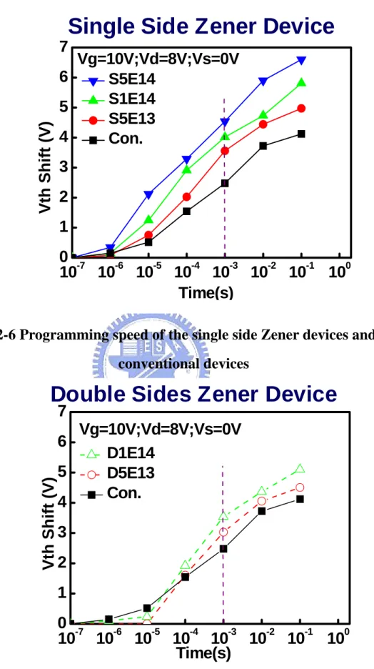
Fig. 2-6 Programming speed of the single side Zener device and the conventional device……….26
Fig. 2-7 Programming speed of the double side Zener device and the conventional device……….26
Fig. 2-8 Tunneling oxide band diagram at programming state………27
Fig. 2-9 Programming speed comparison of the single side Zener device and the double sides Zener device………. ……...28
Fig. 2-10 Band diagram comparison between the single side device and the double sides Zener device at Source side………...…….29
Fig. 2-11 Erasing speed of the single side Zener device and the convention device………...30
Fig. 2-12 Erasing speed of the double sides Zener device and the convention
eviced……….……..30
Fig. 2-13 Erasing speed of the single side Zener device and the double sides Zener device………. ……….31
Fig. 2-14 Junction band diagram at erasing state……….32
Fig. 2-15 Data retention characteristic of the single side Zener device and the conventional device………...………. ……….34
Fig. 2-16 Data retention compared with the double sides Zener device and the conventional device.………..……….…………. …34
Fig. 2-17 Charge stored location in the single side Zener device………35
Fig. 2-18 Charge stored location in the double sides Zener device……….…………35
Fig. 2-19 Drain disturbance as the memory device at programming state……..……36
Fig. 2-20 Drain disturbance between the single side Zener device and the conventional device at Vd = 8V……….………..37
Fig. 2-21 Drain disturbance between the double sides Zener device and the conventional device at Vd = 8V………...37
Fig. 2-22 Drain disturbance between the single side Zener device and the conventional device at Vd = 10V……….38
Fig. 2-23 Drain disturbance between the double sides Zener device and the conventional device at Vd = 10V……….38
Fig. 2-24 Endurance characteristic of the conventional device………39
Fig. 2-25 Endurance characteristic of the single side Zener device……….40
Fig. 2-26 Endurance characteristic of the double sides Zener device………..40
Chapter 3
Fig. 3-1 Band to band hot hole induced hot electron programming mechanism…….45Fig. 3-3 Drain side FN erasing mechanism………46 Fig. 3-4 Process flow of the Zener junction SONOS memory……….………….49-53 Fig .3-5 Id-Vg curve of the conventional device………56 Fig. 3-6 Id-Vg curve of the Zener device………56 Fig. 3-7 Programming speed of the Zener device and the conventional device……..57 Fig. 3-8 Tunneling oxide band diagram at programming state………58 Fig. 3-9 Erasing speed of the Zener device and the convention device………...59 Fig. 3-10 Junction band diagram at erasing state……….60 Fig. 3-11 Data retention characteristic of the Zener device and the conventional
device………..……….61 Fig. 3-12 Drain disturbance as the memory device at erasing state……….62 Fig. 3-13 Drain disturbance between the Zener device and the conventional device at
Vd = -8V………..63 Fig. 3-14 Drain disturbance between the Zener device and the conventional device at
Vd = -10V………63 Fig. 3-15 Endurance characteristic of the conventional device………...65 Fig. 3-16 Endurance characteristic of the Zener device………...65 Fig. 3-17 Charge injection region in the P-channel memory as programming and
CHAPTER 1
INTRODUCTION
1.1 Overview of Flash Memory
Because of the memory devices used in the currently 3C products widely, such as mobile capabilities, Personal Digital Assistant (PDA), Digital Camera, computer, and some other electric consumer products, as figure 1-1 shows. Hence the memory device technology is developing rapidly in present.
The semiconductor memories based on complementary CMOS
(metal-oxide-semiconductor) technology can be divided into two main parts by whether the storage data can be kept without power supply. If the memory devices can not keep the data without power supply, we call these memory devices as the volatile memory. And the other memory devices can keep data without power supply called the
non-volatile memory. The volatile memory: like static random access memory (SRAM) and dynamic random access memory (DRAM). The non-volatile memory: like
electrically programmable read only memory (EPROM), electrically erasable
programmable read only memory (EEPROM), and the flash memory. We show them in figure 1-2.
The most explosive growth field of the semiconductor is the flash memory. The advantages of the flash memory are that it can be electrically written and erased more than 100k times with byte programming and sector erasing and being with the smallest cell size [1]-[2].
In 1967, the first floating gate non-volatile semiconductor memory was invented by S. M. Sze and D. Kahng at Bell Labs [3]. The conventional floating gate memory used poly-silicon as a charge storage layer surrounded by the dielectric [1], as figure 1-3.
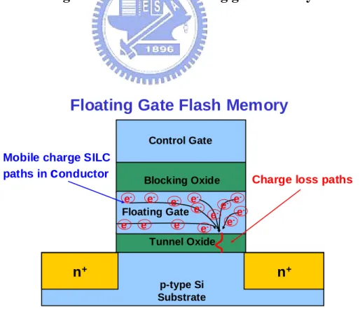
good reliability for flash memory application. But the floating gate memory meets the limitation of scaling down. When the tunneling oxide thickness was scaled down to 10nm, the charge stored in the poly-silicon floating gate would be easy to leak by a leakage path of the tunneling oxide or direct tunneling current, as figure 1-4. The reason of the leakage path forming is that some defect would generate during repeated
write/erase cycles.
In order to reach higher cell density, the scaling down issue of the memory devices is unavoidable. First, we must solve the leakage problem of the floating gate memory with the thickness of the tunneling oxide thinner than 10nm. The SONOS
(Poly-silicon/Oxide/Nitride/Oxide/Silicon) stack structure flash memory has been invented to solve the issue of the floating gate memory recently. SONOS memory has better charge retention ability than the floating gate memory when the tunneling oxide thickness reduced [4]-[5]. Because that the trapping sites in the nitride trapping layer are spatially isolated deep-level traps. Hence, a single leakage path in the tunneling oxide will not induce the whole charges in trapping layer lost [6], as figure 1-6. The structure of SONOS memory is depicted in Fig 1-5. The Id-Vg curve characteristic of the flash memory is shown in Fig 1-7 [7]. The shift of threshold voltage between program state and erase state is named memory window.
The SONOS memory solves the leakage path issue and has several advantages including fast programming, low power operation, high-density integration, and good endurance characteristics [8]-[11], but the retention characteristics of the SONOS memory are not good enough. Because the trapping sites in the nitride trapping layer of the SONOS memory are shallower trapping level. Hence, we need to make tunneling oxide and blocking oxide thicker, but it will decrease the operation speed [12]-[15]. To improve the programming and erasing speed of the SONOS memory with well retention characteristics is one of the most popular topics in the research today. There are many
ways to improve the programming and erasing speed without retention degradation, such as using high-k dielectric as tunneling oxide [16]-[18]. When we apply a voltage on memory device, the partial voltage on the tunneling oxide is larger. Then, we can enlarge tunneling oxide energy band bending to increase programming and erasing speed. But the high-k material has some new troubles, like the compatibility to the process flow today, the stability under high temperature process environment, and so on. Here, we do not use the high-k material to improve the programming and erasing speed of the SONOS memory. Instead of the high-k material techniques is using heavily reverse type halo-implantation to from the Zener junction by the side of the drain in the channel.
1.2 Motivation
When the problem of the leakage path inducing charge stored in the floating gate memory lost was solved by the SONOS stack structure memory, the new problem of the SONOS memory is coming together. The discrete trapping site solved the charge lost issue in the floating gate memory, but it also caused the programming and erasing speed degradation at the same time. And the high-k material still has some troubles, like the compatibility to the process flow today, the stability under high temperature process environment. Hence, we use the reverse halo-implantation forming the Zener junction in the thesis to improve the programming and erasing speed without using high-k material. Using this method will not meet the problems of high-k material. Especially, we do not need add any more exposure and develop process steps to complement the reverse halo-implantation because it can be done in sequent process step with the source/drain implantation. By the reason, we don’t need one more masks, and the cost won’t add.
1.3 Thesis Organization
In this thesis, we study the performance of the SONOS stack structure memory device used the Zener junction to improve the programming and erasing speed.
In the Chapter 2, we will use the different dose of boron doping to perform the reverse halo implantation. Then we would discuss the effect on the programming speed and the erasing speed of P-type substrate SONOS memory with the different condition of the Zener junction. Finally, we will observe whether the Zener junction causing the degradation on the other characteristics of memory, and explain these phenomenon further.
In the Chapter 3, we will talk about the effects on the characteristics of the n-type substrate SONOS memory, especially on the programming and erasing speed. We use the different does of phosphorus doping to accomplish the reverse halo implantation. And we would observe the characteristics of SONOS memory such as programming speed, erasing speed, data retention, endurance, and so on. Finally, we will find the theorem to explain the phenomenon.
Flash memory
Extensive Applications
Fig. 1-1 The applications of flash memory
Electrical
Re-writability
Non volatility
DRAM
SRAM
Flash
EEPROM
EPROM
High Density
P-type Si substrate
N+
Control Gate
SiO
2Floating Gate
SiO2N+
Fig. 1-3 Structure of floating gate memory
p-type Si Substrate Blocking Oxide Control Gate Floating Gate Tunnel Oxide
Charge loss paths
Floating Gate Flash Memory
Mobile charge SILC paths in
c
onductorn
+n
+ e -e -e -e -e -e -e -e -e -e -e -e -e -eP-type Si substrate
N+
Control Gate
SiO
2SiN
SiO2N+
Fig 1-5 Structure of SONOS memory
Blocking Oxide Control Gate
SiNx
Tunnel Oxide
SONOS Flash Memory
Immobile charge in insulator
p-type Si substrate
Charge loss paths
n
+n
+ e -e -e -e -e -e -e- e -e -e -e1-4 Reference
[1].R. Bez, E. Camerlenghi, A. Modelli, and A. Visconti, Proc. Of the IEEE, 91,
489(2003).
[2].P. Pavan, R. Bez, P. Olivio, and E. Zanoni, Proc. Of the IEEE, 85, 1248(1997). [3].S.M. Sze, “Physics of Semiconductor Device, 2ndEdition”, John Wiley & Sons. [4].Boaz Eitan, Paolo Pavan, Ilan Bloom, Efraim Aloni, Aviv Frommer, and David Finzi, “NROM: A Novel Localized Trapping, 2-Bit Nonvolatile Memory Cell,” IEEE
Electron Device Lett., vol. 21, no. 11, pp. 543-545, Nov. 2000.
[5].Marvin H. White, Dennis A. Adams, and Jiankang Bu, “Effects of Two-step High Temperature Deuterium Anneals on SONOS Nonvolatile Memory Devices”, IEEE
Electron Device Letters, vol.22, No1, Jan. 2001.
[6].B.D. Salvo, C. Gerardi, R. V. Schaijk, S.A. Lombardo, D. Corso, C. Plantamura, T. Serafion, G. Ammendola, M. V. Duuren, P. Goarin, W. Y. Mei, K. V. D. Jeugd, H. Baron, M. Gely, P. Mur, and S. Deleonibus, IEEE Trans. Device and Materials Reliability, 4, 377(2004).
[7].VY Aaron, JP Leburton, “Flash memory: towards single-electronics”, Potentials,
IEEE, 2002.
[8].Sanghun Jeonz and Chungwoo Kim, “The Effect of Fixed Oxide Charge in Al2O3
Blocking Dielectric on Memory Properties of Charge Trap Flash Memory Devices”
Electrochemical and Solid-State Letters, 2006.
[9].Peiqi Xuan, Min She, Bruce Harteneck, Alex Liddle, Jeffrey Bokor, and Tsu-Jae King, “FinFET SONOS Flash memory for embedded applications,” in IEDM Tech. Dig., 2003, pp. 609-613.
[10].M. K. Cho and D. M. Kim,”High performance SONOS memory cells free of drain turn-on and over-erase: compatibility issue with current flash technology” IEEE
Electron Device Lett., 2000.
[11].C. W. Oh, S. D. Suk, Y. K. Lee, S. K. Sung, J.-D. Choe, S.-Y. Lee, D. U. Choi, K. H. Yeo, M. S. Kim, S.-M. Kim, M. Li, S. H. Kim, E.-J. Yoon, D.-W. Kim, D. Park, K. Kim, and B.-I. Ryu, “Damascene gate FinFET SONOS memory implemented on bulk silicon wafer” Tech. Dig. Electron Devices Meet., 2004.
[12].M. L. French, CY Chen, H Sathianathan, MH White, “Design and scaling of a SONOS multidielectric device for nonvolatile memory applications” IEEE Trans.
Compon., Packag. Manuf. Technol., 1994.
[13].Sangmoo Choi, Myungjun Cho, Jung Woo Kim and Hyunsang Hwang, “Improved metal–oxide–nitride–oxide–silicon-type flash device with high-k dielectrics for blocking layer” JOURNAL OF APPLIED PHYSICS, vol. 94, pp. 5409-5410, 2003.
[14].J. Bu and M. H. White, “Design considerations in scaled SONOS nonvolatile memory devices” Solid-State Electron. 2001.
[15].F. R. Libsch, MH White, “Charge transport and storage of low programming voltage SONOS/MONOS memory devices.” Solid-State Electron. 1990.
[16].Govoreanu, B.; Wellekens, D.; Haspeslagh, L.; De Vos, J.; Van Houdt, J.;”
Investigation of the low-field leakage through high-k interpoly dielectric stacks and its impact on nonvolatile memory data retention “Electron Devices Meeting, 2006. IEDM
'06.
[17].Shih, J.R.; Tsui, R.F.; Liu, K.; Tsai, Y.S.; Chin, H.W.; Wu, K.; “A New Phenomenon of Retention Time Evolution in Embedded DRAM Technology with High-K Dielectrics (Ta2O5) MIM Capacitor After HTOL Test” Reliability Physics
Symposium Proceedings, 2006. 44th Annual., IEEE International
[18].Lai, C.H.; Huang, C.C.; Chiang, K.C.; Kao, H.L.; Chen, W.J.; Chin, A.; Chi, C.C. "Fast high-k AIN MONOS memory with large memory window and good
CHAPTER 2
Improve N-Channel SONOS Memory
with Zener Junction
2.1 Introduction
Recently SONOS-type memory has received considerable interest as one of the most promising candidates to replace the conventional floating-gate flash memory. Because as the tunneling oxide thickness is scaled below 80Å, the stress-induced leakage current (SILC) [1]-[3] has become such a severe problem that it will be a formidable challenge for floating-gate devices to meet the 10-year retention requirement. However, for the SONOS devices, due to its discrete charge trapping nature, it is more robust to SILC since there is no lateral charges movement to discharge the whole memory as one single defect is generated in the tunnel oxide [4]. In addition SONOS memory has low operation voltage, better endurance, and good compatibility with conventional CMOS process. However, achieving fast programming and long retention at the same time remains to be one challenge for SONOS devices [5]-[8]. Various approaches have been proposed for improving the SONOS performance and reliability.
In this work, we purpose a high operation speed SONOS memory with using reverse halo implant in the channel near by Source / Drain sides to improve the programming / erasing speed. The problem of injection efficiency not enough high in the SONOS memory is solved by the method here. Hence we can both have higher injection efficiency and well data retention at the same time. And the higher operation speed can reduce the stress time, so that the endurance will be better in the Zener devices.
2.2 Experiment
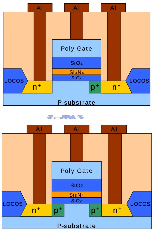
Figure 2-1(a) ~ 2-1(k) schematically depicts the process flow of the proposed SONOS flash memory with Zener junction. The fabrication process of the Zener junction SONOS flash memory devices involved was started with the LOCOS isolation process on p-type, 5-10 ohm-cm, (100) orientation, 150 mm silicon substrates. First, the tunneling oxide was thermally grown at 1000℃ with N2O and
O2 in vertical furnace system. The trapping layer Si3N4 was deposited at by low
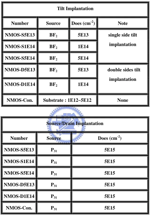
temperature chemical vapor deposition (LPCVD) at 780℃, 350mTorr. Then, we do a re-oxidation process step to slightly oxidize the surface of the nitride layer in order to improve the interface quality between the trapping layer and the blocking oxide (top oxide) layer. The locking oxide (top oxide) layer was deposited by LPCVD at 700℃, 300mTorr. Finally, the poly-gate was deposited by LPCVD at 660℃, 300mTorr. The thickness of poly-gate / oxide (blocking oxide) / nitride / oxide (tunneling oxide) are 200nm / 15nm / 8nm / 3nm respectively. Then, the gate was patterned by the exposure, development, and the etching step. Before the next implant steps, we deposited a oxide layer by LPCVD and then etch the oxide layer by dry etch process to from the sidewall spacer. The sidewall spacer is used to prevent the sidewall of the gate stack from being damaged during the implant process steps. For the n-channel SONOS memory devices, we first accomplished the reverse halo-implantation step using a tilt angle implantation with BF2 ion to
forming the p+ region. The dose and energy of the reverse halo implantation are shown in Table 2-1. The control devices is without the reverse halo implantation. Then, the source/drain n+ region was completed by P31 implant without tilt angle.
The dose and energy of the P31 implant are 5E15 cm-2 and 30 keV. Then, the
does 5E15 cm-2 and energy 40 keV. After these implantation process steps, the dopants were activated at 950℃ for 10 seconds by Rapid Thermal Anneal (RTA) system. Then, the 400nm passivation oxide was deposited by LPCVD. The contact holes were patterned and the Al metal deposition was done by PVD. Finally, we define the contact pad by metal etch.
P-substrate
LOCOS
LOCOS
Fig. 2-1 (a)
P-substrate
LOCOS
SiO2LOCOS
P-substrate
LOCOS
LOCOS
Si
3N
4 SiO2Fig. 2-1 (c)
P-substrate
LOCOS
LOCOS
SiO
2Si
3N
4 SiO2Poly Gate
P-substrate
LOCOS
LOCOS
SiO
2Si
3N
4 SiO2Fig. 2-1 (e)
Poly Gate
SiO
2Si
3N
4 SiO2P-substrate
LOCOS
LOCOS
Fig. 2-1 (f)
P-substrate
Poly Gate
SiO
2Si
3N
4 SiO2LOCOS
LOCOS
BF
2
F
ig. 2-1 (g)
P-substrate
p
+
p
+
Poly Gate
SiO
2Si
3N
4 SiO2LOCOS
LOCOS
BF
2
P-substrate
p
+
p
+
LOCOS
LOCOS
Poly Gate
SiO
2Si
3N
4 SiO2P
31
Fi
g. 2-1 (i)
P-substrate
p
+
p
+
LOCOS
LOCOS
Poly Gate
SiO
2Si
3N
4 SiO2P
31
Fig. 2-1 (j)
P-substrate
p
+
n
+
n
+
LOCOS
LOCOS
Poly Gate
SiO
2Si
3N
4 SiO2P-substrate
p
+
p
+
n
+
n
+
LOCOS
LOCOS
Poly Gate
SiO
2Si
3N
4 SiO2Fig. 2-1 (k)
P-substrate
p
+
n
+
n
+
LOCOS
LOCOS
Poly Gate
SiO
2Si
3N
4 SiO2Al
Al
Al
P-substrate
p
+
p
+
n
+
n
+
LOCOS
LOCOS
Poly Gate
SiO
2Si
3N
4 SiO2Al
Al
Al
Fig. 2-1 (l)
Tilt Implantation
Number Source
Does
(cm
-2)
Note
NMOS-S5E13 BF
25E13
NMOS-S1E14 BF
21E14
NMOS-S5E14 BF
25E14
single side tilt
implantation
NMOS-D5E13 BF
25E13
NMOS-D1E14 BF
21E14
double sides tilt
implantation
NMOS-Con.
Substrate : 1E12~5E12
None
Source/Drain Implantation
Number Source
Does
(cm
-2)
NMOS-S5E13 P
315E15
NMOS-S1E14 P
315E15
NMOS-S5E14 P
315E15
NMOS-D5E13 P
315E15
NMOS-D1E14 P
315E15
NMOS-Con. P
315E15
2.3 Result and Discussion
In this section, the electrical characteristics of n-channel SONOS flash memory were discussed.
2.3.1 Id-Vg Curve
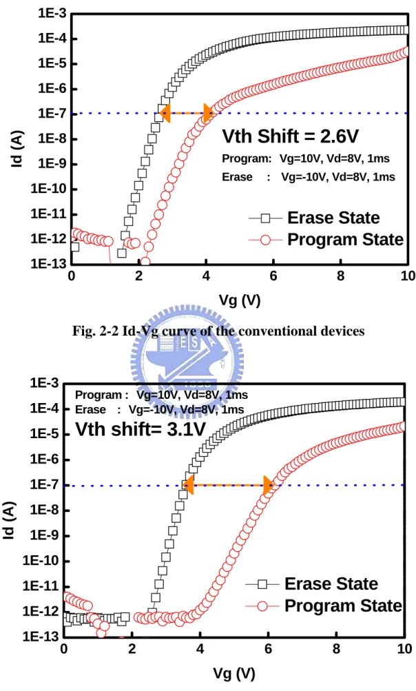
Figure 2-2 shows the Id-Vg curve of the conventional devices under programming and erasing operations and figure 2-3 shows the Zener devices. The constant current method was used to define the Vth (Id = 1nA). The program condition is Vg = 10V, Vd = 8V with 1ms stress. The erase condition is Vg = -10V, Vd = 8V with 1ms stress both in the conventional devices and in the Zener devices. The program condition is Vg = 10V, Vd = 8V with 1ms stress in both devices. The memory window in the conventional devices is about 2.6V, and it’s about 3.1V in the Zener devices. We use channel hot electron injection (CHE) as programming method and band to band hot hole (BBHH) as erasing method. Figure 2-4 shows the plot of CHE programming mechanism and figure 2-5 show the plot of BBHH erasing mechanism. We think the Vth Shift rightward is due to electron trapping in the trapping layer. Because that as we apply voltage on memory devices, the energy band will bend. And then electron trapping occurred. During program, the electrons in the substrate gain energy from applied Vg and Vd. If the energy is enough to overcome the energy barrier of tunneling oxide layer, the hot electrons will inject into the nitride trapping and be trapped. This phenomenon cause Vth shift. As erasing, a negative Vg and positive Vd were applied to generate hot holes in the substrate. If the hot hole gets enough energy to overcome the tunneling oxide energy barrier, it will arrive at trapping layer and then combine with electron in the nitride trapping layer. Then the Id-Vg curve shifts leftward.
0
2
4
6
8
10
1E-13
1E-12
1E-11
1E-10
1E-9
1E-8
1E-7
1E-6
1E-5
1E-4
1E-3
Erase State
Program State
Id
(A)
Vg (V)
Vth Shift = 2.6V
Program: Vg=10V, Vd=8V, 1ms Erase : Vg=-10V, Vd=8V, 1msFig. 2-2 Id-Vg curve of the conventional devices
0
2
4
6
8
10
1E-13
1E-12
1E-11
1E-10
1E-9
1E-8
1E-7
1E-6
1E-5
1E-4
1E-3
Erase State
Program State
Id
(A)
Vg (V)
Program : Vg=10V, Vd=8V, 1ms Erase : Vg=-10V, Vd=8V, 1msVth shift= 3.1V
n
+
Vg > 0
Vs = 0
Channel Hot Electron
Poly-Gate
SiO
2 SiNx SiO2Vd > 0
n
+
Hole
Electron
Vb = 0
Fig. 2-4 Channel hot electron injection (CHE) programming
mechanism
Vg < 0
Vs = 0
Band-to-Band Hot Hole
Poly-Gate
SiO
2 SiNx SiO2n
+
Vd> 0
n
+
Hole
Electron
Vb = 0
2.3.2 Program and Erase Speed
Figure 2-6 shows the programming speed of the single side Zener devices and the conventional devices. Fig. 2-7 shows the programming speed of the double side Zener devices and the conventional devices It show that the Zener devices is faster than the convention devices. The programming speed of Zener devices increases as the concentration of p+ region increasing. First, Figure 2-8 shows the tunneling oxide band diagram as programming state. First, because the electric field in p+/n+ junction is higher than in p/n+ junction, channel hot electron can get higher energy to overcome the tunneling oxide barrier. Second, when the p+ channel is in
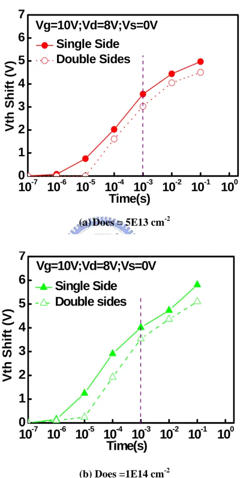
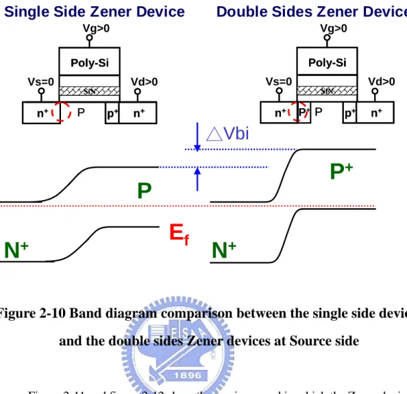
programming operation, the Zener devices will have more tunneling oxide bend banding than the conventional devices. Hence the electron injection efficiency in the Zener devices is higher than the conventional devices. From these two points, the programming speed can be improved with the Zener junction. And we can see the comparison between the single side Zener devices and the double sides Zener devices in figure 2-9. Because the double sides Zener has higher potential voltage (Vbi) at the source side junction as figure 2-10, it will decrease more electron energy of lateral direction.
10
-710
-610
-510
-410
-310
-210
-110
00
1
2
3
4
5
6
7
S5E14
S1E14
S5E13
Con.
Vg=10V;Vd=8V;Vs=0V
Vth Shift (V)
Time(s)
Single Side Zener Device
Fig. 2-6 Programming speed of the single side Zener devices and the
conventional devices
10
-710
-610
-510
-410
-310
-210
-110
00
1
2
3
4
5
6
7
D1E14
D5E13
Con.
Vg=10V;Vd=8V;Vs=0V
V
th Shift (V)
Time(s)
Double Sides Zener Device
Fig. 2-7 The programming speed of the double side Zener devices and
the conventional devices
Vg Ef
P
e -SiN e -n+ n+ Poly-Si Vg>0 Vs=0 Vd>0 n+ n+ Poly-SiP
SiN(a) The conventional devices
n
+n
+p
+Poly-Si
Vg>0
Vs=0
Vd>0
n
+n
+p
+Poly-Si
P
SiNVg
E
f SiNP
+e
-e
-e
-e
-(b) The Zener devices
10
-710
-610
-510
-410
-310
-210
-110
00
1
2
3
4
5
6
7
Vg=10V;Vd=8V;Vs=0V
Vt
h Sh
if
t (V)
Time(s)
Single Side
Double Sides
(a) Does = 5E13 cm
-210
-710
-610
-510
-410
-310
-210
-110
00
1
2
3
4
5
6
7
Vg=10V;Vd=8V;Vs=0V
V
th Shi
ft (V)
Time(s)
Single Side
Double sides
(b) Does =1E14 cm
-2Fig. 2-9 Programming speed comparison of the single side Zener
devices and the double sides Zener devices
n+ n+ p+ Poly-Si Vg>0 Vs=0 Vd>0 n+ n+ p+ Poly-Si P SiN P+ n+ n+ p+ Poly-Si Vg>0 Vs=0 Vd>0 n+ n+ p+ Poly-Si P SiN
Single Side Zener Device
Double Sides Zener Device
P
+
N
+
E
f
P
N
+
△Vbi
Figure 2-10 Band diagram comparison between the single side devices
and the double sides Zener devices at Source side
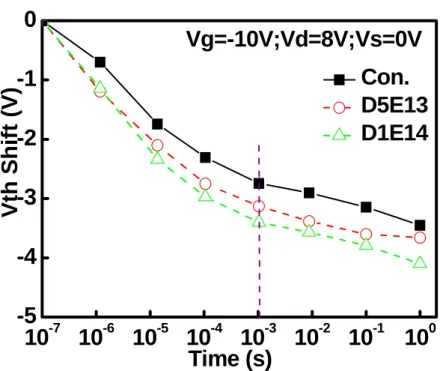
Figure 2-11 and figure 2-12 show the erasing speed in which the Zener devices is faster than the convention devices. The erasing speed of the Zener devices increased as the concentration of p+ region increasing. Figure 2-14 is the erasing state junction band diagram plot in our devices. When a positive voltage apply to gate node and negative bias to drain node, the n+/p+ junction were biased at reversed condition. The Zener devices shows the larger energy band bending, and it induces more hot holes direct band to band tunneling into the channel. So, the Zener devices have better erasing characteristics than the conventional devices. Figure 2-13 displays that in the same does condition the erasing speed of the single side Zener devices and the double sides Zener devices are similar.
10
-710
-610
-510
-410
-310
-210
-110
0-5
-4
-3
-2
-1
0
Vg=-10V;Vd=8V;Vs=0V
Vth Shif
t (V)
Time (s)
Con.
S5E13
S1E14
S5E14
Figure 2-11 Erasing speed of the single side Zener devices and the
convention devices
10
-710
-610
-510
-410
-310
-210
-110
0-5
-4
-3
-2
-1
0
Con.
D5E13
D1E14
Time (s)
V
th S
h
ift (V
)
Vg=-10V;Vd=8V;Vs=0V
Figure 2-12 Erasing speed of the double sides Zener devices and the
convention devices
10
-710
-610
-510
-410
-310
-210
-110
0-5
-4
-3
-2
-1
0
Time (s)
Vth Shift (V)
Single Side
Double Side
Vg= - 10 V
Vd= 8 V
Vs= 0 V
(a) Does = 5E13 cm
-210
-710
-610
-510
-410
-310
-210
-110
0-5
-4
-3
-2
-1
0
Time (s)
V
th Shift (V)
Vg= - 10 V
Vd= 8 V
Vs= 0 V
Single Side
Double Side
(b) Does = 1E14 cm
-2Fig. 2-13 Erasing speed of the single side Zener devices and the double
sides Zener devices
P
N
+E
fE
f h+ h+n
+n
+Poly-Si
Vg<0
Vs=0
Vd>0
n
+n
+Poly-Si
P
SiN(a) The conventional devices
P
+N
+E
fE
f h+ h+ h+ h+n
+n
+p
+Poly-Si
Vg<0
Vs=0
Vd>0
n
+n
+p
+Poly-Si
P
SiN(b) The Zener devices
2.3.3 Data Retention Characteristic
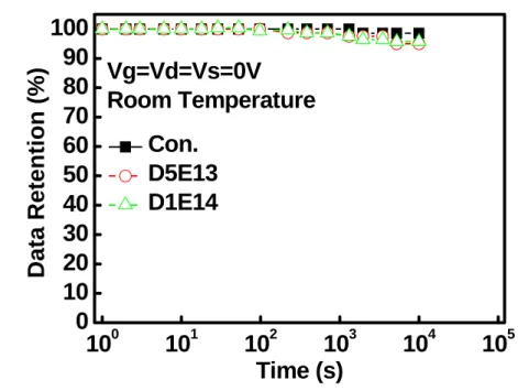
Figure 2-15 is the data retention characteristic of the single side Zener devices and the conventional devices measured at room temperature, and figure 2-16 is
retention compared between the double sides Zener devices and the conventional devices. We find the charge loss after 1E4 seconds of the double sides Zener
junction memory devices shows little difference with the conventional devices. But the single side Zener junction memory devices has much more charge loss
comparing to the conventional devices as the does of halo implantation increasing. The curve shows 10% ~ 20% charge loss as measure time up to 1E4 seconds at room temperature. Because the larger lateral electrical field in the single side Zener devices, it caused the gate control ability lowing. And the partial charge stored in the trapping layer and the tunneling oxide interface and in the tunneling oxide layer, as figure 2-17, the charge in this region loss easily. But the most of the stored charge is in the trapping layer in the double sides devices, because of the better gate control ability, as figure 2-18. Hence, the double sides Zener devices have better data retention compared with the single side Zener devices.
10
010
110
210
310
410
50
10
20
30
40
50
60
70
80
90
100
Time (s)
Dat
a
Ret
e
n
tion
(%
)
Vg=Vd=Vs=0V
Room Temperature
Con.
S5E13
S1E14
S5E14
Fig. 2-15 Data retention characteristic of the single side Zener devices
and the conventional devices
10
010
110
210
310
410
50
10
20
30
40
50
60
70
80
90
100
Vg=Vd=Vs=0V
Room Temperature
Data Re
tention (%)
Time (s)
Con.
D5E13
D1E14
Fig. 2-16 is retention compared between the double sides Zener devices
and the conventional devices.
Vg > 0
Vs = 0
Poly-Gate
SiO
2 SiNx SiO2Vd > 0
n+
p+
Electron
Vb = 0
Fig. 2-17 Charge stored location in the single side Zener devices
Vg > 0
Vs = 0
Poly-Gate
SiO
2 SiNx SiO2Vd > 0
n+
p+
Electron
Vb = 0
2.3.4 Drain Disturbance Measurement
When we operate the memory devices at either programming state or erasing state, we always apply a positive drain voltage to the bit line. Hence, the drain voltage does not only be applied to the cell we want to operate but also to the other devices cell, figure 2-19. And then the voltage maybe enhances the charge loss in the trapping layer, and this is called drain disturbance. Figure 2-20, 2-21, 2-22, and 2-23 show drain disturbance measurement of the Zener devices and the
conventional devices. We applied two drain bias conditions, Vd = 8V and 10V with Vg = Vs = Vb = 0V to the all devices. From figure 2-21 and 2-23, we find that the drain disturbance is more serious in the single side Zener devices than the
conventional devices. But it is still acceptable to the double sides Zener devices. The reason is that the p+/n+ junction has higher electric field with positive Vd applied than the p/n+ junction. And the charge stored location in the single side Zener devices is in the tunneling oxide or the interface of the trapping layer and the tunneling oxide layer, the charge losses in the region more easily than in the
trapping layer. Vd>0 e -e -Selected cell Unselected cells ( Programming state ) Selected WL
10
010
110
210
3-3.0
-2.5
-2.0
-1.5
-1.0
-0.5
0.0
Con.
S5E13
S1E14
S5E14
Vd=8V;Vg=Vs=0V
Vth Shi
ft (V)
Time(s)
Fig. 2-20 Drain disturbance between the single side Zener devices and
the conventional devices at Vd = 8V
10
010
110
210
3-3.0
-2.5
-2.0
-1.5
-1.0
-0.5
0.0
Time (s)
Vth Shift (V)
Vd=8V;Vg=Vs=0V
Con.
D5E13
D1E14
Fig. 2-21 Drain disturbance between the double sides Zener devices
and the conventional devices at Vd = 8V
10
010
110
210
3-3.0
-2.5
-2.0
-1.5
-1.0
-0.5
0.0
Vd=10V;Vg=Vs=0V
Vth Shift (V)
Time (s)
Con.
S5E13
S1E14
S5E14
Fig. 2-22 Drain disturbance between the single side Zener devices and
the conventional devices at Vd = 10V
10
010
110
210
3-3.0
-2.5
-2.0
-1.5
-1.0
-0.5
0.0
Time (s)
Vth Shi
ft (V)
Vd=10V;Vg=Vs=0V
Con.
D5E13
D1E14
Fig. 2-23 Drain disturbance between the double sides Zener devices
and the conventional devices at Vd = 10V
2.3.5 Endurance Characteristic
Figure 2-24, 2-25, and 2-26 display the endurance characteristic of the
conventional devices, the single side Zener devices, and the double sides Zener devices. We find that the endurance in the conventional is the worst case and the Zener shows the better endurance characteristic. First, because the higher operation speed can reduce the stress time and reduce the nitride quality degradation. Second, due to the difference between the programming and erasing mechanism, the
locations of charge stored are not wholly the same. Then the stored electron by CHE programming mechanism can not be combined with hole injection by BBHH erasing mechanism. In the Znener devices, the locations of charge injection
between programming and erasing are more closely, due to the higher electric field region could make the charge more convergent.
10
010
110
210
310
410
52
3
4
5
6
7
8
9
10
Vt
h
(V)
The Number of P/E Cycle
Con.
10
010
110
210
310
410
52
3
4
5
6
7
8
9
10
Vt
h
(
V)
The Number of P/E Cycle
S5E13
Fig. 2-25 Endurance characteristic of the single side Zener devices
10
010
110
210
310
410
52
3
4
5
6
7
8
9
10
Vt
h
(
V)
The Number of P/E Cycle
D5E13
2.4 Summary
The impacts of tilt implantation on programming and erasing performance are beneficial for the SONOS devices. We can make injection efficiency higher during CHE programming and BBHH erasing to get better programming and erasing speed with the higher electrical field. Although the Zener devices shows
degradation in the data retention and drain disturbance, but it is still acceptable in the SONOS memory. Because we decrease the programming and erasing stress time at the same bias condition, the endurance characteristics in both single side Zener devices and double sides Zener devices are better than the conventional devices. So we think that the Zener devices surely could improve the SONOS memory characteristics.
2-5 Reference
[1].Ielmini, D.; Spinelli, A.S.; Lacaita, A.L.; Leone, R.; Visconti, A.; “Localization of SILC in flash memories after program/erase cycling”Reliability Physics Symposium
Proceedings, 2002. 40th Annual 7-11 April 2002 Page(s):1 – 6
[2].Chung, S.S.; Yih, C.M.; Ho, Z.H.; Lin, C.J.; Kuo, D.S.; Liang, M.S.;” The dominant mechanisms of hot-hole injection induced SILC and their correlation with disturbs in N-flash memory cells”VLSI Technology, Systems, and Applications, 1999. International
Symposium on 8-10 June 1999 Page(s):258 – 261
[3]. Cherng-Ming Yih; Zhi-Hao Ho; Mong-Song Liang; Chung, S.S.”Characterization of hot-hole injection induced SILC and related disturbs in flash memories” Electron
Devices, IEEE Transactions on Volume 48, Issue 2, Feb. 2001 Page(s):300 – 306
[4].B.D. Salvo, C. Gerardi, R. V. Schaijk, S.A. Lombardo, D. Corso, C. Plantamura, T. Serafion, G. Ammendola, M. V. Duuren, P. Goarin, W. Y. Mei, K. V. D. Jeugd, H. Baron, M. Gely, P. Mur, and S. Deleonibus, IEEE Trans. Device and Materials Reliability, 4,
377(2004).
[5].M. L. French, CY Chen, H Sathianathan, MH White, “Design and scaling of a SONOS multidielectric device for nonvolatile memory applications” IEEE Trans.
Compon., Packag. Manuf. Technol., 1994.
[6].Sangmoo Choi, Myungjun Cho, Jung Woo Kim and Hyunsang Hwang, “Improved metal–oxide–nitride–oxide–silicon-type flash device with high-k dielectrics for blocking layer” JOURNAL OF APPLIED PHYSICS, vol. 94, pp. 5409-5410, 2003.
[7].J. Bu and M. H. White, “Design considerations in scaled SONOS nonvolatile memory devices” Solid-State Electron. 2001.
[8].F. R. Libsch, MH White, “Charge transport and storage of low programming voltage SONOS/MONOS memory devices.” Solid-State Electron. 1990.
CHAPTER 3
Characteristics of P-Channel SONOS Memory
with Zener Junction
3.1 Introduction
Due to its low voltage, low power and high speed programming features, p-channel flash memories [1]-[2] have been evolved as a promising cell for real applications in the future. In a certain design of p-channel flash cells, programming of the cell can be achieved either by band-to-band tunneling induced hot electron injection (BBHHIHE)at the drain side or by channel hot hole impact ionization induced channel hot electron injection (CHHIHE). Erasing of the cell can be accomplished by electron channel Fowler-Nordheim(F-N) ejection from the floating gate. Here, both Programming schemes, CHHIHE and BBHHIHE, will generate the so-call oxide damages, which include the interface state and the oxide trap charge [3]. The interface traps density generated under these kinds of Fowler-Nordheim (F-N) stress and Substrate-hot-hole stress. The injection of impact ionization generated hot holes is found to be the most important reason for interface trap generation under VG<0 F-N
stress at high oxide field. The generated interface-trap density under Substrate hot hole stress increases with increasing gate oxide field. It is also found that the Substrate hot hole stress induces more interface traps than Substrate hot electron stress.
Instead of using N-channel cells, P-channel cells[5]-[13], known for the high injection efficiency and low programming drain current, are quite suitable for low-voltage and low-power applications. The developing trend of Flash memory has gone in the way of multi-level storages. The most important issue is to precisely control a tight threshold voltage distribution at different levels. To achieve tight threshold
voltage distribution in multi-level Flash memory, the bit-by-bit verification which slows down the programming speed can be performed. The multi-level applications of P-channel Flash memory was first proposed in [14-19].
In this work, we purpose a high operation speed SONOS memory with using reverse halo implant in the channel near by Source / Drain sides to improve the programming / erasing speed. Figure 3-1, 3-2 and 3-3 display the programming mechanism and the erasing mechanism of p-channel SONOS memory respectively. Because the erasing mechanism in the p-channel memory is F-N tunneling, the erasing speed is not fast enough. We make a little change in the erasing mechanism here. Because the charge stored locations by CHHIHE and BBHHIHE are near the drain edge, we focus on this region. Hence we use drain side FN tunneling to be our erasing mechanism, and this way also can be improved by higher field. Then the problem of the injection efficiency during erasing is improved in the p-channel SONOS memory. Due to the CHHIHE mechanism is slower than BBHHIHE mechanism; we use the BBHHIHE as programming mechanism in our study. Because of the injection locations between BBHHIHE and drain side FN tunneling in p-channel memory are more closely than n-channel memory, we expect that the endurance will be improved.
p
+
Band-to-Band Hot Hole Induced Hot Electron
Poly-Gate
SiO
2 SiNx SiO2p
+
Vg > 0
Vs = 0
Vd < 0
Hole
Electron
Vb = 0
Fig 3-1 Band to band hot hole induced hot electron programming
mechanism
p
+
Vg < 0
Vs = 0
Channel Hot Hole Induced Hot Electron
Poly-Gate
SiO
2 SiNx SiO2Vd < 0
p
+
Hole
Electron
Vb = 0
Fig 3-2 Channel hot hole induced hot electron programming
p
+
Vg < 0
Floating
Drain Side F-N Erase
Poly-Gate
SiO
2 SiNx SiO2V
D> 0
p
+
Hole
Electron
Vb = 0
3.2 Experiment
Figure 3-4 schematically depicts the process flow of the proposed SONOS flash memory with Zener junction. The fabrication process of the Zener junction SONOS flash memory devices involved was started with the LOCOS isolation process on p-type, 5-10ohm-cm, (100) orientation, 150mm silicon substrates. First, the tunneling oxide was thermally grown at 1000℃ with N2O and O2 in vertical
furnace system. The trapping layer Si3N4 was deposited at by low temperature
chemical vapor deposition (LPCVD) at 780 ℃ , 350mTorr. Then, we do a re-oxidation process step to slightly oxidize the surface of the nitride layer in order to improve the interface quality between the trapping layer and the blocking oxide (top oxide) layer. The locking oxide (top oxide) layer was deposited by LPCVD at 700℃, 300mTorr. Finally, the poly-gate was deposited by LPCVD at 660℃, 300mTorr. The thickness of poly-gate / oxide (blocking oxide ) / nitride / oxide (tunneling oxide) are 200nm / 15nm / 8nm / 3nm respectively. Then, the gate was patterned by the exposure, development, and the etching step. Before the next implant steps, we deposited a oxide layer by LPCVD and then etch the oxide layer by dry etch process to from the sidewall spacer. The sidewall spacer is used to prevent the sidewall of the gate stack from being damaged during the implant process steps. For the n-channel SONOS memory devices, we first accomplished the reverse halo-implantation step using a tilt angle implantation with P31 ion to
forming the n+ region. The dose and energy of the tilt implantation are shown in Table 3-1. The control device is without the reverse halo implantation. Then, the source/drain p+ region was completed by BF2 implant without tilt angle. The dose
and energy of the BF2 implant are 5E15cm-2 and 50keV. Then, the substrate contact
energy 40keV. After these implantation process steps, the dopants were activated at 950℃ for 10 seconds by Rapid Thermal Anneal (RTA) system. Then, the 400nm passivation oxide was deposited by LPCVD. The contact holes were patterned and the Al metal deposition was done by PVD. Finally, we define the contact pad by metal etch.
N-substrate
LOCOS
LOCOS
Fig. 3-4 (a)
N-substrate
N-substrate
LOCOS
LOCOS
Si
3N
4 SiO2Fig. 3-4 (c)
N-substrate
LOCOS
LOCOS
SiO
2Si
3N
4 SiO2Fig. 3-4 (d)
Poly Gate
N-substrate
LOCOS
LOCOS
SiO
2Si
3N
4 SiO2Fig. 3-4 (e)
Poly Gate
SiO
2Si
3N
4 SiO2N-substrate
LOCOS
LOCOS
N-substrate
P
31
Poly Gate
SiO
2Si
3N
4 SiO2LOCOS
LOCOS
Fig. 3-4 (g)
BF
2
N-substrate
n
+
n
+
LOCOS
LOCOS
Poly Gate
SiO
2Si
3N
4 SiO2Fig. 3-4 (h)
P-substrate
n
+
p
+
p
+
LOCOS
LOCOS
Poly Gate
SiO2
Si
3N
4 SiO2Fig. 3-4 (i)
N-substrate
n
+p
+p
+ LOCOS LOCOSPoly Gate
SiO2 Si3N4 SiO2Al
Al
Al
Fig. 3-4 (j)
Tilt Implantation
Number Source
Does
(cm
-2)
Note
PMOS-5E13 P
315E13
PMOS-1E142 P
311E14
PMOS-5E14 P
315E14
Single side tilt
implantation
PMOS-Con. Substrate:1E12~5E12
Source/Drain Implantation
Number Source
Does
(cm
-2)
PMOS-S5E13 BF2
5E15
PMOS-S1E14
BF2
5E15
PMOS-S5E14
BF2
5E15
PMOS-Con.
BF2
5E15
3.3 Results and Discussion
In this section, the electrical characteristics of n-channel SONOS flash memory were discussed.
3.3.1 Id-Vg Curve
Figure 3-4 shows the Id-Vg curve of the conventional device under programming and erasing operations and figure 3-5 shows the Zener device ones. We use the constant current method to define the Vth (Id = 1 nA) here. We employ band-to-band
tunneling induced hot electron injection (BBHHIHE) method to program the device and drain side FN method to erase device. And, because of the programming speed by the CHHIHE method is not efficiency, we employ the BBHHIHE method as our programming operation. The programming condition is Vg = 10V, Vd = -8V with 50 ms stress. The erasing condition is Vg = -10V, Vd = 8V with 10 ms stress and the source node is floating. Figure 3-1 shows the programming mechanism plot and figure 3-3 shows the erasing mechanism plot. The Vth of the conventional device between
programming state and erasing state is about 2.7V shift. And the Vth of the Zener device between programming state and erasing state is about 3.8V shift. We think the Vth Shift rightward is due to electron injection into the trapping layer. When we give a voltage to memory device, the energy band bending will occur. And then carriers injection
occurred during programming and erasing operation. Under programming operation, the electrons in the substrate gain energy from applied Vg and Vd. If the energy is enough to overcome the energy barrier, the hot electrons will inject into the nitride trapping and then be trapped. The phenomenon caused Vth shift. As erasing, the positive Vd would make the p+/n+ junction at forward state, and generate more electron-hole pairs in the substrate. Then the negative Vd would supply holes energy to injecte into the trapping layer, and then Id-Vg curve shifts leftward.
-14
-12
-10
-8
-6
-4
10
-1310
-1210
-1110
-1010
-910
-810
-710
-610
-510
-4Id (A)
Vg (V)
Erase StateProgram State (by BBHHIHE) Program State (by CHHIHE)
Program:Vg=10V, Vd=-8V, tp=50ms
Erase:Vg=-10V, Vd=8V, te=10ms
△Vth = 2.7V
△Vth = 0.7V
Fig. 3-5 Id-Vg curve of the conventional device
-14
-12
-10
-8
-6
-4
10
-1310
-1210
-1110
-1010
-910
-810
-710
-610
-510
-4 Erase StateProgram State (by BBHHIHE) Program State (by CHHIHE)

![HPSH [ 氧化數平衡反應式係數 ]](data:image/gif;base64,R0lGODlhAQABAIAAAP///wAAACH5BAEAAAAALAAAAAABAAEAAAICRAEAOw==)