IEEE ELECTRON DEVICE LETTERS, VOL. 33, NO. 12, DECEMBER 2012 1693
Origin of Hopping Conduction in Sn-Doped Silicon
Oxide RRAM With Supercritical
CO
2
Fluid Treatment
Tsung-Ming Tsai, Kuan-Chang Chang, Ting-Chang Chang, Geng-Wei Chang, Yong-En Syu, Yu-Ting Su,
Guan-Ru Liu, Kuo-Hsiao Liao, Min-Chen Chen, Hui-Chun Huang, Ya-Hsiang Tai,
Der-Shin Gan, Cong Ye, Hao Wang, and Simon M. Sze
Abstract—In this letter, we investigate the origin of hopping
conduction in the low-resistance state (LRS) of a resistive random access memory device with supercritical CO2fluid treatment. The dangling bonds of a tin-doped silicon oxide (Sn:SiOx) thin film
were cross linked by the hydration–dehydration reaction through supercritical fluid technology. The current conduction mechanism of the LRS in the posttreated Sn:SiOxthin film was transferred
to hopping conduction from Ohmic conduction, owing to isolation of metal tin in the Sn:SiOx thin film by hydration–dehydration
reaction. The phenomena can be verified by our proposed re-action model, which is speculated by the X-ray photoelectron spectroscopy analyses.
Index Terms—Hopping conduction, hydration–dehydration
re-action, resistance random access memory (RRAM), supercritical fluid.
I. INTRODUCTION
T
O SURMOUNT the technical and physical limitation issues of conventional charge storage-based memory de-vices [1]–[5], the resistance random access memory (RRAM) device is constructed of an insulating layer sandwiched by two electrodes. This is a great potential candidate for the next-generation nonvolatile memory due to their superior char-acteristics such as lesser cost, simple structure, high-speed operation, and nondestructive readout [6], [7].Manuscript received June 26, 2012; revised August 19, 2012; accepted September 1, 2012. Date of publication October 22, 2012; date of current version November 22, 2012. This work was supported by the National Science Council of the Republic of China under Contract NSC-100-2120-M-110-003 and Contract NSC 100-2221-E-110-060. The review of this letter was arranged by Editor M. Jurczak.
T.-M. Tsai, K.-C. Chang, K.-H. Liao, H.-C. Huang, and D.-S. Gan are with the Department of Materials and Optoelectronic Science, National Sun Yat-Sen University, Kaohsiung 804, Taiwan.
T.-C. Chang, Y.-E. Syu, Y.-T. Su, G.-R. Liu, and M.-C. Chen are with the Department of Physics, National Sun Yat-Sen University, Kaohsiung 804, Taiwan, and also with the Advanced Optoelectronics Technology Center, National Cheng Kung University, Tainan 701, Taiwan (e-mail: tcchang@ mail.phys.nsysu.edu.tw).
G.-W. Chang and Y.-H. Tai are with the Department of Photonics and the Institute of Electro-Optical Engineering, National Chiao Tung University, Hsinchu 300, Taiwan.
C. Ye and H. Wang are with the Faculty of Physics and Electronic Technol-ogy, Hubei University, Wuhan 430062, China.
S. M. Sze is with the Department of Physics, National Sun Yat-Sen Uni-versity, Kaohsiung 804, Taiwan and also with the Department of Electronics Engineering, National Chiao Tung University, Hsinchu 300, Taiwan.
Color versions of one or more of the figures in this letter are available online at http://ieeexplore.ieee.org.
Digital Object Identifier 10.1109/LED.2012.2217932
In our previous research, supercritical CO2 (SCCO2) fluid
technology was used to improve the dielectric properties and performance of various thin-film transistors (TFTs), e.g., hydrogenated amorphous-silicon TFTs and ZnO TFTs [8]–[15]. Supercritical phase is peculiar with its characteristics of high penetration of gas and solubility of liquid. The property of supercritical water fluid has tremendous oxidation [16]. However, high critical temperature and high critical pressure are essential condition to lead to supercritical water fluid, which is difficult to achieve through modern facilities. By adding a little water into supercritical CO2 fluids, the liquid
water can achieve the phase of supercritical fluids due to the phase close to the idea solution.
The material of Sn-doped silicon oxide (Sn:SiOx) used as
a resistive switching layer has been studied in our previous work [17]. Therefore, the Pt/Sn : SiOx/TiN sandwiched
de-vices were fabricated to investigate the effect of SCCO2 on
resistive switching properties of Sn:SiOx thin films. The
ef-fects of SCCO2 treatment on resistive switching behaviors of
Sn:SiOxthin films were evaluated by material and carrier
con-duction mechanism analyses. Because the supercritical fluid has gaslike and high-pressure properties to effectively diffuse into nanoscale without damage [18], the dangling bonds of Sn:SiOx
thin films were cross linked by the hydration–dehydration reaction.
II. EXPERIMENTALSETUP
The experimental specimens were prepared as follows: the Sn:SiOx thin film (about 30 nm) was deposited on the
TiN/Ti/SiO2/Si substrate by cosputtering with the pure SiO2
and Sn targets. The sputtering power was fixed at RF power of 200 and 3 W for SiO2 and Sn targets, respectively. The
cosputtering was executed in argon ambient (Ar = 30 sccm) with a working pressure of 6 mTorr at room temperature. In contrast, the Sn:SiOxthin films were put into the supercritical
fluid system with 165-mL chamber size, and then, the SCCO2
fluid mixed with 0.5-mL water were syringed into the reactive chamber to treat the specimens. Therefore, the water will be solved into SCCO2 fluids with a mole concentration of
0.17 M in the reactive chamber. During the treatment, the water-mixed supercritical CO2 fluids were heated and pressured to
120 ◦C and 3000 lbf/in2, respectively, in the stainless steel chamber of the supercritical fluid system for 1 h. Ultimately, the Pt top electrode with a thickness of 200 nm was de-posited on the Sn:SiOxthin film to form electrical devices with 0741-3106/$31.00 © 2012 IEEE
1694 IEEE ELECTRON DEVICE LETTERS, VOL. 33, NO. 12, DECEMBER 2012
Fig. 1. (a) Forming current curves of the Sn:SiOxRRAM devices before and after SCCO2 treatment. (b) Black and red curves are the resistive switching
characteristics of the Sn:SiOxfilm before and after SCCO2treatment,
respec-tively. The current of the posttreated Sn:SiOxfilm is reduced.
Pt/Sn : SiOx/TiN sandwich structures by dc magnetron
sput-tering. The entire electrical measurements of devices with the Pt electrode of 250-μm diameter were performed using Agilent B1500 semiconductor parameter analyzer. In addition, X-ray photoelectron spectroscopy (XPS) was used to analyze the chemical composition and bonding of these insulator materials, respectively.
III. RESULTS ANDDISCUSSION
The “forming process” is required to activate all of the Sn:SiOx RRAM devices, using dc voltage sweeping with a
compliance current of 2 mA. The forming current of the Sn:SiOx RRAM devices after SCCO2 treatment was lower
than that of pretreatment devices [see Fig. 1(a)]. After the forming process, the electrical current–voltage properties of the Sn:SiOxdevices were compared before and after SCCO2
treat-ment [Fig. 1(b)]. The current of Sn:SiOxdevices is reduced at
0.1-V reading voltage after SCCO2treatment.
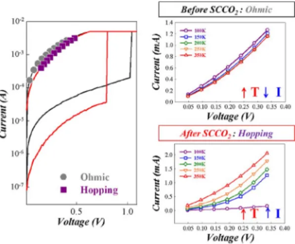
To investigate the interesting phenomena, we analyzed the current conduction mechanism of the Sn:SiOx thin film with
and without SCCO2 treatment, as shown in Fig. 2. The
cur-rent conduction in the high resistance state of the Sn:SiOx
device was transferred to the Schottky emission from the Poole–Frenkel conduction after SCCO2 treatment. These
phe-nomena were attributed to the improvement of dielectric prop-erties using SCCO2 treatment, which have been reported in
our previous study [9]. On the other hand, the carrier trans-port in the low-resistance state (LRS) of the Sn:SiOx device
was dominated by ohmic conduction in the Sn:SiOx layer.
According to the relationship of hopping conduction, J =
Fig. 2. Current conduction curves in the Sn:SiOx film before and after SCCO2treatment. The fitting of current curves for the Sn:SiOxfilm with and without SCCO2treatment was dominated by hopping conduction and Ohmic
conduction mechanisms, respectively.
Fig. 3. XPS spectra of Sn 3d5/2and Si 2p core levels in the Sn:SiOxfilm before and after SCCO2treatment. The mole fraction of metallic tin and Si–OH
bonds in the Sn:SiOxfilm are reduced obviously, but that of tin oxide and silicon oxide bonds are increased after SCCO2treatment.
qN aυ0e−qφT/kTeqaV /2dkT, where N , a, φT, υ0, and d are
the density of space charge, the mean of hopping distance, the intrinsic vibration frequency, the barrier height of hopping, and the film thickness, respectively; the current conduction mecha-nism will transfer to hopping conduction because of the change of material properties after SCCO2 treatment. Therefore, we
utilized the material spectra analyses to find out the reason of the electrical transfer mechanism from ohmic conduction to hopping conduction.
Compared with the peak area of Sn, Si, and O XPS spec-tra, the mole fraction of Sn:Si:O in the cosputtered Sn:SiOx
film was 0.3%:29.5%:70.2%. According to the XPS spectra analyses for the Sn 3d5/2 core level (see Fig. 3), the mole
fraction of Sn–O bond was greatly raised, but that of the Sn element was decreased in the Sn:SiOx thin film after SCCO2
treatment. In addition, the mole fraction of the Si–O bond was substantially increased in contrast with that of the Si–OH bond after SCCO2treatment in terms of the XPS spectra analyses of
the Si 2p core level. Therefore, the degree of oxidation would be increased, which is accompanied with dehydration in the SCCO2-posttreated Sn:SiOxthin film.
TSAI et al.: ORIGIN OF HOPPING CONDUCTION IN Sn-DOPED SILICON OXIDE RRAM 1695
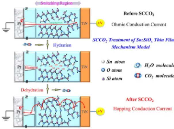
Fig. 4. Schematic of the carrier hopping effect in Sn:SiOx RRAM due to hydration–dehydration reaction mechanism through SCCO2treatment.
Based on the electrical and material analyses, we proposed a reaction model to explain the transfer of carrier conduction mechanism of the Sn:SiOx film with SCCO2 treatment, as
shown in Fig. 4. The conductive filament will be formed in the pretreatment Sn:SiOx film after the forming process. The
conductive filament will be connected with a dangling bond in the switching region of the film. The carriers were trans-ported through these dangling bonds, leading to the current conduction dominated by ohmic conduction. If the Sn:SiOx
film was put into the SCCO2 fluid environment, the H2O
molecule was carried into the grain boundary of the film by SCCO2fluid, which is attributed to the high penetration ability
of SCCO2fluid. The H2O molecule was approached to grain
boundary leading to the hydration reaction in the Sn:SiOxfilm.
Then, monomolecular CO2 in supercritical fluids induces the
dehydration of neighbor hydroxyl groups to form Si–O–Si and Sn–O–Si cross-linking bonding in the film. Hence, the tin metal in the Sn:SiOxthin film will be isolated by SCCO2treatment.
Only if the conductive filament formed in the Sn:SiOxfilm, the
carrier will hop through the isolated tin metal in the switching region of the posttreated film. This phenomena will make the electrical current conduction in the LRS of the Sn:SiOxfilm to
transfer from Ohmic conduction to hopping conduction. IV. CONCLUSION
In conclusion, the current conduction mechanism of the LRS in the Sn-doped silicon oxide RRAM device is transferred to hopping conduction by supercritical fluid treatment. The water molecule can be brought into the film to crossly link the dangling bond of the grain boundary in the resistive switching layer by supercritical CO2fluid. In virtue of the phenomena, the
tin metal of Sn:SiOxwill be isolated by hydration–dehydration
reaction of SCCO2 fluids. Only if the conductive filament
formed in the Sn:SiOxfilm, the electrical carriers of the RRAM
devices with SCCO2fluid treatment will be transported through
the isolated tin metal by hopping effect. ACKNOWLEDGMENT
The authors would like to thank the National Science Council Core Facilities Laboratory for Nano-Science and Nano-Technology in the Kaohsiung–Pingtung area where the experiment in this paper was performed.
REFERENCES
[1] T. C. Chang, F. Y. Jian, S. C. Chen, and Y. T. Tsai, “Developments in nanocrystal memory,” Mater. Today, vol. 14, no. 12, pp. 608–615, Dec. 2011.
[2] D. Jiang, M. Zhang, Z. Huo, Q. Wang, J. Liu, Z. Yu, X. Yang, Y. Wang, B. Zhang, J. Chen, and M. Liu, “A study of cycling induced degradation mechanisms in Si nanocrystal memory devices,” Nanotechnology, vol. 22, no. 25, p. 254009, Jun. 2011.
[3] F. M. Yang, T. C. Chang, P. T. Liu, P. H. Yeh, Y. C. Yu, J. Y. Lin, S. M. Sze, and J. C. Lou, “Memory characteristics of Co nanocrystal memory device with HfO2as blocking oxide,” Appl. Phys. Lett., vol. 90,
no. 13, pp. 132102-1–132102-3, Mar. 2007.
[4] J. Liu, Q. Wang, S. Long, M. Zhang, and M. Liu, “ Metal/Al2O3/ZrO2/
SiO2/Si (MAZOS) structure for high-performance non-volatile
mem-ory application,” Semicond. Sci. Technol., vol. 25, no. 5, p. 055013, May 2010.
[5] F. M. Yang, T. C. Chang, P. T. Liu, U. S. Chen, P. H. Yeh, Y. C. Yu, J. Y. Lin, S. M. Sze, and J. C. Lou, “Nickel nanocrystals with HfO2
blocking oxide for nonvolatile memory application,” Appl. Phys. Lett., vol. 90, no. 22, pp. 222104-1–222104-3, May 2007.
[6] Y. Wang, Q. Liu, S. Long, W. Wang, Q. Wang, M. Zhang, S. Zhang, Y. Li, Q. Zuo, J. Yang, and M. Liu, “Investigation of resistive switching in Cu-doped HfO2thin film for multilevel non-volatile memory applications,”
Nanotechnology, vol. 21, no. 4, p. 045202, Jan. 2010.
[7] Y. E. Syu, T. C. Chang, T. M. Tsai, Y. C. Hung, K. C. Chang, M. J. Tsai, M. J. Kao, and S. M. Sze, “Redox reaction switching mech-anism in RRAM device with Pt/CoSiOX/TiN structure,” IEEE Electron Device Lett., vol. 32, no. 4, pp. 545–547, Apr. 2011.
[8] C. T. Tsai, T. C. Chang, P. T. Liu, P. Y. Yang, Y. C. Kuo, K. T. Kin, P. L. Chang, and F. S. Huang, “Low-temperature method for enhancing sputter-deposited HfO2 films with complete oxidization,” Appl. Phys.
Lett., vol. 91, no. 1, pp. 012109-1–012109-3, Jul. 2007.
[9] C. T. Tsai, T. C. Chang, K. T. Kin, P. T. Liu, P. Y. Yang, C. F. Weng, and F. S. Huang, “A low temperature fabrication of HfO2films with
supercrit-ical CO2fluid treatment,” J. Appl. Phys., vol. 103, no. 7, pp. 074108-1–
074108-6, Apr. 2008.
[10] M. C. Chen, T. C. Chang, S. Y. Huang, K. C. Chang, H. W. Li, S. C. Chen, J. Lu, and Y. Shi, “A low-temperature method for improv-ing the performance of sputter-deposited ZnO thin-film-transistors with supercritical fluid,” Appl. Phys. Lett., vol. 94, no. 16, pp. 162111-1– 162111-3, Apr. 2009.
[11] C. T. Tsai, P. T. Liu, T. C. Chang, C. W. Wang, P. Y. Yang, and F. S. Yeh, “Low-temperature passivation of amorphous-silicon thin-film transistors with supercritical fluids,” IEEE Electron Device Lett., vol. 28, no. 7, pp. 584–586, Jul. 2007.
[12] C. T. Tsai, T. C. Chang, P. T. Liu, Y. L. Cheng, K. T. Kin, and F. S. Huang, “Application of supercritical CO2 fluid for dielectric
im-provement of SiOx film,” Electrochem. Solid State Lett., vol. 12, pp. H35– H37, 2009.
[13] M. C. Chen, T. C. Chang, S. Y. Huang, K. C. Chang, H. C. Huang, S. C. Chen, J. Liu, D. S. Gan, N. J. Ho, T. F. Young, G. W. Jhang, and Y. H. Tai, “Improvement of the performance of ZnO TFTs by low-temperature supercritical fluid technology treatment,” Surf. Coat.
Tech-nol., vol. 204, no. 6/7, pp. 1112–1115, Dec. 2009.
[14] K. C. Chang, T. M. Tsai, T. C. Chang, Y. E. Syu, H. C. Hung, Y. C. Hung, T. F. Young, D. S. Gan, and N. J. Ho, “Low-temperature synthesis of ZnO nanotubes by supercritical CO2fluid treatment,” Electrochem. Solid-State
Lett., vol. 14, no. 9, pp. K47–K50, 2011.
[15] K. C. Chang, T. M. Tsai, T. C. Chang, Y. E. Syu, C. C. Wang, S. L. Chuang, C. H. Li, D. S. Gan, and S. M. Sze, “Reducing operation current of Ni-doped silicon oxide resistance random access memory by supercritical CO2 fluid treatment,” Appl. Phys. Lett., vol. 99, no. 26,
pp. 263501-1–263501-4, Dec. 2011.
[16] Y. Kikuchi, K. Kurata, J. Nakatani, M. Hirao, and Y. Oshima, “Analysis of supercritical water oxidation for detoxification of waste organic solvent in university based on life cycle assessment,” J. Hazard. Mater., vol. 194, pp. 283–289, Oct. 2011.
[17] K. C. Chang, T. M. Tsai, T. C. Chang, Y. E. Syu, S. L. Chuang, C. H. Li, D. S. Gan, and S. M. Sze, “The effect of silicon oxide based RRAM with tin doping,” Electrochem. Solid-State Lett., vol. 15, no. 3, pp. H65–H68, 2012.
[18] G. G. Simeoni, T. Bryk, F. A. Gorelli, M. Krisch, G. Ruocco, M. Santoro, and T. Scopigno, “The Widom line as the crossover between liquid-like and gas-like behaviour in supercritical fluids,” Nat. Phys., vol. 6, no. 7, pp. 503–507, 2010.