www.elsevier.com / locate / mee
Preventing dielectric damage of low-k organic siloxane by
passivation treatment
a,c ,
*
b c b b dT.C. Chang
, Y.S. Mor , P.T. Liu , T.M. Tsai , C.W. Chen , Y.J. Mei ,
c c b,c
F.M. Pan , W.F. Wu , S.M. Sze
a
Department of Physics, National Sun Yat-Sen University, Kaohsiung, Taiwan, ROC b
Institute of Electronics, National Chiao Tung University, Hsin-Chu, Taiwan, ROC c
National Nano Device Laboratory, 1001-1 Ta-Hsueh Rd., Hsin-Chu 300, Taiwan, ROC d
Department of Electrical Engineering, Ching-Yun Institute of Technology, Jung-Li, Taiwan, ROC Received 20 September 2001
Abstract
An organic SOG, the Hybird-Organic-Siloxane-Polymer (HOSP), has high applicability to ULSI processes, because of the low dielectric constant of about 2.5. However, the HOSP film will be damaged after photoresist removal. The function groups of HOSP will be destroyed by O plasma ashing and chemical wet stripper, which2 leads to electrical degradation. In order to avoid the issue, H plasma treatment is proposed to prevent HOSP2 film from photoresisit stripping damage. It is found that leakage current is decreased significantly and the dielectric constant is still maintained at a low k value even after photoresist stripping. Therefore, H plasma2 treatment is an effective technique to enhance the resistance of HOSP film against photoresist stripping damage.
2002 Elsevier Science B.V. All rights reserved.
Keywords: HOSP; Photoresist removal; Electrical degradation; Stripping; H plasma2
1. Introduction
As the critical dimension of integrated circuits is scaled down, the linewidth and spacings between metal interconnections are made smaller. A larger portion of the total circuit transmission time (i.e., RC delay) will be due to parasitic resistance and capacitance of the interconnections. In addition, interconnection becomes a bottleneck in improving the chip performance such as the speed and power consumption [1,2].
*Corresponding author.
E-mail address: tcchang@ndl.gov.tw (T.C. Chang).
0167-9317 / 02 / $ – see front matter 2002 Elsevier Science B.V. All rights reserved. P I I : S 0 1 6 7 - 9 3 1 7 ( 0 2 ) 0 0 4 2 0 - 3
470 T.C. Chang et al. / Microelectronic Engineering 60 (2002) 469 –475
Using low dielectric constant (low k) materials as an intermetal dielectric is one of the effective ways to decrease RC delay. Spin-on glass (SOG) with low dielectric constant is the promising intermetal dielectric [3–7]. The requirements of SOG must conform to low cost, good local planarization capability, high performance and process simplicity. However, most of low-k SOG materials cannot meet all the requirements for ULSI application. Therefore, how to improve the quality of SOG will become more important in multilevel interconnection.
An organic SOG, Hybird-Organic-Siloxane-Polymer (HOSP), belongs to SiO -base materials,2 which has high applicability to the ULSI processes because of the low dielectric constant of about 2.5 [8]. The lower dielectric constant of HOSP comparing to conventional siloxane-based SOG is due to the partial presence of Si–CH , Si–H and C–H bonds instead of Si–O bonds.3
Photoresist stripping is an indispensable process in IC integration. The traditional photoresist stripping contains O plasma dry ashing and wet stripper dipping treatment. However the dielectric2 properties of the HOSP film often degrade after photoresist stripping process [9,10]. For this reason, we investigate the H2 plasma treatment to improve the quality of HOSP film. In this study, the properties of H2 plasma-treated HOSP film are evaluated by electrical measurement as well as chemical composition analyses. In addition, the effect of O plasma and wet stripper treatment are2 investigated to understand the impact of integrated processes on the dielectric film quality.
2. Experimental
The wafers were coated with the HOSP solution at a rotation of 500 rpm for 5 s and the sequential spin was up to 2500 rpm for 20 s. After coating process, the sequential bakes were conducted on the three hot plates at 150 8C, 200 8C, and 350 8C for 1 min, respectively. Finally, the resulting wafers were further processed by furnace curing at 400 8C under nitrogen ambient for 1 h.
Four samples (Samples STD, 3H, 6H and 9H) were manufactured in this experiment. Sample STD was the as-cured HOSP film without plasma treatment for comparison. Sample 3H, Sample 6H and Sample 9H were the as-cured HOSP films with H plasma treatment for 3, 6 and 9 min, respectively.2 The H plasma treatment was carried out in Plasma Enhanced Chemical Vapor Deposition (PECVD)2 chamber. The H plasma was operated at a pressure of 300 m-Torr, and a rf power of 200 W. The2 flow rate was 700 sccm, and the operation temperature was kept at 300 8C. Then all of the samples were exposed to O plasma ashing for 3 min and followed by wet stripper (commercial trade mark is2 ACT 935) dipping at 60 8C for 10 min. After photoresist stripping, metal-insulation-semiconductor capacitors (MIS) were manufactured by depositing aluminum onto all of the samples as the top-electrode.
In this study, the molecular bonding of the HOSP films was investigated by fourier transform infrared spectroscopy (FTIR). FTIR measurements were performed on the Bio-Red QS300 FTIR and their data were collected in the absorbance mode. The thickness of the HOSP films was measured by a n&k analyzer. The dielectric constant of HOSP films was measured by a Keithley Model 82 CV meter. The capacitance–voltage (C –V ) characteristic was measured at 1 MHz with an AC bias for high frequency. Finally, the current–voltage (I –V ) characteristics were also measured using MIS structure to evaluate the insulated property of HOSP film.
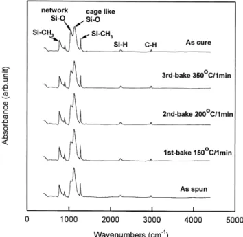
Fig. 1. The FTIR spectra of HOSP films before and after a series of baking and curing steps.
3. Results and discussion
Fig. 1. shows the FTIR spectra of HOSP before and after a series of baking and curing steps. After 150 8C, 200 8C, and 350 8C baking, the intensity of Si–O (cage) peak signal is decreased and Si–O–Si (network) peak intensity is increased. After 400 8C curing, the network structure appeared sig-nificantly. It is shown clearly that a large amount of Si–O bonds crosslink into Si–O–Si bonds and form a more rigid network structure.
In the integration processes, photoresist stripping is the indispensable step to remove organic elements. The photoresist removal is implemented conventionally by utilizing O plasma ashing and2 wet stripper solution treatment. Therefore, the impact of O plasma and chemical wet stripper on the2 quality of HOSP film must be investigated. Fig. 2 shows the FTIR spectra of the as-cured HOSP film before and after photoresist stripping process. Si–OH and H–OH bonds appear after photoresist stripping. Furthermore, the intensity of Si–H, C–H and Si–CH3 peak signals are also decreased dramatically.
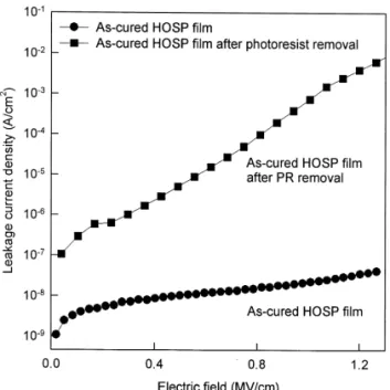
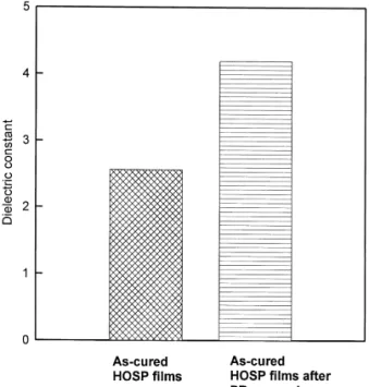
Fig. 3 shows the leakage current density of the HOSP films before and after the photoresist stripping process. The leakage current of HOSP film is increased after photoresist stripping, and furthermore the dielectric constant is also increased after photoresist stripping, as shown in Fig. 4.
No matter electrical measurement or material analysis, these results show that film degradation occurs in the HOSP films after photoresist removal. During O plasma ashing, Si–CH bonds and2 3 Si–H bonds in HOSP film will be broken by oxygen radicals attack. The broken Si–H, C–H and Si–CH3 bonds will form the dangling bonds, leading to the unstable film. Sequentially, the high-alkalinity content of wet stripper solution (pH512.6) lead to a continuous hydrolysis reactions of HOSP films, forming even more dangling bonds. These dangling bonds will react with hydroxide
2
472 T.C. Chang et al. / Microelectronic Engineering 60 (2002) 469 –475
Fig. 2. The FTIR spectra of HOSP films before and after photoresist stripping processes (i.e. O plasma ashing and wet2 stripper dipping).
addition, the Si–OH bonds in the damaged HOSP films often lead to moisture uptake. Hence the leakage current and the dielectric constant will be increased.
For this reason, H plasma is used to treat HOSP film in order to enhance the resistance against2 photoresist stripping damage. Fig. 5 shows the leakage currents density of H plasma-treated HOSP2 films (Samples 3H, 6H and 9H) after photoresist stripping process. The leakage currents of H2
Fig. 4. The dielectric constant of HOSP film before and after photoresist stripping processes.
plasma-treated HOSP films are much lower than that of untreated HOSP film after photoresist stripping. Moreover, the dielectric constants of H plasma-treated HOSP films (Samples 3H, 6H and2 9H) can still maintain stable after photoresist stripping, as shown in Fig. 6.
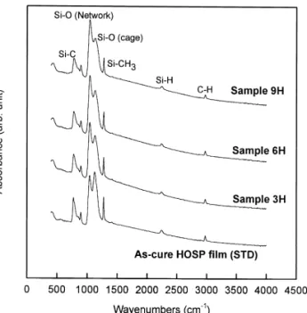
Fig. 7 shows the FTIR spectra of H plasma-treated HOSP films (Samples 3H, 6H and 9H) after2 being undergone photoresist stripping. All the function group signals of the H plasma-treated HOSP2
Fig. 5. The leakage current density of Sample STD, Sample 3H, Sample 6H and Sample 9H after photoresist stripping processes.
474 T.C. Chang et al. / Microelectronic Engineering 60 (2002) 469 –475
Fig. 6. The dielectric constant of Sample STD, Sample 3H, Sample 6H and Sample 9H after photoresist stripping processes. films can be observed and the peak intensity is still maintained at a high level even after photoresist stripping. In addition, the peaks of Si–OH bonds and H–OH bonds do not appear in the FTIR spectra. The dangling bonds in HOSP surface can easily convert to Si–OH bonds, absorbing moisture and lead to the reduction of reliability. The H plasma treatment provides active hydrogen to passivate the2
HOSP surface and forms a thin passivation layer. For this reason, the dangling bond content in HOSP film could be decreased by the H plasma treatment. The thin passivation layer on the HOSP surface2 can enhance the resistibility against moisture uptake. Therefore, the leakage current will decrease and dielectric constant will keep at a low k value when H2 plasma-treated HOSP films undergoes photoresist stripping process.
4. Conclusions
In this work, H plasma treatment to the HOSP film is investigated during photoresist stripping2 processes. The H plasma treatment can passivate the HOSP surface with active hydrogen radicals2 and prevent dielectric loss originating from O plasma and wet stripper processes. Material analyses2 and electric measurements can confirm our inference. The Si–OH bounds do not appear in the FTIR spectra even after H plasma-treated HOSP film undergoes photoresist stripping. It is also found that2 the leakage current of H plasma-treated HOSP films is decreased significantly and the dielectric2 constant are also maintained at a low k value. These results indicate that H plasma treatment is a2 promising technique to enhance the resistance of HOSP film against photoresist stripping damage.
Acknowledgements
This work was performed at the National Nano Device Laboratory and was supported by the National Science Council of the Republic of China under Contract, No. NSC90-2112-M-110-004 and No. NSC90-2215-E-009-048.
References
[1] The National Technology Roadmap for Semiconductors, Semiconductor Industry Association, San Jose, CA, 1997. [2] T.E. Seidel, C.H. Ting, Material Research Society Symp. Proc., Vol. 381, 1995, pp. 3–17.
[3] P.T. Liu, T.C. Chang, Y.L. Yang, Y.F. Cheng, S.M. Sze, IEEE Trans. Electron. Dev. 47 (2000) 1733–1739. [4] M.H. Tsai, W.T. Whang, Polymer 42 (2001) 4197–4207.
[5] M.J. Loboda, Microelectron. Eng. 50 (2000) 15–23.
[6] M.J. Loboda, C.M. Grove, R.F. Schneider, J. Electrochem. Soc. 145 (8) (1998) 2861–2866.
[7] X. Xiao, R. Streiter, H. Wolf, G. Ruan, C. Murray, T. Gessner, Microelectron. Eng. 55 (2001) 53–57.
[8] P.T. Liu, T.C. Chang, H. Su, Y.S. Mor, Y.L. Yang, H. Chung, J. Hou, S.M. Sze, J. Electrochem. Soc. 148 (2) (2001) F30–F34.
[9] P.T. Liu, T.C. Chang, Y.S. Mor, S.M. Sze, Jap. J. Appl. Phys. 38 (1999) 3482–3486.
[10] P.T. Liu, T.C. Chang, S.M. Sze, F.M. Pan, Y.J. Mei, W.F. Wu, M.S. Tsai, B.T. Dai, C. Y Chang, F. Y Shih, H.D. Huang, Thin Solid Films 332 (1998) 345–350.