This content has been downloaded from IOPscience. Please scroll down to see the full text.
Download details:
IP Address: 140.113.38.11
This content was downloaded on 25/04/2014 at 16:10
Please note that terms and conditions apply.
Low cost fabrication of the large-area anti-reflection films from polymer by
nanoimprint/hot-embossing technology
View the table of contents for this issue, or go to the journal homepage for more 2008 Nanotechnology 19 205301
(http://iopscience.iop.org/0957-4484/19/20/205301)
Nanotechnology 19 (2008) 205301 (5pp) doi:10.1088/0957-4484/19/20/205301
Low cost fabrication of the large-area
anti-reflection films from polymer by
nanoimprint/hot-embossing technology
Chia-Jen Ting
1, Meng-Chi Huang
2, Hung-Yin Tsai
2,
Chang-Pin Chou
1and Chien-Chung Fu
2,31Department of Mechanical Engineering, National Chiao-Tung University, Taiwan 2Institute of Nano Engineering and Microsystems, Department of Power Mechanical Engineering, National Tsing-Hua University, Taiwan
E-mail:[email protected]
Received 19 February 2008, in final form 14 March 2008 Published 14 April 2008
Online atstacks.iop.org/Nano/19/205301 Abstract
In this paper, we present a low cost approach to produce large-area polymer sheets with sub-wavelength nanostructures. The fabricated polymer films would have great potentials to attach to optical or solar-cell-related consumer products when anti-reflection/anti-glaring is mandatory. We employed a special electron cyclotron resonance (ECR) plasma process to fabricate the SWSs with large area directly on silicon substrates. Homogeneously distributed nanotips on the full 4 inch silicon substrate were fabricated by using gas mixtures of silane, methane, argon and hydrogen. An Ni–Co metal mold with a hardness of 550 HV was produced through the replication of the Si mold by electroplating. Afterwards, the molding process was applied to manufacture the nanostructures in PMMA plates in large volume. The nanostructures in PMMA plates with aspect ratios of 4 and diameters of 150 nm were fabricated. The
fabricated PMMA sheets could generate the gradient of the refractive indices, absorb the light and greatly reduce the reflectivity. Compared with the PMMA without SWSs, the reflectivity of PMMA with SWSs decreased dramatically from 4.25% to 0.5% at the wavelength of light from 400 to 800 nm.
1. Introduction
In recent years, anti-reflection layers made from sub-wavelength structures (SWSs) have been extensively studied due to the emerging demand of the solar cell markets. Actually, anti-reflection coatings can also be used in consumer electronics such as planar displays, glasses, prisms, videos and camera monitors. Traditionally, this anti-reflection layer was produced by multilayer film deposition through sputtering, wet-coating or sol–gel. However, these methods have several disadvantages such as process instability, high cost and high temperature procedures.
Tapered SWSs on silicon have been fabricated through different methods. In 1999, the SWSs were manufactured by Kanamori et al [1]. They employed an e-beam writer
3 Present address: No. 101, Kuang-fu Road, Section II, Hsinchu 300, Taiwan, Republic of China.
to generate triangular structures in the photoresist (PR) and utilized a focused SF6 fast atom beam (FAB) to produce
tapered SWSs in the silicon. They also provided another method to generate triangular structures. An Al sheet was anodized by the anode treatment of electrochemistry to generate a nanoporous alumina membrane. An ordered anodic porous alumina (OAPA) membrane had been used as an etching mask. The Si surface was etched by the SF6
FAB and the Si surface was tapered periodically by over-etching [2]. In 2000, Wassermann et al employed laser interference lithography to generate nano-PR patterns on the Si substrate with large area. This pattern was transferred to the substrate by reactive-ion etching [3]. In 2003, Chou et al employed a property of the bad step coverage of an e-gun evaporator under very high aspect ratio PR structures to generate triangular metal patterns as a reaction ion etching (RIE) mask for silicon. Since the substrate and the metal
Nanotechnology 19 (2008) 205301 C-J Ting et al
were slowly eroded away during the RIE, tapered 1D or 2D gratings could be created through a prolonged etching [4]. In 2003, Chen et al provided a method to achieve the formation of nanomasks and etching of nanotips in one step. The SWSs were fabricated using an electron cyclotron resonance (ECR) plasma reactor, in which gases such as hydrogen (H2), argon
(Ar), methane (CH4) and silane (SiH4) were applied [5].
Most researchers so far focused on creating the SWSs on silicon, glass or GaN substrates to produce the anti-reflection performance [1–7]. However, for low cost optical applications, especially for the consumer optical products like anti-glaring mirrors, soft display related products or even solar cells, it is necessary to reduce the process complexity and, at the same time, to keep the possibility to make it in large volume. Adding nanoimprinting/hot-embossing technology to this field would offer an efficient way to resolve the ‘large-area’ and ‘low cost’ problems.
Nanoimprint lithography (NIL) was mentioned for the first time by Chou et al [8]. NIL is a parallel process lithography technique, based on molding of a soft polymer by a hard stamp. It is capable of replicating patterns with a linewidth below 10 nm in a parallel manner [9]. Nanotechnology applications based on NIL have been developed and applied to data storage, opto-electronics and the integrated circuit industry.
In this work, we applied thermoplastic PMMA films, which had a glass transition temperature (Tg) in the range of
100–110◦C. We fabricated tapered SWSs in 4 inch size by ECR plasma based on the method first published in [5]. Then we produced an Ni–Co metal mold with a hardness of 550 HV through the replication of the Si mold by an electroplating process in order to increase the mold robustness. Afterward, the Ni–Co mold was used as the mother mold to transfer SWSs onto the PMMA films.
SWS PMMA films with large area were successfully manufactured. We found that the reflectivity of the PMMA with high-aspect-ratio SWSs was dramatically decreased from 4.25% to 0.5% at the wavelength of light from 400 to 800 nm. This value of reflectivity is comparable with the value (<1.1%) guaranteed by a 3M commercial anti-reflection film [10].
This paper successfully demonstrated a feasible low cost way to produce polymer sheets with sub-wavelength tip structures. The fabricated polymer sheets would have great potential to attach to consumer optical products when anti-reflection/anti-glaring is mandatory.
2. The process
An ECR plasma etcher (Astex Co. Lt., Model: AX 4400) was employed to generate the plasma needed. The gas mixture used in our experiments was silane, methane, argon and hydrogen with a flow rate ratio of 0.2:2:3:8. Nanoscale SiC clusters were generated in the plasma chamber and deposited on the silicon surface as nanomasks. Afterwards, the silicon was etched by an RIE-like process through argon ions. In our experiments, the microwave power was set to be 1200 W. The chamber pressure was set to be 5.8 mTorr. Substrate temperature was controlled to be under 250◦C. According to our experiments, large-area sub-wavelength structures can be generated within 3 h. It takes
much shorter time than using an e-beam writer. The principle of the ECR plasma process was described in [5].
In order to produce the Ni–Co mold, a nickel substrate was used as anode and the silicon substrate with SWSs was used as cathode. Both were immersed in a bath of nickel sulfamate(Ni(NH2SO3)2·4H2O) and cobalt sulfamate (Co(NH2SO3)2·5H2O). A current density of 0.05 A dm−2was
applied for the first 2 h. Then we increased the current density to 0.5 A dm−2for 18 h. The Ni–Co mold containing the SWSs with a depth of 150µm was then produced.
2 mm thick PMMA sheets with a molecular weight of 950 kg mol−1 with a glass transition temperature of 105◦C were used as the workpieces in the hot-embossing step. The PMMA films were hot-embossed at a temperature of 110, 135 and 160◦C with a pressure of 0.6 kg cm−2using an embossing machine (Jenoptik AG, HEX-01). The de-molding temperature of 30◦C was utilized in our experiments. The morphologies of the Si with the generated SWSs and the fabricated PMMA films were measured through a field emission SEM (Hitachi, S-4200). The reflectivity was measured by a spectrophotometer (Jasco International Co. Lt., Model V-570) at the wavelength range from 400 to 800 nm.
3. Experimental results and discussions
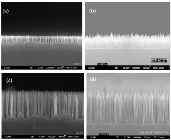
The SWSs on the Si substrates fabricated by the ECR plasma process were shown in figure 1. The diameters of the nanostructures on the Si substrates were 100–150 nm. The heights were 300–1200 nm. The aspect ratios were 2–8. The widths, heights and pitches of the nanostructures could be controlled by the gas volume of the ECR plasma and the etching time.
The Ni–Co mold was also successfully fabricated as shown in figure2. The total thickness of the Ni–Co mold was 150µm after being electroformed for 20 h. The diameters of the nanostructure holes in the Ni–Co mold were from 100 to 150 nm and the heights were from 600 to 800 nm.
Figure 3 shows the SEM images of the PMMA film surface after the hot-embossing process at the temperature of 110, 135 and 160◦C, respectively. The PMMA flowed into the holes of the Ni–Co mold with great difficulty at 110◦C because the temperature was close to the glass transition temperature of the PMMA employed. This low mobility caused the incomplete filling of the nanostructures with a low aspect ratio of about 1.2–1.6.
When the molding temperature increased to 135◦C, the aspect ratios of nanostructures were increased to 2.6–3.0, larger than the aspect ratios at 110◦C. When the temperature increased to 160◦C, the aspect ratios of 4–5.3 could be achieved. The heights of the structures were 480–600 nm.
In figure3(c), the nanostructures looked bendy. This is because, due to the bombardment by electron beams in the SEM, the nanotips got softened and became bendy. They had been very sharp right after they had just been manufactured.
Comparisons of the geometries of SWS in Si mold, Ni– Co mold and PMMA sheets were listed in table 1. There was almost no distortion in the diameter. The diameter of the nanostructures were almost the same in the above three cases. 2
Figure 1. SEM images of nanotip arrays on silicon substrate with different heights (side view): (a) 320 nm, (b) 650 nm, (c) 907 nm, (d) 1240 nm.
Figure 2. SEM image of Ni–Co mold after electroforming process (top view).
The depth of nanoholes in the Ni–Co mold was only about half the height of the SWSs in the Si mold. The heights of PMMA nanotips was very close to the depth of the Ni–Co mold after the hot-embossing process when the processing temperature was set to be 160◦C.
Figure 4 shows the measured reflectivity on the Si substrates as a function of the wavelengths. Compared with the bare Si, the reflectivity of the Si substrate with SWSs was reduced from 50% to 5% at the wavelengths between 400 and 800 nm. SWSs with high aspect ratio and the shapes of tapered
Table 1. Comparisons of the geometries of the SWSs after different processes. Diameter of nanotip/diameter of hole size (nm) Height of nanotip/depth of hole (nm) Aspect ratio Nanotips of silicon (before electroforming) 100–150 1000–1200 ∼6.67–8 Hole of Ni–Co mold
(after electroforming) 100–150 600–800 ∼4–5.33 Nanotips of PMMA at 160◦C (after hot-embossing) 100–150 480–600 ∼3.4–4
angles could absorb the lights and decrease the reflectivity dramatically.
The reflectivity of the PMMA films with SWSs was measured as shown in figure 5. The reflectivity of PMMA without SWSs was about 4.25–4.5% at the wavelength from 400 to 800 nm. The reflectivity of the PMMA films fabricated with the hot-embossing temperature of 160◦C was lower than 0.5%.
The reflectivity was measured as a function of the incident angle as shown in figure 6. The PMMA sheets with SWSs with the aspect ratio of 4 were measured at different incident angles from 5◦ to 60◦ with the wavelength of 550 nm using polarized light. The reflectivity of the PMMA surface was in the range from 0.45 to 0.65 % at incident angles from 5◦to 40◦.
Nanotechnology 19 (2008) 205301 C-J Ting et al
Figure 3. SEM images of PMMA films with SWSs after the hot-embossing process at different molding temperatures of (a) 110◦C; (b) 135◦C; (c) 160◦C.
The reflectivity increased rapidly from 0.65 to 1.2% when the incident angles exceeded 60◦. This was because the gradient of the effective refraction index between the structure material and the air was difficult to be generated when the incident angles exceeded 60◦. This phenomenon can also be found in the paper [1].
Figure 7 showed a comparison between a bare PMMA sheet and the PMMA sheet with SWSs used as the cover of a bulletin window. The result showed an obvious damping of the glaring from the backlight.
4. Conclusion
In this paper, we presented a low cost way to produce polymer sheets with sub-wavelength structures. The fabricated polymer films would have great potential to attach to consumer optical products when anti-reflection/anti-glaring is mandatory.
Figure 4. The reflectivity measured as a function of the wavelengths on SWSs Si surfaces with different heights.
Figure 5. The reflectivity of 2 mm thick PMMA sheets with/without SWS fabricated with different molding temperatures from 110 to 160◦C.
Figure 6. The reflectivity of the fabricated PMMA sheet measured as a function of the incident angles at the wavelength of 550 nm.
We employed a special electron cyclotron resonance (ECR) plasma process to fabricate the SWSs with large area directly on silicon substrates. Homogeneously distributed nanotips on the full 4 inch silicon substrate were fabricated by using gas mixtures of silane, methane, argon and hydrogen. An Ni–Co metal mold with a hardness of 550 HV was then produced through the replication of the Si mold by an 4
Figure 7. The comparison between a bare PMMA sheet and the PMMA sheet with SWSs used as the cover of a bulletin window. It shows an obvious damping of the glaring from the backlight.
electroplating process. Afterwards, the molding process was applied to manufacture the nanostructures in PMMA plates in large volume. The nanostructures in PMMA plates with
aspect ratios of 4 and diameters of 150 nm were achieved. The fabricated PMMA sheets could produce the gradient of the refractive indices, absorb the light and greatly reduce the reflectivity. Compared with the PMMA without SWSs, the reflection of PMMA with SWSs decreased dramatically from 4.25% to 0.5 % at the wavelength of light from 400 to 800 nm.
References
[1] Kanamori Y, Sasaki M and Hane K 1999 Opt. Lett. 24 1422 [2] Kanamori Y, Hane K, Sai H and Yugami H 2001 Appl. Phys.
Lett.78 142
[3] Hadob’as K, Kirsch S, Carl A, Acet M and Wassermann E F 2000 Nanotechnology11 161
[4] Yu Z, Gao H, Wu W, Ge H and Chou Y J 2003 J. Vac. Sci.
Technol. B 6 2844
[5] Lo H C, Das D, Hwang J S and Chen K H 2003 Appl. Phys.
Lett.18 1420
[6] Lin G, Chang Y, Liu E, Kuo H and Lin H 2007 Appl. Phys.
Lett.90 181923
[7] Lin G, Lin C, Kao H, Lin H and Kao C 2007 Appl. Phys. Lett. 90 143102
[8] Chou S Y, Krauss P R and Renstrom J 1995 Appl. Phys. Lett. 67 3114
[9] Boerner V, Abbott S, Bl¨asi B, Gombert A and Hoßfeld W 2003
SID. Symp. Digest34 68
[10] Product Manual of 3M Vikuititmanti-reflection films, from www.3M.com