國
立
交
通
大
學
電子工程學系 電子研究所
博 士 論 文
藉助催化金屬與元件結構以增進奈米碳管場發
射特性之研究
Study on the Improvements of Field-Emission
Characteristics of the Carbon Nanotubes via
Modifying the Catalyst and Device Structures
研 究 生:賴瑞霖
Rui-Ling Lai
指導教授:鄭晃忠 博士 Dr. Huang-Chung Cheng
藉
藉
助
助
催
催
化
化
金
金
屬
屬
與
與
元
元
件
件
結
結
構
構
以
以
增
增
進
進
奈
奈
米
米
碳
碳
管
管
場
場
發
發
射
射
特
特
性
性
之
之
研
研
究
究
Study on the Improvements of Field-Emission Characteristics of
the Carbon Nanotubes via Modifying the Catalyst and Device
Structures
研 究 生
: 賴瑞霖 Student : Rui-Ling Lai
指導教授
: 鄭晃忠 博士 Advisor : Dr. Huang-Chung Cheng
國立交通大學
電子工程學系 電子研究所
博士論文
A Dissertation
Submitted to Department of Electronics Engineering
and Institute of Electronics
College of Electrical and Computer Engineering
National Chiao Tung University
In Partial Fulfillment of the Requirements
for the Degree of
Doctor of Philosophy
in Electronics Engineering
2006
Hsinchu, Taiwan, Republic of China
藉助催化金屬與元件結構以增進奈米碳管場發射特
性之研究
研究生:賴瑞霖 指導教授:鄭晃忠 博士
國立交通大學電子工程學系暨電子研究所博士班
摘要
在本篇論文當中,我們利用奈米碳管為場發射元件之電子源,並藉由改善催化金 屬材料及其元件結構以改善場發射特性。於此研究中,我們運用金屬鈦覆蓋或摻雜於 催化金屬鐵以控制催化金屬之活性、大小以及分佈,進而增進場發射電流密度、增強 元件可靠度或是改善場發射電流之均勻性。此外,我們亦藉由微影的方式製作柱狀之 奈米碳管場發射源,藉由人造結構來得到均勻之場發射電子源分佈,並有效控制柱狀 場發射源之間距以降低電場遮蔽效應,而得到最佳化之場發射電流以及啟始電場。最 後,於三極場發射元件中加入一層氮化矽以阻絕閘極與陰極間之漏電,進而改善三極 場發射元件效率不佳之缺點。 首先,在場發射電流密度方面,對於奈米碳管而言,影響其電流密度之主要原因 在於過高的奈米碳管密度所導致的電場屏蔽效應。對此,我們在經過氫氣前處理之鐵 奈米顆粒上沈積一層微薄之金屬鈦,藉助鈦阻擋含碳之反應物質進入鐵催化金屬進而 抑制奈米碳管之生成以降低奈米碳管的密度。藉由沈積不同厚度之金屬鈦,我們可以 有效地控制奈米碳管之密度以增進其場發射電流密度並降低其啟始電場。此外,藉由 所沈積之金屬鈦在奈米碳管成長過程中受熱部分融化並包圍鐵催化金屬奈米顆粒,我們發現元件在量測過程所發生之電流崩潰現象有效地被抑制了,而其場發射電流在高 電場下之劣化現象亦有效地被改善,針對此一結果,我們認為金屬鈦之包圍使得奈米 碳管與基板之間的附著性被增強且降低其接觸電阻,因此改善了元件的可靠度。 然而,雖然電流密度與可靠度被改善了,其均勻性不佳之現象依然無法得到解決, 是以我們利用金屬鈦與催化金屬鐵共鍍作為成長奈米碳管之催化金屬層,藉此使催化 金屬顆粒之形成更為均勻,並藉由金屬鈦抑制催化金屬顆粒的聚集以得到小尺寸、且 尺寸均勻之催化金屬奈米顆粒,最後成長出長度均勻之奈米碳管並在塗佈螢光粉之陽 極板上得到均勻之光源。此外,因為鐵催化金屬顆粒於催化金屬層中受熱析出而形成 部分被埋於催化金屬層中之結構,其可靠度亦大為改善。 接著,我們利用微影的方式以鐵鈦共鍍為催化金屬製作柱狀奈米碳管之場發射元 件。藉由鐵鈦共鍍以得到均勻、筆直且具有穩定場發射電流之奈米探管;利用微影控 制其間距,以有效降低電場屏蔽效應並且避免距離過大而減少場發射區域之總面積。 是以,得到一個均勻分佈且具有較高場發射電流密度之場發射電子源。 最後,針對三極式場發射電子元件效率不佳之缺點,我們在元件中增加一層氮化 矽絕緣層於閘極之上或閘極之下,以阻絕由陰極被閘極電場所吸引出來的電子電流, 藉此改善電流效率以及功率效能。 在本論文中,我們提出了簡單、便宜且不會對場發射源奈米碳管造成結構損傷之 方式來改善場發射電子元件之場發射特性。是以相當具有應用於場發射平面顯示器或 是液晶螢幕背光模組之潛力。
Study on the Improvements of Field-Emission
Characteristics of the Carbon Nanotubes via
Modifying the Catalyst and Device Structures
Student: Rui-Ling Lai Advisor: Dr. Huang-Chung Cheng
Department of Electronics Engineering & Institute of Electronics
College of Electrical Engineering and Computer Science
National Chiao Tung University
ABSTRACT
In this dissertation, the carbon nanotubes (CNTs) were utilized as the electron source in field-emission devices. By modifying the metallic catalysts and the device structures, the field-emission characteristics were greatly improved. In this research, Ti capping layer and Ti codeposited with Fe were used to control the activity, size, and distribution of the Fe catalytic nanoparticles for improving the emission current density, reliability, and uniformity of the devices. Moreover, the diameter and position of pillar-like CNTs synthesized from Fe-Ti codeposited catalyst were controlled by lithography. Therefore, a uniform distribution of emitters with suppressed screening effect was obtained for high emission current density and low turn-on field. Finally, a silicon nitride film was added into the triode-type field-emission devices to block the leakage current between the gate and the cathode for improving the power efficiency.
For emission current density, the high density of CNTs caused a serious screening effect which could greatly decrease the emission current density. Accordingly, a thin Ti
capping layer was deposited on the hydrogen pretreated Fe nanoparticles to resist the diffusion of the carbon radicals and effectively reduce the density of emitters. By altering the thickness of the Ti capping layer, a suitable density of CNTs was obtained with high emission current density and low turn-on field. Moreover, the Ti capped on the Fe nanoparticles held the nanoparticles firmly to provide stronger adhesion and lower contact resistance than those synthesized from the pure Fe. It remarkably suppressed the breakdown of the field-emission devices and diminished the degradation of emission current density at high electric field. It might result from the improvements of the contact properties with the modification of metallic catalyst.
However, the problems of uniformity were still not solved by means of the thin Ti capping layer. Therefore, a Fe-Ti codeposited metal layer was utilized as the catalyst of CNTs. During being heated, the nucleation of Fe atoms formed smaller nanoparticles with better uniformity due to the suppression of coalescence between Fe nanoparticles than those synthesized from pure Fe. A homogeneous light emission was therefore observed on the phosphor (P22) coated glasses. Furthermore, the nucleation of Fe nanoparticles resulted in a partially immersed structure of the CNTs which provided better contact properties between the CNTs and the substrates. As previous description, the reliability of the device could be improved.
Additionally, the lithography was utilized to form an artificial structure of pillar-like CNTs to control the diameter and distribution of emitters more precisely. The Fe-Ti codeposited catalyst was utilized for uniform CNTs with reliable emission current. A uniform distribution of emitters with low turn-on field was therefore achieved.
Finally, a silicon nitride layer was deposited on the poly-gate or under the poly-gate to block the electron emission from the cathode to the gate. Both of them could effectively improve the current efficiency and therefore increase the power efficiency of triode-type field-emission devices.
In this dissertation, simple, costless, and harmless methods have been proposed to improve the field-emission characteristics of CNTs. It showed a great potential in the applications of the field-emission displays and the back-light units in near future.
誌 謝
首先,要感謝我的指導教授 鄭晃忠 博士,在研究上給予我諄諄教誨,並適時地 給予我專業的建議,使我能更清楚自己研究的目標與方向;此外,老師也時時關心我 研究外生活的情況,常常教導我待人接物的道理,令我獲益良多,使我能順利地完成 學業並獲得博士學位。也感謝在百忙之中抽空參加我論文口試的委員們,有了委員們 專業的建議與熱心的指導,才能使我的論文更加地完整。 感謝實驗室的學長、同學以及學弟妹在生活上以及研究上的協助,令我在交通大 學的學生生活更加地豐富也更加地順遂。鼎國學長在研究上的經驗談以及日常生活中 的相處令我受惠良多;國基學長、全平學長以及高照學長在相關實驗上的經驗傳承以 及教導令我能更順利地進行相關的研究;感謝耀仁學弟、鈞凱學弟以及佩琪學妹的協 助,共同在場發射元件的相關研究上貢獻心力,因為你們的付出才有今天的成果。也 感謝宗穎學弟、翰忠學弟、俠威學弟、建穎學弟、君翰學弟、育瑛學妹各位同組的成 員在實驗上給予我建言與協助。 除此之外,也感謝交通大學奈米中心以及國家奈米實驗室能提供我最先進、最優 良的實驗環境與設備。也感謝親切可愛的技術員徐秀巒小姐、黃月美小姐、范秀蘭小 姐、鄭淑娟小姐、陳聯珠小姐、陳月婷小姐以及胡進章先生在技術上的協助,以及行 政人員劉曉玲小姐與何惟梅小姐在行政事物上的協助。 還要感謝春乾學長、國瑞學長、逸哲學弟、育如學妹、可玉學妹、大傳學弟、瑛 君學妹、旭信學弟、凱方學弟、祐圻學弟、心瑜學妹、仕偉學弟、序恆學弟以及偉凱 學弟…等等實驗室成員在研究上以及生活上的協助。因為有了大家,才令我的論文能 順利完成,生活才更加的豐富多姿。 最後,僅以此篇論文獻給我最敬愛的父母-賴德曙先生以及陳麗貞女士,因為父母 的悉心栽培才能有今天的我,感謝他們在生活上令我無虞,隨時隨地支持我、鼓勵我, 令我能有決心與毅力完成學業。也感謝我的女朋友以及妹妹,無時不刻給予我溫暖的關懷,令我在灰心、氣餒的時候不被眼前的困難所打倒。
最後感謝身邊所有的親朋好友,謝謝你們一路以來的相挺以及協助,因為有了你 們的關懷我才能順利完成博士學位,有機會我一定會請你們吃雞排加紅茶的(希望大家 在得知我畢業的消息時不要太殘忍)。
Contents
Abstract (in Chinese)...i
Abstract (in English)...iii
Acknowledgments (in Chinese)...vi
Contents...viii
Table Lists...xii
Figure Captions...xiii
Chapter 1 Introduction
1.1 Overview of Vacuum Microelectronics...1
1.1.1 Technologies of Vacuum Microelectronics...3
1.1.2 Applications of Vacuum Microelectronics in Field-Emission
Displays...11
1.2 Theory of Field Emission...13
1.3 Carbon Nanotubes...17
1.3.1 Arc discharge...18
1.3.2 Laser Ablation...18
1.3.3 Chemical Vapor Deposition...18
1.4 Motivation...20
1.4.1 Reliability...20
1.4.2 Uniformity...21
1.5 Outline of Dissertation...21
Reliability for the CNTs Synthesized from the Ti-Capped Fe
Nanoparticles
2.1 Introduction...23
2.2 Experimental Procedures...26
2.2.1 Sample Fabrication...26
2.2.2 Material Analysis and Electrical Measurement...28
2.3 The Emission Current Density of the Carbon Nanotubes Synthesized
from a Ti Capped Catalytic Nanoparticles...28
2.4 The Reliability Improvements of the Carbon Nanotubes by Modifying
the Contact Properties...32
2.5 Summary...35
Chapter 3 The Improvements of Reliability and Uniformity for
the CNTs Synthesized from the Fe-Ti Codeposited Catalyst
3.1 Introduction...37
3.2 Experimental Procedures...39
3.2.1 Sample Fabrication...39
3.2.2 Material Analysis and Electrical Measurement...40
3.3 The Partially Immersed Structure of the Carbon Nanotubes for the
Reliability Improvements...41
3.4 The Suppression of the Coalescence between Fe Nanoparticles for a
Uniform Light Emission...45
Chapter 4 The Synthesis and Characteristics of the Pillar-Like
CNTs Synthesized from the Fe-Ti Codeposited Catalyst
4.1 Introduction...49
4.2 Experimental Procedures...50
4.2.1 Sample Fabrication...50
4.2.2 Material Analysis and Electrical Measurement...52
4.3 The Synthesis of the Pillar-Like Carbon Nanotubes by Utilizing the
Fe-Ti Codeposited Catalyst...52
4.4 The Optimization of the Inter-Pillar Spacing Designed via the
Lithography...54
4.5 Summary...56
Chapter 5 The Reduction of Gate Leakage for the CNTs-Based
Triode Devices via Adding a Silicon Nitride Layer
5.1 Introduction...58
5.2 Experimental Procedures...60
5.2.1 Sample Fabrication...60
5.2.2 Material Analysis and Electrical Measurement...61
5.3 The Power Efficiency Improvements via Cutting Off the Leakage
Paths...61
5.4 Summary...62
Chapter 6 Summary and Conclusions
...64
Chapter 7 Future Prospects
...67
References
...69
Tables
...92
Figures
...98
Vita
...197
Publication Lists
...198
Table Lists
Chapter 1
Table 1.1 The timeline for the evolution of electronic technology...90
Table 1.2 The comparison of several flat panel displays...91
Table 1.3 The history of vacuum microelectronics...92
Table 1.4 The features of different field-emission technologies...93
Chapter 2
Table 2.1 The turn-on field and threshold field of samples with different thickness of Ti capping layer...94Table 2.2 The densities of CNTs for samples with different thicknesses of Ti capping layer...94
Chapter 4
Table 4.1 The turn-on field and threshold field of the pillar-like CNTs with different intespacing...95Figure Captions
Chapter 1
Figure 1.1 The scheme of Spindt-type field emitter arrays. The height of the cones and thickness of the dielectric layer are both about 1 μm, the tip radius is about 20 nm, the gate aperture is about 0.5 μm, and the tip-to-tip spacing is about 1~5 μm...96 Figure 1.2 The processes of fabricating Spindt field emitter arrays: (a) etch cavities in the
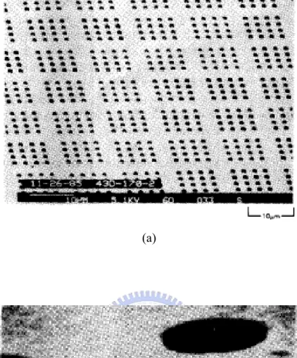
top two layers of a metal/dielectric/metal stack were formed by lithography and subsequent wet or dry etching, (b) a sacrificial lift-off layer is deposited onto the top layer and inner walls of the upper portion of the cavity by a tilted deposition with rotating the substrate on an axis perpendicular to the surface, (c) form metal cones in the cavities by depositing metal perpendicular to the substrate surface and the tilted deposition can be applied continuously or intermittently during this step to help to control the hole-closure rate and to manage stresses in the deposited layer as desired, and (d) a lift-off process is done by removing the sacrificial layer in a wet etching solution which only attacks the sacrificial layer without damage the metal cones seriously...97 Figure 1.3 The micrographs taken by SEM for (a) Spindt field emitter arrays and (b)
device structure with higher resolution...98 Figure 1.4 The schematic illustration of orientation-dependant etching (ODE) method for
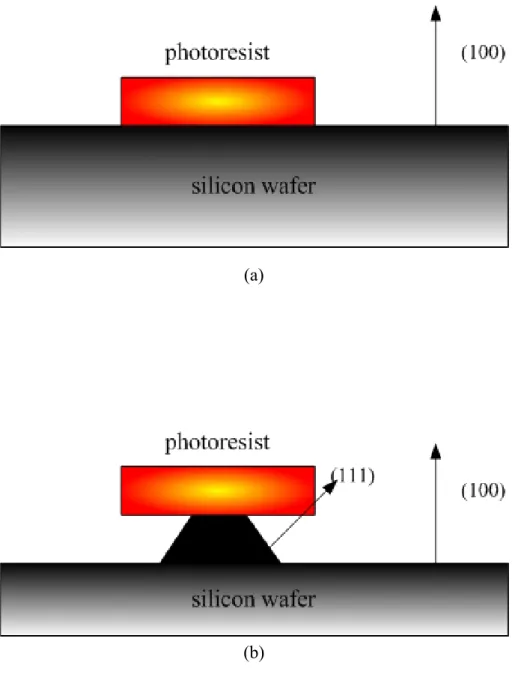
fabricating silicon tips: (a) using lithography to pattern a etching mask to inhibit etching in locations where pyramids are desired and (b) etching of silicon is much faster at the (100) plane than at (111) plane, forming a (111) bounded pyramid in the end...99
Figure 1.5 The flowchart of the oxidation sharpening: (a) depositing a nitride layer on the silicon wafer and form an array of dots via lithography, (b) etch the nitride by dry etching and remove the photoresist, (c) undercut the silicon to form tips under the hard nitride mask by an isotropic etching (wet or dry etching), (d) form sharper silicon tips by oxidation at about 950 °C or lower, and (e) remove the nitride mask and thermal oxide to uncover the sharp silicon tips...100 Figure 1.6 The illustration of surface conduction emitters: (a) the device structure from
top view with two ultrafine PdO films as cathode and gate electrodes and (b) the mechanism of surface conduction emission. A suitable voltage is applied between the two PdO films to extract electrons from cathode to gate and the electrons will be multi-scattered on the surface of PdO then extracted by the anode which is applied at a very high voltage...101 Figure 1.7 The schematic illustration of the ferroelectric emission mechanism. The
screening charges are developed to compensate the net charges and a fast reversal of the polarization results a large electric field that ejects the electrons from the negative charged surface...102 Figure 1.8 The schematic depiction of (a) the MIM device structure and (b) the emission
mechanism...103 Figure 1.9 A schematic illustration for the structures of a cathode-ray tube and a
field-emission display. The left image shows that the electron source in the CRT is far from the anode but the electron source in the FED is just a millimeter away from the anode. The right-side figure demonstrates the cross-section view of a FED...104 Figure 1.10 The device structures of (a) diode-type and (b) triode-type in field-emission
device structure are the gate electrode around the emitter which can extract electrons from the cathodes at relative low electric field...105 Figure 1.11 The energy diagrams demonstrate the mechanisms of (a) thermionic-field
emission and (b) field emission in semiconductor...106 Figure 1.12 The band diagram of the field-emission emitters in the vacuum environment (a)
without applied electric field and (b) with applied electric field...107 Figure 1.13 The structure of the arc discharge system for synthesizing CNTs...108 Figure 1.14 The scheme for the structure of laser ablation system...109 Figure 1.15 The structure of chemical vapor deposition system for synthesizing CNTs..110
Chapter 2
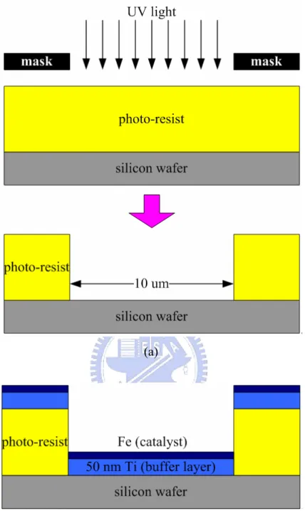
Figure 2.1 The schematic flowchart for the fabrication of experimental samples: (a) forming a 50×50 array of square holes with 10 µm in length and 10-um inter-space by the lithography system, (b) depositing a 50-nm-thick Ti buffer layer and a 5-nm-thick Fe catalytic layer subsequently by the dual-electron-gun deposition system, (c) removing the photoresist with Ti buffer layer and Fe catalytic layer by a lift-off process, (d) loading the samples into the thermal-CVD to be pretreated in hydrogen and form Fe nanoparticles, (e) depositing a thin Ti capping layer with 1 to 20 nm in thickness by the dual-electron-gun deposition system, and (f) synthesizing CNTs in the thermal-CVD...111 Figure 2.2 The samples were put on a glass substrate with a spacer of about 100 μm from
the CNTs to the anode and the anode was a glass coated with a indium-tin-oxide (ITO) film and green phosphor (P22). The samples were loaded into a vacuum chamber with anode applied to the high-voltage source measurement unit, Keithley 237, and the cathode applied to the high-current
source measurement unit, Keithley 238, to measure the field-emission current at high vacuum environment...113 Figure 2.3 The pictures shown here were the images taken by SEM for the Fe
nanoparticles that have been pretreated in hydrogen ambient for 5 min in the thermal-CVD with different thicknesses of the thin Ti capping layer: (a) 0 nm, (b) 1 nm, (c) 2 nm, (d) 4 nm, (e) 10 nm, and (f) 20 nm. With thicker Ti capping layer, the Fe nanoparticles were getting obscure in the micrographs due to being buried in the Ti capping layer...114 Figure 2.4 The surface morphologies taken by the SEM from top with 45° viewing angle
for the CNTs of the samples with different thicknesses of the Ti capping layer: (a) 0 nm, (b) 1 nm, (c) 2 nm, (d) 4 nm, (e) 10 nm, and (f) 20 nm. It was obvious that the number density of the CNTs was decreased with the increasing thickness of the Ti capping layer...117 Figure 2.5 The scheme for the conditions of the Fe nanoparticles capped with thin Ti
capping layer after being heated at 700 °C during the synthesis of the CNTs in the thermal-CVD: (a) the Fe nanoparticles capped with the thin Ti capping layer before growing the CNTs, (b) the deposited thin Ti capping layer was partially melted and getting thinner during the synthesis of CNTs at 700 °C, and (c) part of the Fe nanoparticle might even be exposed during the heating at 700 °C...120 Figure 2.6 The morphologies of CNTs synthesized with different materials as the capping
layer: (a) Mo, (b) Ti, (c) Al, and (d) without capping layer...122 Figure 2.7 The SEM images of CNTs with different thickness of thin Ti capping layer
from the top view: (a) 0 nm (b) 1 nm (c) 2 nm (d) 4 nm (e) 10 nm (f) 20 nm...124 Figure 2.8 The field-emission characteristics for the samples with different thicknesses of
the Ti capping layer: (a) the emission current density versus the electric field and (b) the F-N plot...127 Figure 2.9 The Raman spectra of the CNTs with no Ti capping layer and with Ti capping
layer of 1 nm and 2 nm. The Raman spectra for the samples with thicker Ti capping layer were too weak to be detected here...128 Figure 2.10 (a) The micrograph of the CNTs taken by TEM and (b) The micrograph of
CNTs taken by TEM with higher resolution...129 Figure 2.11 The analysis results of energy dispersive spectrometer for the nanoparticles
enclosed in CNTs as shown in Fig. 2.10(a)...131 Figure 2.12 The emission current density versus electric field for the samples without Ti
capping layer (the conventional samples)and the samples with 5-nm-thick Ti capping layer (the proposed samples). An abrupt decrease in emission current density was observed in the conventional samples and no obvious decrease in emission current density was observed in the proposed samples. After the breakdown in the conventional samples, almost no emission current density was measured in the second measurements...132 Figure 2.13 The micrographs taken by the SEM for (a) the morphologies of the CNTs in
the conventional samples after the electric breakdown and (b) the image with higher resolution...133 Figure 2.14 (a) the emission current density of both the conventional and the proposed
samples over one hour (the emission current density of the conventional samples in the first 6 sec was removed) and (b) the emission current density of the conventional samples for the first 6 sec...134
Chapter 3
length and 100 µm interspacing were patterned by the lithography system on a photoresist film, (b) a 50-nm-thick Ti layer was deposited by the dual-electron-gun physical vapor deposition system and a catalytic metal layer (Fe-Ti codeposited layer for proposed samples and pure Fe for conventional samples) was subsequently deposited in the same chamber, (c) the photoresist was remove by a lift-off process in acetone solution to leave the Ti buffer layer with the catalyst in the squared holes only, (d) loaded into the chamber of thermal-CVD to be pretreated in hydrogen ambient (H2/N2 = 400/600 s.c.c.m.)
at 700 °C for 5 min, and (e) grew the CNTs in the same chamber with ethylene (C2H4/H2/N2 = 5/100/10 s.c.c.m.) at 700 °C for 15 min...135
Figure 3.2 The images of SEM displayed the roots of the CNTs for both (a) the conventional specimens and (b) the proposed specimens with high resolution. The proposed specimens were cleaved across the patterned area and a CNT partially immersed into the codeposited metal layer on the cleaved edge was marked by a circle in (c)...137 Figure 3.3 The micrographs of the CNTs synthesized from the Fe-Ti codeposited catalyst
taken by the TEM: (a) a CNT with an enclosed nanoparticle and (b) the multiwalled structure of the CNTs with higher resolution...139 Figure 3.4 The phase diagram of Fe-Ti...141 Figure 3.5 The results of energy dispersive spectrum for the enclosed nanoparticle in Fig. 3.8(a) where only signals of Fe, C, and Cu were detected...142 Figure 3.6 The Raman spectrum of the CNTs in the conventional samples and the
proposed samples...143 Figure 3.7 The schemes of mechanisms illustrated the formation of nanoparticles during
hydrogen pretreatment and the growth of CNTs for both (a) the conventional specimens and (b) the proposed specimens...144
Figure 3.8 The surface energies of elements...146 Figure 3.9 The curves of emission current density versus electric field from 0 to 7 V/µm
for (a) the conventional samples and (b) the proposed samples before and after being stressed...147 Figure 3.10 The emission current density versus operating time of (a) the conventional
samples and (b) the proposed samples for 2,500 sec...148 Figure 3.11 The micrographs taken by SEM displayed the morphologies of both the
conventional and the proposed samples before and after being stressed...149 Figure 3.12 The micrographs of the catalytic nanoparticles taken by the SEM from
top-view for (a) the conventional samples and (b) the proposed samples...150 Figure 3.13 The atomic force microscope images (scanning area of 10 um× 10 um) of the
catalytic nanoparticles for (a) the conventional samples and (b) the proposed samples...151 Figure 3.14 The micrographs of the CNTs taken by the SEM with 45° viewing angle for (a)
the conventional samples and (b) the proposed samples. The cross-sections of the CNTs taken by the SEM: (c) the conventional samples and (d) the proposed samples. ...152 Figure 3.15 The scheme for the formation of the catalytic nanoparticles in (a) the
conventional samples and (b) the proposed samples...154 Figure 3.16 The curves of emission current density versus applied electric field for both
the conventional and the proposed samples...155 Figure 3.17 (a) The luminescent images for the conventional samples operated at 500 V,
600 V, and 700 V of anode voltages and (b) The luminescent images for the proposed samples operated at 500 V, 600 V, and 700 V of anode voltages....156
Figure 4.1 The flowchart of experimental processes: (a) spin photoresist on N-type silicon wafers and then form a hole-array of circles with 6 µm in diameter and different inter spacing of 12, 15, 20, 25, 30, and 35 µm in a rectangular of 1 mm in width and 2 mm in length, (b) depositing a 50-nm-thick Ti metal as a buffer layer by dual electron-gun physical vapor deposition system and subsequently codeposited a 10-nm-thick Fe and Ti film as the catalyst of CNTs (Fe 64% w.t.), (c) the photoresist was removed by a lift-off process in an ultrasonic cleaner with acetone solution and only Ti buffer layer and Fe-Ti codeposited catalyst were left in the circle holes, (d) the samples were loaded into a thermal-CVD to be pretreated in hydrogen ambient (N2/H2 = 500/100
s.c.c.m.) at 700 °C for 8 min, and (e) finally synthesized CNTs with ethylene (C2H4/N2/H2 = 20/500/100 s.c.c.m.) at 700 °C for 15 min...158
Figure 4.2 The cross-section view of pillar-like CNTs synthesized from the 5-nm-thick pure Fe catalytic film in the thermal-CVD for (a) 8 min, (b) 15 min, (c), 30 min, (d) 60 min, and (e) 120 min...160 Figure 4.3 The cross-section view of pillar-like CNTs synthesized from the Fe-Ti
codeposited catalytic film in the thermal-CVD for (a) 8 min, (b) 15 min, (c), 30 min, (d) 60 min, and (e) 120 min...163 Figure 4.4 The relationship of the length of pillars versus the growth time for both the
conventional and the proposed samples...166 Figure 4.5 The morphologies of the hydrogen pretreated catalytic nanoparticles for both
(a) the conventional samples and (b) the proposed samples...167 Figure 4.6 The scheme of a sphere partially immersed in the substrate...168 Figure 4.7 The surface to volume ratio of sphere in Fig. 5.6 versus the radius and the
angle θ...169 Figure 4.8 The images of CNTs with higher resolution for (a) the conventional samples
and (b) the proposed samples...170 Figure 4.9 The micrographs of the pillar-like CNTs with different interpillar spacing, (a)
12 µm, (b) 15 µm, (c) 20 µm, (d) 25 µm, (e) 30 µm, and (f) 35 µm, taken by SEM with 45 ° viewing angle...171 Figure 4.10 The cross-section views of the pillar-like CNTs with different interpillar
spacing, (a) 12 µm, (b) 15 µm, (c) 20 µm, (d) 25 µm, (e) 30 µm, and (f) 35 µm...174 Figure 4.11 The field-emission characteristics of the pillar-like CNTs (a) the emission
current of samples versus applied voltage and (b) the Fowler-Nordhiem plot of each samples...177 Figure 4.12 The curve of the turn-on field versus the interpillar spacing for the pillar-like
CNTs with different interpillar spacing...178 Figure 4.13 The average of the emission current density for all the samples with different
interpillar spacing applied at 800 V for 1 hour...179 Figure 4.14 The luminescent image of the pillar-like CNTs applied at 800 V taken by
digital camera...180
Chapter 5
Figure 5.1 The scheme of device structures in field-emission displays for (a) the diode-type and (b) the triode-type...181 Figure 5.2 (a) The flowchart of the conventional samples, (b) The flowchart of the OPN
(oxide-poly-nitride) samples, and (c) The flowchart of the ONP (oxide-nitride-poly) samples...182 Figure 5.3 The device structures of the (a) conventional samples, (b) the OPN
(oxide-poly-nitride) samples, and (c) the ONP (oxide-nitride-poly) samples...190
Figure 5.4 The vacuum measurement structure of the triode-type field-emission devices...191 Figure 5.5 The cross-section views of (a) the conventional samples, (b) the OPN
(oxide-poly-nitride) samples, and (c) the ONP (oxide-nitride-poly) samples taken by SEM. The insets were top views with 45° viewing angle for those samples that have undergone the process of CNTs synthesis...192 Figure 5.6 The emission current density of anode versus gate voltage for the conventional
samples, the OPN samples, and the ONP samples...193 Figure 5.7 The leakage current paths between gate and cathode in (a) the conventional
Chapter 1
Introduction
1.1
Overview of Vacuum Microelectronics
The invention of vacuum tubes can be traced back to the observation of emission current by the research team of Thomas Edison during the experimental processes of finding proper materials for light bulb filament in early 1880. Although Thomas Edison could not figure out the mechanism of emission current passing through the evacuated bulb, he still filed a patent with no application purpose and, therefore, this phenomenon was also called “Edison Effect” nowadays. Until 1905, the first electronic diode vacuum tube was designed and fabricated by an English physicist, John Ambrose Fleming, and became a vital unit in radio receivers and radars for many decades afterwards. In 1906, an American electrical engineer, Lee De Forest, added a control “grid” into the Fleming diode to control the emission current between the cathode and the anode. It was the prototype of vacuum triode where a small voltage signal applied on the control grid can be amplified to be a large signal on the anode electrode with great linearity and large voltage swing. It was very essential in the creation of long-distance telephone, radio communications, radars, and early digital computers. However, due to the drawbacks of large, fragile, and needed to be heated to 1000 °C to extract electrons from the cathode, the vacuum tubes could not realize electric appliances easily. In 1947, William Shockley, Walter Brattain, and John Bardeen successfully invented the first point-contact bipolar transistor in Bell Lab[1.1]. After that, the concepts of integrated circuits (ICs) subsequently proposed
by Jack Kilby worked for Texas Instrument and Robert Noyce worked for Fairchild Semiconductor in 1960s. The invention of solid-state devices and concepts of ICs revealed the unpredictable potentials of solid-state electronics and, therefore, enter a new era[1.2-1.3]. As shown in the table 1.1, the solid-state electronics developed very rapidly with the improvements in semiconductor manufacturing technologies and almost replaced all the vacuum electronics in most applications and researches within several decades.
In the past few years, the vacuum electronic devices have been renewed by reducing the device scale down to micro-size with the improved manufacturing technologies and equipments of semiconductor. These new generated vacuum microelectronic devices have achieved significant progresses in the developments for the applications in field-emission displays (FEDs)[1.4-1.8], microwave amplifiers and generators[1.9-1.11], ultra-fast switches, intense electron/ion sources[1.12-1.13], electron source of scanning electron microscope (SEM) and e-beam lithography, micro-sensors[1.14-1.15], and devices needed to work in hostile environment. In fact, “vacuum state” devices have potentially a number of outstanding advantages with respect to the presently much popular “solid state” devices, including fast drift velocity and associated transit time, radiation hardness and temperature insensitivity, and higher output power. For example, the saturation drift velocity is limited to less than 3×107 cm/sec in all solid-state devices whereas the saturation electron velocity in vacuum is limited to 3×1010 cm/sec theoretically and practically to about 6-9×108 cm/sec[1.16]. The faster drift velocity of vacuum devices as compared with the solid-state devices results from less scattering in the channel of vacuum devices. The high mobility is the reason why even a manually assembled triode vacuum tube built in early 1950s with large mechanical tolerance still could operate at a very high frequency of 4 GHz[1.17]. Additionally, because there is no medium in the channel of
vacuum devices, temporary and permanent radiation effects should be neglected and the effects of temperature on performance are essentially none exists. With present availability of micro fabrication technologies, vacuum tubes were further improved into “vacuum microelectronics” with the feature of micro-size dimension and could overcome most of the mentioned drawbacks to make this technology much more potential in many interesting applications.
1.1.1
Technologies of Vacuum Microelectronics
The vacuum microelectronics has attracted a great deal of interests from many research groups due to many amazing characteristics since its invention. Several technologies have been investigated such as Spindt field emitter arrays, silicon field emitter arrays, diamond, diamond-like carbon (DLC), surface conduction emitters (SCE), ferroelectric emitters, metal-insulator-metal emitters (MIM), and carbon nanotubes (CNTs). Here, we make a brief introduction to these technologies:
● Spindt field emitter arrays
The cathodes of Spindt field emitter arrays are fabricated by forming metal cones on the conducting cathode electrodes as electron emitters by using thin film deposition processes. Each cone is surrounded by an accelerating grid electrode (gate) which is insulated from the conducting cathode electrode by a dielectric layer[1.18]. Typically, as shown in Fig. 1.1, the cone height and thickness of the dielectric layer are both about 1 μm, the tip radius of the cones is about 20 nm, the gate aperture is about 0.5 μm, and the tip-to-tip spacing is about 1~5 μm. In particular, the gate aperture can be reduced as small as 0.1 μm and the radius can also down to 5 nm. The cathode array features like a source of electrons with a positive voltage bias applied to
the surrounding gate electrode. The original idea for the development of microfabricated field emitter array (FEA) came from Ken Shoulders and Dubley Buck at Massachusetts Institute of Technology (MIT) in the 1950s[1.19] but it was realized 40 years later beyond the reach of technology. The basic concepts were brought by Shoulders to the Stanford Research Institute (SRI) to develop the microfabricated vacuum integrated circuits[1.20] and he also proposed a thin display tube base on matrix-addressed arrays of microfabricated field emitters, the field-emission displays (FEDs)[1.21]. As part of Shoulder’s program, Capp Spindt proposed a smart method to form the arrays of miniature metal field emitter cones in microsize cavities with an surrounded extraction gate[1.22]. The processes of fabricating Spindt field-emitter arrays consists four steps as shown in Fig. 1.2. The first step is to etch the microsize cavities defined by lithography in the top two layers of a metal/dielectric/metal stack by using wet or dry etching. After that, a sacrificial layer is deposited onto the top layer and inner walls of the upper portion of the cavity by a tilted deposition with rotating the substrate on an axis perpendicular to the surface. Third step is to form metal cones in the cavities by depositing metal perpendicular to the substrate surface. The tilted deposition can be applied continuously or intermittently during this step to help to control the hole-closure rate and to manage stresses in the deposited layer as desired. Finally, a lift-off process is done by removing the sacrificial layer in a wet etching solution which attacks the sacrificial layer only without damage the metal cones seriously. The micrographs of Spindt field emitter arrays taken by SEM are shown in Fig. 1.3[1.20]. Although the Spindt type field emitter array provide a smart method to realize sharp metal tips with extraction gate electrode, it still has some drawbacks of needing huge metal depositing equipment, complex processes, requirement of high driving voltage, and reliability issues.
● silicon field emitter arrays
Sharp silicon tips of field emitter array are fabricated from crystalline silicon wafer by using oxidation processes to obtain silicon tips with small radius[1.18]. The processing steps of forming the silicon tips can be realized via standard semiconductor processes. According to some researches, the emission current from silicon tips can reach as high as 10 uA/tip[1.23]. Furthermore, crystalline silicon is a good choice for the investigation of field emission array because of its great electronic, crystalline, mechanical properties, and availability. With well-developed techniques and equipments for fabrication, the apex radii of fabricated silicon tips can be bellow 10 nm with small deviation. One of the methods to form silicon tips is utilizing the orientation-dependant etching (ODE) which can form a convex pyramids structure[1.24-1.25]. This method is attractive since the pyramids structure with (111) crystal faces extending almost to the last atom which provide a highly uniform tip geometry with well-defined surfaces. Firstly, an array of dots are patterned by lithography processes on the (100) surface of silicon wafers over the points where the tips wanted to be formed. The dots are typically about 1 μm in diameter or even less. After that, the wafer is etched by KOH solution that dissolves the (100) crystal face much faster than the (111) crystal face. The etching process undercut the etching mask and leave a pyramid bounded by (111) in the end. To illustrate the processes with more detail, the flowchart of orientation-dependant etching (ODE) processes was displayed schematically in Fig. 1.4. Another way of fabricating silicon tips array is the oxidation sharpening process which is also the most used method in creating sharp tips on silicon wafers[1.26]. The first step is depositing a nitride layer on silicon as a hard mask to resist the following etching processes. A pattern of dots array is formed by using lithography processes and a dry etching process is applied to remove the nitride which is not under the patterned regions. An isotropic etching (wet or dry
etching) is applied to undercut the hard mask. To form the tip apex, this structure are thermally oxidized at about 950 °C or less and the silicon remained under the oxide become extremely sharp. The flowchart of the oxidation sharpening processes is shown in Fig. 1.5 to describe the processes schematically. However, the array of silicon tips still has the problem of local failure due to high emission current density. Local heating at the silicon tips due to high emission current passing through can result in a local evaporation of silicon tips to reduce its sharpness and, therefore, cause a gradual degradation in emission current. Moreover, the requirement of driving voltage is still too high for the applications of field-emission devices due to its high work function.
● diamond emitters
Diamond is one of the main crystalline allotropes of carbon, which is formed in an sp3 tetrahedral bonded cubic structure. Due to negative work function, diamond possesses a very small barrier for its electrons to leave the surface and emit into the vacuum environment. When the surfaces of diamond are terminated with hydrogen atoms, the electron affinity, which is a measured energy barrier that electrons must overcome to escape from the surfaces of diamond into vacuum, can become negative[1.27]. Compared with other materials such as cesium (Cs) and barium (Ba) with low energy barrier for the emission of electrons, the diamond surfaces are chemically inert and mechanically strong. In fact, diamond is the only known material with negative electron affinity that is stable in air so far. According to the former properties, diamond is considered a very promising material of the electron emitters in vacuum microelectronics. The low energy barrier allows diamond to emit electrons at low applied electric field without the requirement of fabricating sharp microtips to enhance the local electric field. In addition, the excellent mechanical and chemical
stability of diamond leads to the highly durable and reliable emitters. Unfortunately, the conductivity of diamond is not good and, therefore, the maximum emission current from the diamond surface to the vacuum environment is limited. Additionally, the process temperature for diamond to be deposited via chemical vapor deposition is also usually higher than 700 °C. It makes the diamond electron emitters difficult to be fabricated on the glass substrates.
● diamond-like carbon (DLC)
Diamond-like carbon is another particular interesting material of three dimensional network of sp3 and sp2 bonded carbon atoms[1.28-1.30]. Due to good field emission properties and low deposition temperature, the DLC attracted a lot of interesting from many researches. The low deposition temperature allows them to be formed directly onto materials that can not sustain high temperature, such as glass substrate, for the applications of field-emission displays. Depending on the deposition conditions, the ratio of hydrogen carbon (a-C:H) and hydrogen-free carbon (a-C) can be altered in the DLC. It also means that different portions of sp3 and sp2 bonding can be achieved to dictate the field emission properties[1.31-1.32]. It is interesting that the emission properties of these amorphous carbon or DLC improve with increasing sp3 content, while those of diamond materials deteriorate. It suggests that there is an optimal ratio of sp3 and sp2 bonding in order to obtain emitters with lowest turn-on field. If the sp3 ratio is too high, the electrons in the substrate can be not transported to the surfaces of diamond effectively to provide a stable emission current. On the other hand, if the sp2 is too high, the property of negative electron affinity of diamond would be suppressed and the tunneling barrier becomes too high for electron emission at low electric field. Therefore, the process of synthesizing the DLC is complex and sensitive to the growth conditions. As a significant drawback, a DLC film with small
variation is difficult to obtain in a single run or from run to run.
● surface conduction emitters (SCE)
Surface conduction emission is the phenomenon that electrons are emitted from a cathode when electric current flows through the cathode in parallel with the cathode surface[1.18]. It has attracted a great deal of attention since a 10-inch full color display incorporated a thin film PdO cathode based on the surface conduction emission mechanism was built by the researchers at Canon in Japan[1.33]. The device structure with two ultrafine PdO film as cathode and gate electrodes from top view is demonstrated in Fig. 1.6(a). The forming process of the gap between cathode and gate electrodes is to apply a voltage between two electrodes so that an electric current with high density flows through the PdO film in parallel with the surface. The thin film generates Joule heating when the electric current passing through and cause a fissure of nano scale between two electrodes. The fissure where be spatially discontinuous but electric continuous which causes field emissions because of high fields established across the cracks along the surface. The emitted electrons can be collected by the anode spaced apart from the surface of cathode after multiple scatterings on the cathode, as shown in Fig. 1.6(b). Due to the nanosize of the gap between cathodes and gates, the driving voltage can be greatly suppressed to several decades volt. The uniformity of emission current from device to device is also good resulting from the uniform PdO film. However, the emission current from cathode to anode is still low due to that most of the emitted electrons are collected by the gate electrode which only 10 nm apart from the cathode.
● ferroelectric emitters
of ferroelectric materials during polarization reversal[1.34-1.35]. It was recognized that the polarization induces macroscopic charge separation on the two opposite surfaces of ferroelectric samples. As shown in Fig. 1.7, the screening charges are developed to compensate the net charges. A fast reversal (about sub-microseconds) of the polarization results a large electric field that ejects the electrons from the negative charged surface. By contrast, no external extraction field is required to overcome the surface work function to obtain electrons emission from ferroelectric emitters[1.36]. The emission depends on the polarization fields within the ferroelectric material and only excitation energies such as electrical, optical, thermal or mechanical energies are required to overcome the coercive fields. Ferroelectric emission is thus a transient unipolar effect generated from non-equilibrium charged ferroelectric surface. Ferroelectric cathodes have very robust surfaces that may be exposed to air and operated in poor vacuum conditions (up to 10-2 torr) or even in plasma. However, many issues in ferroelectric emissions such as polarization fatigue during multiple fast switching, emission current stability, and domain structure aging are still needed to be overcome before those envisioned devices could be realized.
● metal-insulator-metal emitters (MIMs)
Metal-insulator-metal cathodes are a kind of thin film tunneling device proposed by Mead in early 1960s and has been studied by many researchers[1.37-1.42]. Due to the stack structure, the buried cathode of MIM devices is less contamination and the electrons tunnel through interfacial Schottky barriers instead of surface barriers. This device consists of a thin insulating film (e.g. Al2O3) sandwiched between two metal
electrodes, as shown in Fig. 1.18(a). The ultra-narrow insulating film allows the tunneling trough of electrons when a moderate electric field is applied across the layer. The energy diagram in Fig. 1.18(b) also shows that the tunneling electrons are
injected from the negative electrode (the emitter) through the insulating layer into the positive electrode (the gate) as hot electrons and are detected as diode current Ib. Part
of the electrons have sufficient kinetic energy to overcome the surface energy of the Au and emit into the vacuum, which are collected as an emission current Ie. However,
most of the tunneling electrons lose their kinetic energies while they pass through the structure due to scattering events in both the insulator and the gate metal. It is important to notice that the MIM structure requires a very precise control over the thickness of film to even atomic scale and the roughness of film is also very critical which can cause a very significant fluctuations in emission current and emission uniformity.
● carbon nanotubes (CNTs)
Carbon nanotubes has attracted a great deal of attention since its first observation in 1991 by Iijima[1.43]. Generally, they can be classified into single-walled nanotubes (SWNTs) and multi-walled nanotubes (MWNTs) depending on their structure. Due to high aspect ratio, strong mechanical strength, low work function, good thermal conductivity, and inert chemical properties, CNTs are recognized as a very wonderful material of electron emitters. Not only for the applications of field-emission devices, the CNTs were also thought to be very potential in many other researches such as microelectronics, hydrogen storage, scanning probes, bio-sensors, gas sensors, fuel cell, back-light units (BLUs), and field-emission displays (FEDs)[1.52-1.60]. From the report of De Heer, the emission current density of about 100 mA/cm2 is measured from a partially aligned CNTs film prepared by drawing nanotube suspensions through 200 nm pore ceramic filters[1.61]. It has also been reported in many other researches that CNTs can provide a emission current with high density[1.62-1.63]. However, the growth mechanism of CNTs is still not very clear and there are still
issues of uniformity, stability, and reliability that should be overcome.
The previous mentioned technologies are very potential in the vacuum microelectronics and all of them are thought to be very promising techniques for the applications in field-emission displays. Among them, the CNTs show great field-emission characteristics and potential for the applications of the field-emission displays due to its high aspect ratio and relative low work function. In this dissertation, we will concentrate on the field-emission characteristics of CNTs synthesized by thermal-chemical vapor deposition (thermal-CVD) system. Several important issues are discussed and improved here to obtain better field-emission properties.
1.1.2 Applications of Vacuum Microelectronics in
Field-Emission Displays
Owing to the requirement of displays with excellent image qualities and large image size, the development of flat-panel displays (FPDs) is one of the most important industries in the world now. Generally, the flat panel displays can be divided into two kinds, emissive-type and non-emissive-type. The non-emissive-type includes passive matrix-liquid crystal displays and active matrix-liquid crystal displays. Moreover, the emissive-type includes plasma display panel (PDP), organic light Emission display (OLED), light emission diode (LED), polymer light emitting diode (PLED), electro-luminescence display (EL display), vacuum fluorescent display (VFD), Flat cathode-ray tube (CRT), and field emission display (FED). Among them, field-emission displays were thought to be one of the most promising technologies that will be the major display technique in the near future due to its amazing properties of image. It has a simple structure with a baseplate formed by an array of
addressable gated emitters where emit electrons to a phosphor plate that is located in close proximity (0.2-2 mm) to the array. Unlike the traditional CRT display, each pixel in field-emission displays is constructed by a group of addressed field-emission emitters rather than pointed by a direction-controllable electron gun. It can provide a image with high resolution and avoid the distortion of image caused by external electric or magnetic field. The figure of field-emission displays and traditional CRTs shown in Fig. 1.9 illustrate the differences between these two displays schematically. The advantages of field-emission displays over other flat panel displays are higher brightness, better viewing angle, lower power consumption, less radiation, and larger operating range of temperature. The comparison for the characteristics of several flat panel displays is listed in table 1.2. The idea of the field-emission display was first proposed and described in U.S. patent 3,500,102 issued in 1970 by Crost, Shoulders, and Zinn. However, the first prototype was demonstrated in Japan Display until 1986 by a group from LETI and the first color display (6 inch) was demonstrated in 1993 by Pixel/LETI. To know the history of field-emission displays better, more relative events of field-emission displays were listed in the table 1.3.
Generally, the device structures of field-emission displays could be classified into two main categories, diode structure and triode structure. As shown in Fig. 1.10(a), the field emission current is emitted from the cathode to the anode in the diode structure and the emission current is controlled by the voltage applied on the anode electrode. It is a simpler structure as compared with the triode structure and easier to obtain a uniform emission current density. However, the driving voltage required to show a grayscale is too high which will increase the cost and complexity for the design of driving circuit. As a comparison, the triode structure of field-emission displays is demonstrated in Fig. 1.10(b). As shown in the picture, a gate electrode is added around the emitter to extract electrons from the cathode with
relative lower driving voltage and an insulating layer is also deposited under the gate electrode to separate the cathode and the gate. The emission current density from the cathodes to the anode is controlled by the voltage biased to the gate electrode. The electrons on the tip of emitters are extracted by the electric field induced from the gate voltage and parts of them are attracted by the electric field induced from the anode voltage. In the triode structure, a much lower driving voltage is required to realize a grayscale than the diode structure. So far, several technologies of field-emission displays have been developed to make it producible, such as Spint type, ballistic-electron surface-emitting device (BSD), surface conduction electron emitter (SCE), metal-insulator-semiconductor (MIS), metal-insulator-metal (MIM), diamond particles, and carbon nanotubes (CNTs). Most of them are base on the idea of triode structure and the relative information of those technologies is shown in table 1.4. Among them, the CNTs-based field-emission displays is one of the most promising technologies to realize a field-emission display with great image quality due to its high emission current density and relative low driving voltage. Many company such as Samsung of Korea, ITRI of Taiwan, NEC of Japan, etc. have taken a lot of resources to research and develop this amazing technology of field-emission display.
1.2
Theory of Field Emission
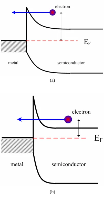
In semiconductor physics, the thermionic-field emission and field emission are both important mechanisms for the transport of electrons over the potential barrier between the metal and the semiconductor. In Schottky barriers on highly-doped silicon crystal as shown in Fig. 1.11(a), the depletion region is so narrow that the electrons can tunnel through the barrier near the top where the barrier is small enough which is called thermionic-field emission. On the other hand, in a degenerate silicon
crystal as shown in Fig. 1.11(b), the electrons can tunnel through the energy barrier even near the Fermi level which is called field emission. It can be found that the tunneling in thermionic-field emission process requires electrons with higher energy than in field emission process. The emission of electrons from a surface of conductive material such as metal or semiconductor into a vacuum environment at an extremely high electric field is also a quantum mechanical tunneling phenomenon. The energy diagram of a metal-vacuum system without external electric field is displayed in Fig. 1.12(a). As shown in Fig. 1.12(b), the vacuum level is bent at extremely high electric field and the energy barrier between the surface of metal and the vacuum become so narrow that the electron can tunnel through it easily, even at very low temperature. Here W0 is the energy difference between an electron at rest outside the metal and an
electron at rest inside the metal, whereas WF is the energy difference between the
Fermi level and the bottom of conduction band. The work function Ф defined as Ф = W0- WF. When a external electric field is applied, the vacuum level is reduced and the
energy barrier at the surface of conductive metal or semiconductor becomes thinner. Then an electron having energy “W” has a finite probability of tunneling through the surface barrier. Fowler and Nordhiem derive the famous Fowler-Noedhiem equation (1.1) as below[1.64-1.65]:
( )
( )
⎥⎥⎦ ⎤ ⎢ ⎢ ⎣ ⎡− = E y v b y t aE J 2 3 2 2 exp φ φ , (1.1)where J is the current density (A/cm2), E is the applied electric field (V/cm), Φ is the work function (eV), a = 1.56×10⁻⁶, b = -6.831×10⁻⁷, y = 3.7947×10⁻⁴E1/2/Ф, t2(y)≒1.1 and v(y) can be approximated as [1.66]. Here
(
y)
y v( )=cos 0.5π (1.2) or 2 95 . 0 ) (y y v = − . (1.3)Typically, the field emission current is measured as a function of the applied voltage V. Substituting relationships of J = I/α and E = βV into Eq. 1.1, where α is the emitting area and β is the local field enhance factor at the emitting surface, following equation can be obtained ⎥ ⎥ ⎦ ⎤ ⎢ ⎢ ⎣ ⎡− = V y bv y t V A I β φ φ αβ 32 2 2 2 ( ) exp ) ( . (1.4)
Then take the log. Form of Eq. 1.4
⎟ ⎟ ⎠ ⎞ ⎜ ⎜ ⎝ ⎛ × − ⎥ ⎦ ⎤ ⎢ ⎣ ⎡ × = ⎟ ⎠ ⎞ ⎜ ⎝ ⎛ − V y v y t V I β φ φ αβ ( ) 10 97 . 2 ) ( 10 54 . 1 log log 2 3 7 2 2 6 , (1.5)
from Eq. 1.5, the slope of a Fowler-Nordhiem (F-N) plot is given by ) ( 10 97 . 2 2 3 7 β φ × = ≡slopeFN S . (1.6)
The parameter β can be evaluated from the slope S of the measured F-N plot if the work function Ф is known,
) ( 10 97 . 2 2 3 7 S φ β ≅− × . (1.7)
Emission area α can be subsequently extracted from a rearrangement of Eq. 1.5
⎟ ⎟ ⎠ ⎞ ⎜ ⎜ ⎝ ⎛ × ⎟ ⎟ ⎠ ⎞ ⎜ ⎜ ⎝ ⎛ = × ⎟ ⎠ ⎞ ⎜ ⎝ ⎛ = − V V I β φ φ β φ α 2 3 7 2 6 2 10 53 . 6 exp 89 . 9 exp 10 4 . 1 . (1.8)
For example, electric field at the surface of a spherical emitter of radius r concentric with a spherical anode (or gate) of radius (r + d) can be represented analytically by ⎟ ⎠ ⎞ ⎜ ⎝ ⎛ + = d d r r V E . (1.9)
Though a realistic electric field in the emitter tip is more complicated than the equation above, we can multiple Eq. 1.9 by a geometric factor β’ to approximate the
real condition. ⎟ ⎠ ⎞ ⎜ ⎝ ⎛ + = = d d r r V d r F Etip ( , ) β' , (1.10)
where r is the tip radius of emitter, d is the emitter-anode(gate) distance, β’ is a geometric correction factor[1.66], and F(r,d) is a function of r and d.
For a very sharp conical emitter tip, where d>>r, Etip approached to β’(V/r).
Moreover, for r>>d, Etip approaches to β’(V/d) which is the solution for parallel-plate
capacitor and for a diode operation in a small anode-to-cathode spacing.
As the tip radius of the gated field-emission array is very small, Eq. 1.10 can be approximated as: ) ( ' r V Etip =β . (1.11)
Combining E=βV and Eq. 1.11, we can obtain the relationship:
) ( ' r V V Etip =β =β and β'=βr, (1.12)
the tip radius r is usually in the range from a few nm to 50 nm, corresponding to the parameter β’ ranging from 10-1 to 10-2.
Besides, transconductance gm of a field emission device is defined as the change
in anode current due to a change in gate voltage[1.67].
ve m Vg Ic g ∂ ∂ = . (1.13)
Transconductance of a field-emission device is a figure of merit that gives as an indication of the amount of current charge that can be accomplished by a given change in gate voltage. The transconductance can be increased by using multiple tips or by decreasing the cathode-to-gate spacing for a given cathode-to-anode spacing.
Since the first observation of CNTs in 1991 by Iijima[1.68], a great deal of attention has been attracted from many researchers due to its unique chemical and physical properties. Due to high aspect ratio, relative low work function, strong mechanical strength, inert chemical properties, good thermal conductivity, and good conductivity, the CNTs are recognized as a wonderful material of electron emitters in field-emission devices. The CNTs were observed as a by-product in the production of the fullerenes by utilizing the arc-discharge method. So far, it can be prepared by several kinds of methods including arc-discharge[1.45], laser ablation[1.69-1.72], and catalytic decomposition of hydrocarbon[1.73-1.80]. Here we make a brief introduction for the methods of CNTs synthesis.
1.3.1 Arc discharge
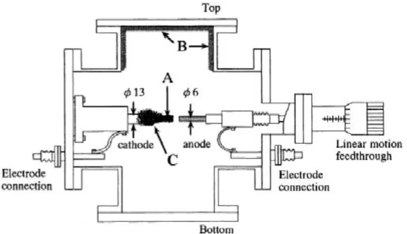
By keeping the gap between the carbon electrodes about 1 mm in the arc-discharge system, CNTs deposits on the surface of the cathode under the conditions that the diameter of the anode carbon is about 8 mm with arc-electric current of 80 A, voltage of 23.5 V, and He pressure of 300 Torr. The CNTs grow only inside the cathode deposit and not exist in other places in the reactor. The quality of CNTs depends on the pressure of He in the reactor and it is also the most important parameter. The optimized pressure of He is about 500 Torr and almost no CNTs are synthesized if the He pressure is below 100 Torr. Another important factor is the electric current for discharge which should be controlled well to keep the arc discharge stable and the electrode cool. The CNTs synthesized by using arc discharge are usually in bundles and need to be released by ultrasonic cleaner and particular etching solution. The arc discharge system is displayed in Fig. 1.13 schematically.
1.3.2 Laser Ablation
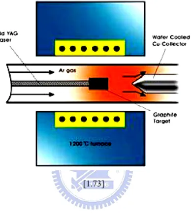
A pulsed or continue laser is applied to vaporize a graphite target in a chamber in He or Ar at about 500 Torr. As the vaporized graphite cooled rapidly, small carbon molecules or atoms condense quickly to form large clusters and then react with the catalyst to form CNTs. Laser ablation is very similar to arc discharge, because the optimum gas pressure and catalyst mix is close to those in the arc discharge process. This might be resulting from very similar reaction conditions required, and the reactions probably occur with the same mechanism. The structure of laser ablation system for synthesizing CNTs is displayed in Fig. 1.14 schematically.
1.3.3 Chemical Vapor Deposition
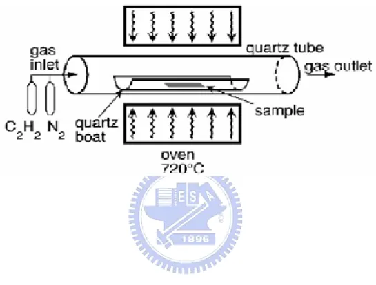
The process of synthesizing CNTs in chemical vapor deposition system includes heating a catalytic material at high temperature and flowing hydrocarbon gas through the reacting chamber for a period of time. The major parameters in the process are hydrocarbon, catalyst, and temperature. Additionally, the plasma enhanced-CVD was also applied to synthesis the CNTs at relative low temperature[1.82-1.83]. The active catalyst species are typically nanoparticles of transition-metal such as Fe, Ni, or Co. The general growth mechanism of CNTs in chemical vapor deposition system involves dissociation of hydrocarbon molecules catalyzed by the transition-metal, and dissolution and saturation of carbon atoms in the nanoparticles. After that, the carbon atoms precipitate from the saturated nanoparticles and form tubular carbon solids in sp2 bonding. Due to containing no dangling bonds, tubule formation has lower formation energy and is favored over other forms of carbon such as graphite sheet with open edges. Moreover, the transition-metals, iron, nickel, and cobalt, are also catalyst used in laser ablation and arc discharge. It may hint that the growth
mechanisms of these three different methods are very similar although different approaches are used to provide carbon feedstock. The structure of the chemical vapor deposition system for synthesizing CNTs is shown in Fig. 1.15.
Generally, the CNTs synthesized by utilizing arc discharge and laser ablation feature with better crystallinity as compared with those synthesized by chemical vapor deposition. However, both the arc discharge and the laser ablation require high temperature processes that make it not possible to grow CNTs-based emitters on glass substrates. Moreover, the arc discharge and laser ablation methods also have the drawbacks of needing more expensive equipments and low throughput. Therefore, the method of synthesizing CNTs by chemical vapor deposition is more attractive for the applications of field-emission displays or back-light units. To make the experiments simpler without complex variables, the thermal-CVD is utilized in our experiments to synthesize the CNTs.
1.4
Motivation
Many relative researches for the synthesis or the field-emission characteristics improvements of the CNTs-based field-emission devices have been reported so far. However, only few of them discussed the problems of reliability and uniformity in the field-emission devices. For the purpose of applications, the issues of reliability and uniformity are two of the most critical keys for the commercialization of field-emission displays and back-light units. Therefore, we focus on the issues of reliability and uniformity of the CNTs-based field-emission devices. Furthermore, the increase of emission current density and power efficiency of the CNTs-based field-emission devices are also discussed here (in Chapter 2 and Chapter 5).
1.4.1 Reliability
Generally, two main problems of reliability for the CNTs-based field-emission devices are observed, an abrupt decrease in emission current with increasing applied electric field[1.84] and a gradual degradation of emission current for a long operating time[1.85-1.88]. These two different phenomena might result from different destruction induced from the applied electric field or the field emission current. As a speculation, the electrostatic force and the Joule heat generated by high current density might be the major factors that degrade the reliability of the field-emission devices. In Chapter 2 and Chapter 3, two novel methods are proposed to improve the contact properties, adhesion and contact resistance, between the CNTs and the substrates to suppress the abrupt decrease and gradual degradation of the emission current in the CNTs-based field-emission devices.
1.4.2 Uniformity
Uniformity is the most difficult challenge for the applications of field-emission displays and back-light units, especially for the displays with image size. Several factors could affect the length of CNTs, such as the thickness of catalyst film, the power of plasma, or distribution of hydrocarbon concentration[1.89-1.90]. Due to the difficulty of controlling the diameter, length, direction, and distribution of the CNTs, it is still hard to obtain a uniform emission current from the CNTs-based field-emission devices. Several methods have been proposed to improve the uniformity of the CNTs-based field-emission devices, such as post plasma treatment, modified catalyst, surface treatment, post laser treatment, critical biasing, and post particle blasting[1-91-1.96]. Part of them could improve the uniformity of the CNTs-based field-emission device, however, some of them had problems of complex
processes, causing defects to the CNTs, or increasing the cost. In Chapter 3, a novel method for the deposition of the catalytic metal layer is utilized to obtain CNTs with uniform morphologies. In Chapter 4, man-made emitters are defined by lithography to control the morphologies and distribution of the emitters precisely.
The main idea in this dissertation is to fabricate CNTs-based field-emission devices with reliable and uniform emission current. To achieve the targets here, additional processes or pretreatments before the growth of CNTs are preferred to avoid the damages caused by some post-treatments. Two novel methods of preparing the catalytic metal layer are proposed to improve the reliability and uniformity of the CNTs-based field-emission devices without generating defects in the CNTs seriously.
1.5
Outline of Dissertation
In the first chapter, the relative backgrounds of this dissertation are introduced briefly including the vacuum microelectronics, the field emission theory, and the technologies of field-emission devices. Here the motivation and main ideas for the design of our experiments are also described simply.
In Chapter 2, the mechanism for the destructions of CNTs in field-emission devices during the field-emission measurements are described according to the measurement data and the material analysis results. A method of thin Ti capping layer on the hydrogen pretreated nanoparticles is also proposed for better reliability. Moreover, this method is also applied to control the CNTs density for increasing the emission current density.
In Chapter 3, a Fe-Ti codeposited metal layer is utilized as the catalyst of the CNTs. For reliability issue, a partially immersed structure is achieved and therefore