ESD Protection Design for 60-GHz LNA With
Inductor-Triggered SCR in 65-nm CMOS Process
Chun-Yu Lin, Member, IEEE, Li-Wei Chu, Student Member, IEEE, and Ming-Dou Ker, Fellow, IEEE
Abstract—To effectively protect the radio-frequency (RF)
cir-cuits in nanoscale CMOS technology from electrostatic discharge (ESD) damages, the silicon-controlled rectifier (SCR) devices have been used as main on-chip ESD protection devices due to their high ESD robustness and low parasitic capacitance. In this paper, an SCR device assisted with an inductor is proposed to improve the turn-on efficiency for ESD protection. Besides, the inductor can be also designed to resonate with the parasitic capacitance of the SCR device at the selected frequency band for RF performance fine tuning. Experimental results of the ESD protection design with inductor-triggered SCR in a nanoscale CMOS process have been successfully verified at 60-GHz frequency. The ESD protection de-sign with inductor-triggered SCR has been implemented in cell configuration with compact size, which can be directly used in the RF receiver circuits. To verify the RF characteristics and ESD ro-bustness in the RF receiver, the inductor-triggered SCR has been applied to a 60-GHz low-noise amplifier (LNA). Verified in a sil-icon chip, the 60-GHz LNA with the inductor-triggered SCR can achieve good RF performances and high ESD robustness.
Index Terms—Electrostatic discharge (ESD), low-noise amplifier
(LNA), silicon-controlled rectifier (SCR), 60 GHz.
I. INTRODUCTION
T
HE 60-GHz frequency band has been allocated for unlicensed usage in the next-generation wireless commu-nications [1]. The radio-frequency (RF) circuits operating at this 60-GHz frequency have the benefits of excellent interference immunity, high security, multi-gigabit speed, and frequency re-usable, due to short transmission distance [2]. Several RF transceivers operated at this frequency had been realized in CMOS technologies [3], [4]. Nanoscale CMOS technologies have been used to implement RF circuits with the advantages of scaling-down feature size, improving high-frequency char-acteristics, low power consumption, high integration capability, and low cost for mass production. However, the thinner gate oxide in nanoscale CMOS technology seriously degrades the electrostatic discharge (ESD) robustness of IC products [5]. The general requirement for a commercial IC product is to pass Manuscript received May 24, 2011; revised November 20, 2011; accepted November 27, 2011. Date of publication January 12, 2012; date of current version March 02, 2012. This work was supported by Taiwan Semiconductor Manufacturing Company (TSMC), by National Science Council, Taiwan, under Contract NSC 100-2221-E-009-048, and by the “Aim for the Top University Plan” of National Chiao-Tung University and Ministry of Education, Taiwan.C.-Y. Lin and M.-D. Ker are with the Institute of Electronics, National Chiao-Tung University, Hsinchu, Taiwan (e-mail: [email protected]; [email protected]). L.-W. Chu is with the Department of Photonics and Display Institute, Na-tional Chiao-Tung University, Hsinchu, Taiwan.
Color versions of one or more of the figures in this paper are available online at http://ieeexplore.ieee.org.
Digital Object Identifier 10.1109/TMTT.2011.2178425
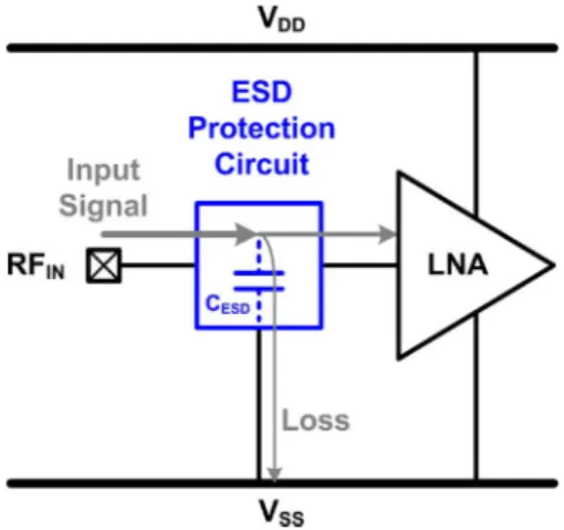
Fig. 1. ESD protection circuit added to the input pad of LNA against ESD damages.
2-kV human-body-model (HBM) ESD tests [6]. Therefore, an on-chip ESD protection circuit must be added at the first stage of the RF receiver. As shown in Fig. 1, the ESD protection cir-cuit is added to the input pad of the low-noise amplifier (LNA) against ESD damages. Several ESD protection designs have been reported for RF circuits [7], [8]. Some ESD protec-tion designs used for 60-GHz RF LNA were also presented [9]–[12]. To minimize the impacts from the ESD protection circuit on RF performances, the ESD protection circuit at the input pads must be carefully designed.
ESD protection devices cause RF performance degradation with several undesired effects [13], [14]. The parasitic capaci-tance of the ESD protection device is one of the most important design considerations for RF circuits. Conventional ESD protection devices with large dimensions have large par-asitic capacitances, which are difficult to be well tolerated in the RF front-end circuits. The parasitic capacitance will cause signal loss from the pad to ground. Moreover, the parasitic ca-pacitance will change the input matching condition. Besides, adding an ESD protection device to the RF receiver will degrade the noise figure. As the operating frequencies of RF circuits are further increased, on-chip ESD protection designs for RF appli-cations are more challenging.
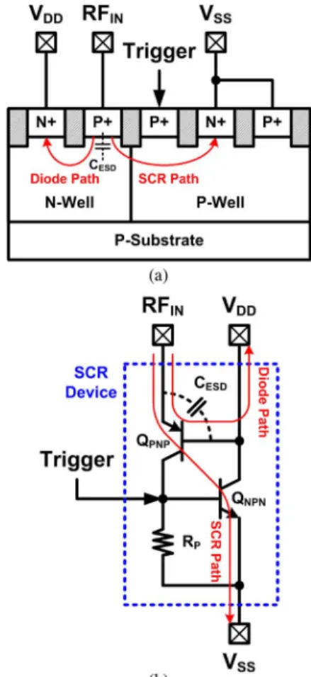
Among the ESD protection devices, such as the diode, MOS, BJT, or field-oxide device, the silicon-controlled rectifier (SCR) device has been reported to be useful for RF ESD protection de-sign due to its higher ESD robustness within a smaller layout area and lower parasitic capacitance [15]. Besides, the SCR de-vice can be safely used without latchup danger in advanced CMOS technologies with low supply voltage [16]. The device structure of the SCR device used in RF input pad is illustrated 0018-9480/$26.00 © 2012 IEEE
in Fig. 2(a). The pad is connected to the first P+, which is formed in the N-well. The pad is connected to the pickup N+, which is formed in the same N-well. The pad is con-nected to the second N+ and the pickup P+, which are formed in the nearby P-well. The trigger port is connected to the third P+, which is formed in the same P-well. The SCR path between and consists of P+, N-well, P-well, and N+. Besides, the parasitic diode path between and consists of P+ and N-well/N+. The equivalent circuit of the SCR consists of
a PNP BJT and an NPN BJT , as shown in
Fig. 2(b). The is formed by the P+, N-well, and P-well, and the is formed by the N-well, P-well, and N+. As ESD zapping from to , the positive-feedback regen-erative mechanism of and results in the SCR de-vice highly conductive to make SCR very robust against ESD stresses. Under RF circuit operating conditions, the diode and SCR paths remain off to prevent from leakage. However, SCR has some drawbacks, such as higher trigger voltage and slower turn-on speed. To reduce the trigger voltage of an SCR device, the trigger signal can be sent into the base terminal of to enhance the turn-on speed. The voltage level of the trigger port is in reverse proportion to the trigger voltage of the SCR device. Therefore, some circuit design techniques are reported to enhance the turn-on efficiency of SCR devices, such as the gate-coupled, substrate-triggered, and gate-grounded-NMOS-triggered (GGNMOS-gate-grounded-NMOS-triggered) techniques [16]. Besides, some SCR devices with lower trigger voltage for RF applications are also presented, such as the diode-triggered SCR (DTSCR) [17]. However, adding a trigger circuit to SCR device also increases the parasitic capacitance seen at the pad, which is hard to tolerate for RF circuits, especially in the 60-GHz operating frequency.
In this work, a novel inductor-triggered SCR design is pro-posed for effective on-chip RF ESD protection for 60-GHz fre-quency. The inductor acts as a conductive path to trigger the SCR device under ESD stress conditions. Besides, the inductor is used to compensate the parasitic capacitance of ESD protec-tion device under normal RF circuit operating condiprotec-tions [18], [19]. This design can achieve low trigger voltage, fast turn-on speed, high ESD robustness, and low RF performance degrada-tion. Without additional process modification, this inductor-trig-gered SCR design is realized by circuit and layout skills in a 65-nm CMOS process.
II. REALIZATION OFINDUCTOR-TRIGGEREDSCR
A. Implementation of the Inductor-Triggered SCR
The new proposed inductor-triggered SCR is shown in Fig. 3, which consists of an SCR device, an inductor , a MOS transistor , and the RC-based ESD detection circuit. The PMOS transistor is selected for since it exhibits the ini-tial-on function for ESD protection, which can quickly pass the trigger signal to SCR device [20]. The inductor is used to pro-vide the trigger path between the pad and the trigger port of the SCR device under ESD stress conditions. The PMOS tran-sistor at the trigger path, which is controlled by the ESD detec-tion circuit, is also turned on under ESD stress condidetec-tions. When the trigger signal passes from the pad to the trigger port
Fig. 2. (a) Device cross-sectional view, and (b) equivalent circuit, of SCR de-vice used in RF input pad.
Fig. 3. Proposed inductor-triggered SCR for RF ESD protection.
of the SCR device, the SCR device can be quickly turned on to discharge the ESD current. The RC-based ESD detection circuit is used to distinguish the ESD-stress conditions from the normal circuit operating conditions. Therefore, under normal power-on conditions, the PMOS transistor is turned off to block the steady leakage current path from the pad to the trigger port of SCR device. Under normal RF circuit operating conditions, the inductor in series with the PMOS is used to compensate the par-asitic capacitance of the SCR device .
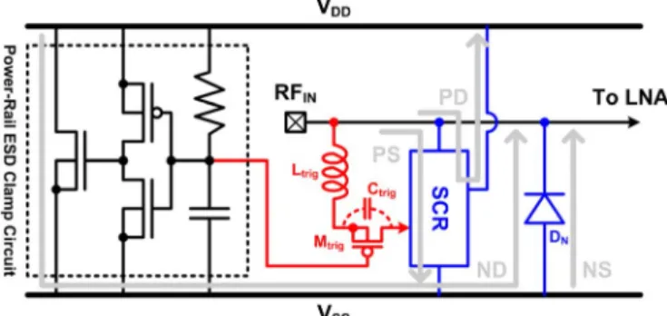
Fig. 4 shows the proposed ESD protection scheme for an RF receiver, including the inductor-triggered SCR, the diode , and the power-rail ESD clamp circuit. The inductor-triggered
Fig. 4. Proposed ESD protection scheme for pad with inductor-triggered SCR, , and power-rail ESD clamp circuit.
SCR assisted with the diode and the power-rail ESD clamp circuit is used to provide the ESD current discharging paths for the pad. The power-rail ESD clamp circuit, which consists of the RC-inverter-triggered NMOS, is used to provide ESD current paths between and under ESD stress conditions. The R ( ) and C ( 10 pF) with the time constant of can distinguish the ESD transients from the normal circuit operating conditions. Under normal circuit operating conditions, the node between R and C is charged to the high potential . Under ESD stress conditions, the ESD voltage at has the fast rise time in the order of 10 ns. With the RC delay, the power-rail ESD clamp circuit is turned on to provide ESD current path from to . Since the power-rail ESD clamp circuit is placed between and , the impact on pad is minor. The RC used in the power-rail ESD clamp circuit can also be used to control the PMOS in the inductor-triggered SCR. With such a configuration, the resistor for ESD detection circuit in the original inductor-triggered SCR can be merged into the power-rail ESD clamp circuit.
In the ESD protection design with the inductor-triggered SCR, the dimensions of the inductor , PMOS transistor , SCR device, and diode can be designed to mini-mize the RF performance degradation. Since the capacitor used in power-rail ESD clamp circuit is large enough ( 10 pF) to keep the node between R and C at ac ground under normal RF circuit operating conditions, the impedance of the trigger path
seen at the pad to ground can be calculated as (1) where the is the angular frequency and the can be ex-pressed as
(2) The , , and denote the gate-to-source capacitance, gate-to-body capacitance, and drain-to-body capacitance of the PMOS transistor , respectively. The resonance angular frequency , which is designed to be the operating frequency of RF signal, can be obtained by
(3)
where the is the parasitic capacitance contributed by the SCR and diode . The sizes of SCR and depend on the required ESD robustness, while the size of transistor de-pends on the required trigger current. Once the sizes of transistor, SCR, and have been chosen, the required induc-tance can be determined.
Fig. 4 also shows the ESD current paths under posi-tive-to- (PS), positive-to- (PD), negative-to-(NS), and negative-to- (ND) ESD stress conditions. During positive-to- ESD stress, ESD current will first pass through the inductor and PMOS to trigger the SCR device. The major ESD current will be discharged by the SCR device from the pad to . Under positive-to-ESD stress, the positive-to-ESD current will be discharged by the parasitic diode path embedded in the SCR device from the pad to . During negative-to- ESD stress, the ESD current will be discharged by the forward-biased from the to pad. Under negative-to- ESD stress, the ESD current will be discharged by the power-rail ESD clamp circuit and the from to pad. The proposed ESD protection scheme in Fig. 4 can provide the corresponding current discharging paths with good ESD robustness.
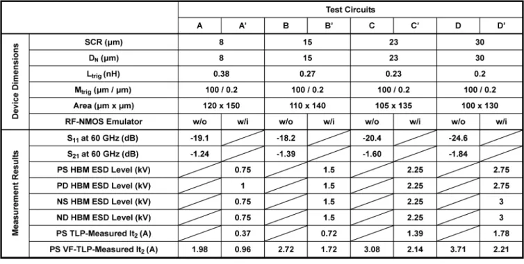
The device dimensions of the test circuits with the inductor-triggered SCR are listed in Table I. A commercial 65-nm CMOS technology is used in this work. The ESD protection circuit with the inductor-triggered SCR is designed for 60-GHz RF applica-tions. The test patterns include the test circuits A, B, C, and D. The size of SCR device used in the test circuits A, B, C, and D are split as 8 , 15 , 23 , and 30 , respectively. The size of in test circuits A, B, C, and D are split as also 8 , 15 , 23 , and 30 , respectively. The parasitic capac-itance of ESD protection devices in test circuits A, B, C, and D at 60 GHz are estimated as 25 fF, 50 fF, 75 fF, and 100 fF, respectively. The width/length of PMOS in each test circuit is kept at , and the equiva-lent is 50 fF at 60 GHz. Therefore, the required inductors , including the parasitic inductance of metal connections, are 0.38 nH, 0.27 nH, 0.23 nH, and 0.2 nH for the test circuits A, B, C, and D.
B. Simulation Under 60-GHz Frequency
The RF characteristics of the test circuits are simulated by using the microwave circuit simulator ADS with the selected device dimensions. Since the SCR model is not provided in the given CMOS process, diodes with P+/N-well, N+/P-well, and N-well/P-well junctions are used to simulate the SCR devices. A signal source with 50- impedance drives the port 1 ( pad) of the test circuit, and a 50- load is connected to the port 2 to simulate the RF receiver. The voltage supply of is 1 V (0 V), and the dc bias of is 0.5 V. The simulated reflec-tion parameters are shown in Fig. 5(a). These ESD protec-tion circuits exhibit good input matching
around 60 GHz. The transmission parameters are compared in Fig. 5(b). At 60-GHz frequency, the test cir-cuits A, B, C, and D have about 0.5-dB, 0.8-dB, 1.2-dB, and 1.5-dB power loss, respectively. Although the parasitic capac-itance of the ESD protection devices can be resonated out, the losses are still contributed by the parasitic resistance of the SCR
TABLE I
DEVICEDIMENSIONS ANDMEASUREMENTSRESULTSESD PROTECTIONDESIGNSWITHINDUCTOR-TRIGGERREDSCR
Fig. 5. Simulation results of proposed ESD protection scheme on (a) -pa-rameter and (b) -parameter.
and . Since these test circuits exhibit good RF performances between 57 65 GHz, they can be operated at 60 GHz even if some variation happens on device values.
C. Simulation Under Normal Power-On Conditions
The test circuits under normal power-on conditions and ESD transient events are simulated by using HSPICE. Under the normal power-on condition, the dc bias of is raised from 0 V to 1 V with 1-ms rise time. The gate voltage of PMOS is biased at 1 V through the resistor of power-rail ESD clamp circuit, so can be kept off and no trigger signal is generated from the pad to the SCR device. Fig. 6(a) shows the HSPICE-simulated voltage waveforms of the test circuit D under the normal power-on condition. The trigger signal remains at 0 V, so the SCR device is kept in off state.
D. Simulation Under ESD Transient Events
When a positive fast-transient ESD voltage is applied to with grounded, the RC delay in the ESD detection circuit keeps the gate of at a relatively low voltage level compared to the fast rising voltage level at . The can be quickly turned on by the ESD energy to generate the trigger signal into the trigger port of the SCR device. Finally, the SCR device can be fully turned on to discharge ESD current from to . Fig. 6(b) shows the simulated voltage waveforms of the test circuit D under the ESD transition, where a 0-to-5 V voltage pulse with 10-ns rise time is applied to to simulate the fast transient voltage of human-body-model (HBM) ESD event [6]. With the limited voltage height of 5 V in the voltage pulse, the simulation results can check the desired trigger function before the RF circuit breakdown.
Fig. 6(c) shows the simulated voltage waveforms of the test circuit D under the other ESD transition, where a 0-to-5 V voltage pulse with 0.1-ns rise time is applied to to simulate the faster transient voltage of charged-device-model (CDM) ESD event [6]. With the large enough trigger signal,
Fig. 6. HSPICE-simulated results of proposed ESD protection scheme under (a) normal power-on condition, (b) ESD-like transition with 10-ns rise time, and (c) ESD-like transition with 0.1-ns rise time.
the SCR device should be triggered on before RF circuit break-down during ESD stress condition.
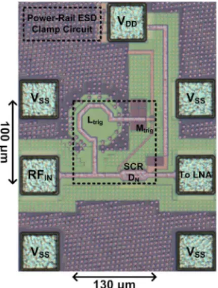
III. EXPERIMENTALRESULTS OFINDUCTOR-TRIGGEREDSCR The test circuits of inductor-triggered SCR have been fabri-cated in a 65-nm salicided CMOS process without using the sili-cide-blocking mask. One set of the test circuits are implemented with ground-signal-ground (G-S-G) pads to facilitate on-wafer two-port S-parameters measurement, which are labeled as test circuits A, B, C, and D. The other set of the test circuits are implemented with the RF-NMOS emulators [12] for ESD tests, which are labeled as test circuits , , , and , as listed in Table I. The RF-NMOS emulator, which consisted of one RF NMOS with gate terminal connected to the pad, and the drain, source, and body terminals connected to pad, is used
Fig. 7. Chip micrograph of test circuit D.
to simulate the RF receiver under ESD stress condition. The ESD robustness of the test circuits can be estimated by the test patterns with the RF-NMOS emulators. Except the RF-NMOS emulator, the device sizes of test circuits A, B, C, and D are equal to those of test circuits , , , and , respectively. The chip micrograph of the test circuit D is shown in Fig. 7.
A. RF Performances
In order to extract the intrinsic characteristics of the test cir-cuits in high frequencies, the parasitic effects of the G-S-G pads have been removed by using the L2L de-embedding technique [21]. With the on-wafer RF measurement, the S-parameters of these four test circuits have been extracted from 0 to 67 GHz. The voltage supply of is 1 V (0 V), and the dc bias of is 0.5 V . The source and load resistances to the test circuits are kept at 50 . The measured -parame-ters and -parameters versus frequencies among the four test circuits are shown in Fig. 8(a) and (b), respectively. As shown in Fig. 8(a), these ESD protection circuits exhibit good input
matching around 60 GHz. At
60-GHz frequency, the test circuits A, B, C, and D have about 1.2-dB, 1.4-dB, 1.6-dB, and 1.8-dB power loss, respectively.
B. ESD Robustness
The human-body-model (HBM) ESD pulses are stressed to each test circuit under positive-to- (PS), positive-to-(PD), negative-to- (NS), and negative-to- (ND) ESD stress conditions. The failure criterion is defined as the I-V char-acteristics seen at shifting over 30% from its original curve after ESD stressed at every ESD test level. In other words, the leakage current under 1-V bias at will not increase over 30% if the test circuit is not failed after ESD stresses. The HBM ESD robustness among the four test circuits with the pro-posed ESD protection designs are listed in Table I. The HBM ESD levels of the proposed ESD protection circuits , , , and can achieve 0.75 kV, 1.5 kV, 2.25 kV, and 2.75 kV, re-spectively, which are obtained from the lowest levels among PS, PD, NS, and ND ESD tests. The HBM ESD robustness of the
Fig. 8. Measurement results of (a) -parameters and (b) -parameters among the four test circuits with the proposed ESD protection scheme under different device dimensions.
test circuits is almost proportional to the sizes of ESD protec-tion devices (SCR and ).
To investigate the turn-on behavior and the I-V characteris-tics in high-current regions of the inductor-triggered SCR, the transmission line pulsing (TLP) system with a 10-ns rise time and a 100-ns pulse width is used [22]. The TLP-measured I-V curves of the ESD protection circuits , , , and under positive-to- stress conditions are shown in Fig. 9. Once ESD pulses stressed to the test circuits, all SCR devices can be quickly triggered on to discharge ESD currents. The secondary breakdown current , which indicated the current-handling ability of ESD protection circuit, can also be obtained from the TLP-measured I-V curve. The test circuits , , , and can achieve of 0.37 A, 0.72 A, 1.39 A, and 1.78 A, respectively. These second breakdown currents measured by TLP system are summarized in Table I. The turn-on behavior and the values of the ESD protection circuits can ensure the effective ESD protection capability of the proposed in-ductor-triggered SCR.
To evaluate the effectiveness of the proposed ESD protection circuits in faster ESD-transient events, another very fast TLP (VF-TLP) system with 0.2-ns rise time and 1-ns pulse width is also used in this study. The VF-TLP system can be used to cap-ture the transient behavior of ESD protection circuits in the time domain of charged-device-model (CDM) ESD event [23]. The VF-TLP-measured of the ESD protection circuits are also listed in Table I. The tests circuits , , , and with the
Fig. 9. TLP-measured I-V characteristics among the four test circuits with the proposed ESD protection scheme of different device dimensions under posi-tive-to- tests.
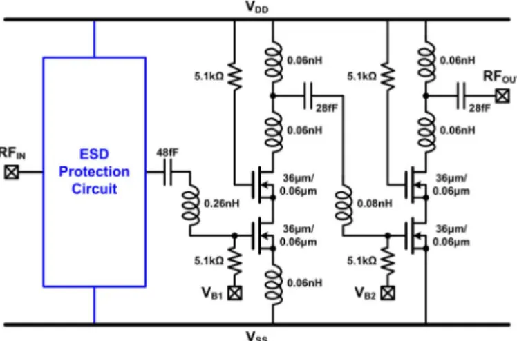
Fig. 10. Circuit schematic of 60-GHz LNA with ESD protection circuit.
RF-NMOS emulator can achieve VF-TLP-measured of 0.96 A, 1.72 A, 2.14 A, and 2.21 A, respectively. For comparison purpose, the tests circuits A, B, C, and D without the RF-NMOS emulator are also tested by VF-TLP system. They can achieve VF-TLP-measured of 1.98 A, 2.72 A, 3.08 A, and 3.71 A, re-spectively. The proposed inductor-triggered SCR is fast enough to be turned on under such a fast-transient pulse.
IV. APPLICATION TO60-GHZLNA
A. 60-GHz LNA Design
One 60-GHz LNA is designed in a commercial 65-nm CMOS technology for verification purpose. The metal-insulator-metal (MIM) capacitors and polysilicon resistors are available in this process.
Fig. 10 shows the schematic of the 60-GHz LNA with ESD protection circuit of inductor-triggered SCR. In the two-stage LNA design, the cascode configuration is utilized to achieve high gain performance. The common-source and common-gate NMOS transistors are all with 36- gate width and 0.06-gate length. The input matching is designed for the minimum noise figure. The output matching network is conjugately matched for the maximum gain.
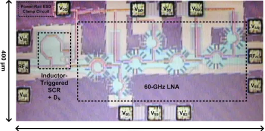
Fig. 11. Chip micrograph of 60-GHz LNA with ESD protection circuit D.
Fig. 12. Measurement results of (a) -parameters and (b) -parameters on 60-GHz LNA with and without ESD protection circuits.
The 60-GHz LNA circuits with ESD protection circuits A and D are included in silicon chip. Fig. 11 shows a chip pho-tograph of the 60-GHz LNA with the ESD protection circuit D. The layout size of this circuit is , including all testing pads and dummy layers. The dummy layers are kept away from the signal paths, so they will not influence the RF signals.
In order to verify the RF characteristics and ESD robustness, the stand-alone LNA without RF ESD protection is also fab-ricated for comparison. All the LNA circuits with and without ESD protection circuits are fabricated on the same wafer for comparison.
B. Experimental Results
The RF characteristics are measured on wafer through G-S-G microwave probes with 100- pitch. The S-parameters are measured by using the Agilent E8361A PNA network analyzer. The short-open-load-thru calibration has been done before the measurements. Each LNA circuit operates with the 1-V supply and draws a total current of 30 mA. The used bias voltages and are all 0.7 V. The measured -pa-rameters and -parameters of the LNA circuits are shown in Fig. 12(a) and (b), respectively. With the ESD protection
circuits, the peak power-gain frequencies of all LNA circuits are at 60 GHz. The input return losses for all test circuits are greater than 10 dB at 60 GHz. The power gains at 60 GHz are 11.1 dB and 10.2 dB for two ESD-protected LNA circuits, respectively, which reduced by 1.1 dB and 2 dB, as compared with the stand-alone LNA of 12.2 dB.
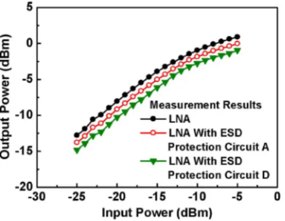
Under the same bias condition, the noise figures and the output power versus input power of the LNA with and without ESD protection circuits are shown in Figs. 13 and 14, re-spectively. The measured noise figures at 60 GHz of two ESD-protected LNA circuits are 7.5 dB and 8.6 dB, respec-tively, and that of the stand-alone LNA is 6.5 dB, as shown in Table II. The input 1-dB compression point of two ESD-protected LNA circuits are 11 dBm, and that of the stand-alone LNA is 12 dBm.
To compare the ESD protection capability among the LNA with and without ESD protection circuits, the RF performances of all LNA circuits after ESD stresses are re-measured. All positive-to- , positive-to- , negative-to- , and neg-ative-to- HBM ESD stresses are zapped to pad of each test circuit. The -parameters of three LNA circuits after various ESD stresses are shown in Fig. 15(a)–(c). The power gain of the stand-alone LNA is severely degraded after 100-V HBM ESD stresses, as seen in Fig. 15(a). In contrast,
TABLE II
COMPARISONAMONG60-GHz LNA WITH ANDWITHOUTESD PROTECTIONDESIGNS INCMOS TECHNOLOGIES
Fig. 13. Measurement results of noise figures on 60-GHz LNA with and without ESD protection circuits.
Fig. 14. Measurement results of output power versus input power on 60-GHz LNA with and without ESD protection circuits.
the power gains of the LNA with ESD protection circuit A and that with ESD protection circuit D are still excellent matching after 500-V and 3-kV HBM ESD stresses, respectively, as seen in Fig. 15(b) and (c).
C. Comparison
Table II summarizes and compares the previously reported 60-GHz ESD-protected LNA [9]–[11] and the circuits of this work. The ESD protection circuit D can provide the required
Fig. 15. Measurement results on -parameters of (a) LNA without ESD pro-tection, (b) LNA with ESD protection circuit A, and (c) LNA with ESD protec-tion circuit D, after PS, PD, NS, and ND HBM ESD stresses.
2-kV HBM ESD robustness with layout area and little RF performance degradation. Moreover, the proposed design has been implemented in cell configuration, which can be directly applied to the 60-GHz RF LNA. Therefore, the pro-posed ESD protection design in this paper is more suitable for RF circuit designer for them to easily apply ESD protection in the 60-GHz RF LNA.
V. CONCLUSION
The new ESD protection scheme with inductor-triggered SCR has been designed, fabricated, and characterized in a 65-nm CMOS process. The inductor-triggered SCR is designed to achieve low trigger voltage and high turn-on speed. More-over, these inductor-triggered SCR can reach the input/output matching with low -parameters and high -parameters. These ESD protection circuits are developed to support RF circuit designers for them to easily apply ESD protection in the 60-GHz RF receiver circuits. Verified in a commercial 65-nm CMOS process, the test circuits A, B, C, and D have about 1.2-dB, 1.4-dB, 1.6-dB, and 1.8-dB power loss at 60-GHz frequency, respectively. Besides, they can sustain 0.75-kV, 1.5-kV, 2.25-kV, and 2.75-kV HBM ESD tests, respectively. The VF-TLP-measured of these test circuits are also provided, which are 0.96 A, 1.72 A, 2.14 A, and 2.21 A, respectively. The test circuits with inductor-triggered SCR have been applied to the 60-GHz LNA to confirm the ESD protection ability and to verify the RF performances. The RF performances of the LNA with ESD protection circuit A and that with ESD protection circuit D are still maintained after 500-V and 3-kV HBM ESD tests are performed, respectively. The inductor-triggered SCR can be further applied to other cir-cuit blocks in the RF transceiver without dc blocking capacitor. Therefore, the proposed ESD protection scheme can be widely used to achieve good RF performance and high ESD robustness simultaneously.
ACKNOWLEDGMENT
The authors would like to thank Mr. T.-H. Lu, Mr. T.-L. Hsu, Mr. P.-F. Hung, Ms. H.-C. Li, Mr. M.-H. Song, Mr. J.-C. Tseng, Mr. T.-H. Chang, Mr. C.-P. Jou, and Mr. M.-H. Tsai of Taiwan Semiconductor Manufacturing Company (TSMC) for their valuable suggestions during RF design and measurement.
REFERENCES
[1] B. Razavi, “A 60-GHz CMOS receiver front-end,” IEEE J. Solid-State
Circuits, vol. 41, no. 1, pp. 17–22, Jan. 2006.
[2] Y. Mimino, K. Nakamura, Y. Hasegawa, Y. Aoki, S. Kuroda, and T. Tokumitsu, “A 60 GHz millimeter-wave MMIC chipset for broad-band wireless access system front-end,” in Proc. IEEE Int. Microwave
Symp., 2002, pp. 1721–1724.
[3] J. Tsai, “A 55–64 GHz fully-integrated sub-harmonic wideband trans-ceiver in 130 nm CMOS process,” IEEE Microw. Wireless Compon.
Lett., vol. 19, no. 11, pp. 758–760, Nov. 2009.
[4] T. Mitomo, R. Fujimoto, N. Ono, R. Tachibana, H. Hoshino, Y. Yoshi-hara, Y. Tsutsumi, and I. Seto, “A 60-GHz CMOS receiver front-end with frequency synthesizer,” IEEE J. Solid-State Circuits, vol. 43, no. 4, pp. 1030–1037, Apr. 2008.
[5] S. Voldman, ESD: RF Technology and Circuits. New York: Wiley, 2006.
[6] M.-D. Ker, J.-J. Peng, and H.-C. Jiang, “ESD test methods on integrated circuits: An overview,” in Proc. IEEE Int. Conf. Electronics, Circuits
and Systems, 2001, pp. 1011–1014.
[7] A. Wang, H. Feng, R. Zhan, H. Xie, G. Chen, Q. Wu, X. Guan, Z. Wang, and C. Zhang, “A review on RF ESD protection design,” IEEE Trans.
Electron Devices, vol. 52, no. 7, pp. 1304–1311, Jul. 2005.
[8] M.-D. Ker, C.-Y. Lin, and Y.-W. Hsiao, “Overview on ESD protection designs of low parasitic capacitance for RF ICs in CMOS technolo-gies,” IEEE Trans. Device Mater. Reliab., vol. 11, no. 2, pp. 207–218, Jun. 2011.
[9] B. Huang, C. Wang, C. Chen, M. Lei, P. Huang, K. Lin, and H. Wang, “Design and analysis for a 60-GHz low-noise amplifier with RF ESD protection,” IEEE Trans. Microw. Theory Tech., vol. 57, no. 2, pp. 298–305, Feb. 2009.
[10] J. Borremans, K. Raczkowski, and P. Wambacq, “A digitally controlled compact 57-to-66 GHz front-end in 45 nm digital CMOS,” in Proc.
IEEE Int. Solid-State Circuits Conf., 2009, pp. 492–493.
[11] S. Thijs, K. Raczkowski, D. Linten, J. Tseng, T. Chang, M. Song, and G. Groeseneken, “CDM protection for millimeter-wave circuits,” in
Proc. EOS/ESD Symp., 2011, pp. 116–122.
[12] C.-Y. Lin, L.-W. Chu, and M.-D. Ker, “Design and implementation of configurable ESD protection cell for 60-GHz RF circuits in a 65-nm CMOS process,” Microelectron. Reliab., vol. 51, no. 8, pp. 1315–1324, Aug. 2011.
[13] K. Gong, H. Feng, R. Zhan, and A. Wang, “A study of parasitic effects of ESD protection on RF ICs,” IEEE Trans. Microw. Theory Tech., vol. 50, no. 1, pp. 393–402, Jan. 2002.
[14] C. Richier, P. Salome, G. Mabboux, I. Zaza, A. Juge, and P. Mortini, “Investigation on different ESD protection strategies devoted to 3.3 V RF applications (2 GHz) in a 0.18 CMOS process,” J.
Electro-statics, vol. 54, no. 1, pp. 55–71, Jan. 2002.
[15] M.-D. Ker and C.-Y. Lin, “Low-capacitance SCR with waffle layout structure for on-chip ESD protection in RF ICs,” IEEE Trans. Microw.
Theory Tech., vol. 56, no. 5, pp. 1286–1294, May 2008.
[16] M.-D. Ker and K.-C. Hsu, “Overview of on-chip electrostatic discharge protection design with SCR-based devices in CMOS integrated cir-cuits,” IEEE Trans. Device Mater. Reliab., vol. 5, no. 2, pp. 235–249, Jun. 2005.
[17] M. Mergens, C. Russ, K. Verhaege, J. Armer, P. Jozwiak, R. Mohn, B. Keppens, and C. Trinh, “Speed optimized diode-triggered SCR (DTSCR) for RF ESD protection of ultra-sensitive IC nodes in ad-vanced technologies,” IEEE Trans. Device Mater. Reliab., vol. 5, no. 3, pp. 532–542, Sep. 2005.
[18] P. Leroux and M. Steyaert, “High-performance 5.2 GHz LNA with on-chip inductor to provide ESD protection,” Electron. Lett., vol. 37, no. 7, pp. 467–469, Mar. 2001.
[19] S. Hyvonen, S. Joshi, and E. Rosenbaum, “Cancellation technique to provide ESD protection for multi-GHz RF inputs,” Electron. Lett., vol. 39, no. 3, pp. 284–286, Feb. 2003.
[20] M.-D. Ker and S.-H. Chen, “Implementation of initial-on ESD pro-tection concept with PMOS-triggered SCR devices in deep-submicron CMOS technology,” IEEE J. Solid-State Circuits, vol. 42, no. 5, pp. 1158–1168, May 2007.
[21] H. Yen, T. Yeh, and S. Liu, “A physical de-embedding method for silicon-based device applications,” PIERS Online, vol. 5, no. 4, pp. 301–305, 2009.
[22] S. Voldman, R. Ashton, J. Barth, D. Bennett, J. Bernier, M. Chaine, J. Daughton, E. Grund, M. Farris, H. Gieser, L. Henry, M. Hopkins, H. Hyatt, M. Natarajan, P. Juliano, T. Maloney, B. McCaffrey, L. Ting, and E. Worley, “Standardization of the transmission line pulse (TLP) methodology for electrostatic discharge (ESD),” in Proc. EOS/ESD
Symp., 2003, pp. 372–381.
[23] C. Chu, A. Gallerano, J. Watt, T. Hoang, T. Tran, D. Chan, W. Wong, J. Barth, and M. Johnson, “Using VFTLP data to design for CDM ro-bustness,” in Proc. EOS/ESD Symp., 2009, pp. 286–291.
Chun-Yu Lin (S’06–M’09) was born in Taiwan in 1984. He received the B.S. degree from the De-partment of Electronics Engineering and the Ph.D. degree from the Institute of Electronics, National Chiao-Tung University, Hsinchu, Taiwan, in 2006 and 2009, respectively.
Since 2009, he has been a Postdoctoral Researcher of the National Chiao-Tung University. His current research interests include ESD protection designs and biomimetic circuit designs. Since 2010, he has also served as the Secretary-General of Taiwan ESD As-sociation.
Li-Wei Chu (S’10) received the B.S. degree from the Department of Electrical Engineering, National Sun Yat-sen University, Kaohsiung, Taiwan, in 2006, and the M.S. degree from the Institute of Electro-Optical Engineering, National Chiao-Tung Univer-sity, Hsinchu, Taiwan, in 2008. Since August 2008, he has been working toward the Ph.D. degree at the Department of Photonics and Display Institute, Na-tional Chiao-Tung University.
His current research interests include the periph-eral circuits integrated on panel for flat panel display applications and the design of 60-GHz ESD protection circuits in CMOS process.
Ming-Dou Ker (S’92–M’94–SM’97–F’08) received the Ph.D. degree from the Institute of Electronics, National Chiao-Tung University, Hsinchu, Taiwan, in 1993.
He worked as the Department Manager with the VLSI Design Division, Computer and Communica-tion Research Laboratories, Industrial Technology Research Institute (ITRI), Hsinchu, Taiwan. Since 2004, he has been a Full Professor with the De-partment of Electronics Engineering, National Chiao-Tung University. During 2008–2011, he
was rotated to be Chair Professor and Vice President of I-Shou University, Kaohsiung, Taiwan. Now, he has been the Distinguished Professor in the Department of Electronics Engineering, National Chiao-Tung University. He served as the Executive Director of National Science and Technology Program on System-on-Chip (NSoC) in Taiwan during 2010–2011; and currently as the Executive Director of National Science and Technology Program on Nano Technology (NPNT) in Taiwan (2011–2014). In the technical field of reliability and quality design for microelectronic circuits and systems, he has published over 450 technical papers in international journals and conferences. He has proposed many solutions to improve the reliability and quality of integrated circuits, which have been granted with 188 U.S. patents and 163 Taiwan patents. He had been invited to teach and/or to consult the reliability and quality design for integrated circuits by hundreds of design houses and semiconductor companies in the worldwide IC industry. His current research interests include reliability and quality design for nanoelectronics and gigascale systems, high-speed and mixed-voltage I/O interface circuits, on-glass circuits for system-on-panel applications, and biomimetic circuits and systems for intelligent prosthesis.
Prof. Ker has served as a member of the Technical Program Committee and the Session Chair of numerous international conferences for many years. He ever served as the Associate Editor for the IEEE TRANSACTIONS ONVERY
LARGE SCALE INTEGRATIONSYSTEMS, 2006–2007. He was selected as the
Distinguished Lecturer in the IEEE Circuits and Systems Society (2006–2007)
and in the IEEE Electron Devices Society (2008–present). He was the President of Foundation in Taiwan ESD Association. In 2009, he was awarded as one of the top ten Distinguished Inventors in Taiwan.