Enhanced spectral response by silicon nitride index matching layer in amorphous
silicon thin-
film solar cells
C.H. Hsu
⁎
, Y.P. Lin, H.J. Hsu, C.C. Tsai
Department of Photonics, National Chiao Tung University, Hsinchu, Taiwana b s t r a c t
a r t i c l e i n f o
Article history:
Received 10 September 2011
Received in revised form 9 December 2011 Available online 9 February 2012 Keywords:
Hydrogenated amorphous silicon thin-film solar cell;
Plasma enhanced chemical vapor deposition; Hydrogenated amorphous silicon nitride
We employed the low temperature hydrogenated amorphous silicon nitride (a-SiNx:H) prepared by plasma-enhanced chemical vapor deposition as a refractive index (n) matching layers in a silicon-based thin-film solar cell between glass (n = 1.5) and the transparent conducting oxide (n = 2). By varying the stoichiometry, refractive index and thickness of the a-SiNx:H layers, we enhanced the spectral response and efficiency of the hydrogenated amorphous silicon thin-film solar cells. The refractive index of a-SiNx:H was reduced from 2.32 to 1.78. Optimizing the a-SiNx:H thickness to 80 nm increased the JSCfrom 8.3 to 9.8 mA/cm2and the corresponding cell efficiency increased from 4.5 to 5.3%, as compared to the cell without the a-SiNx:H index-matching layer on planar substrate. The a-SiNx:H layers with graded refractive indices were effective for enhancing the cell performance.
© 2012 Elsevier B.V. All rights reserved.
1. Introduction
Hydrogenated amorphous silicon (a-Si:H) has received much
atten-tion[1,2]for thin-film solar cell applications due to the following
prop-erties. The bandgap of approximately 1.75 eV makes it suitable for the effective absorption of the solar spectrum. The high absorption coef fi-cient of a-Si:H allows it to absorb light with less material. The low process temperature also realizes the use of low cost glass as substrate, and the material is scalable for large area manufacturing. However, the Staebler–Wronski effect (SWE)[3]induces defects resulting in a decrease in the cell efficiency[4,5]. The degree of degradation due to SWE is related to the material quality and thefilm thickness[6]. The SWE can be reduced by limiting the thickness of a-Si:H absorber, which makes light management more crucial in improving cell efficiency.
The difference in refractive indices causes optical reflection in an electro-optical device. The surface with proper texture can reduce the total reflection which was suggested to be due to the profiled refractive index at the rough interface[7]. Moreover, studies have also reported the improvement of optical reflection by depositing titanium oxide or silicon oxide at the interface between the transparent conduct-ing oxide (TCO) and Si[8,9]. In this work, we employed the low temper-ature hydrogenated amorphous silicon nitride (a-SiNx:H) prepared by
plasma enhanced chemical vapor deposition (PECVD) as a refractive
index-matching (or anti-reflective, AR) layers between glass (n=1.5) and TCO (n = 2). The refractive index of a-SiNx:H can be easily changed
in PECVD through varying the deposition conditions. Moreover, the deposition of a-SiNx:H and the TCOfilms can be carried out at low
temperature. The a-SiNx:H can also act as a passivation layer which
allows the use of low cost substrates containing certain levels of mobile ions. By varying the stoichiometry, refractive index and thickness of the a-SiNx:H layers, the improved cell performance were obtained and
discussed. 2. Experimental
The a-SiNx:Hfilms were deposited on 4 mm glasses by a PECVD
sys-tem at a frequency of 27.12 MHz. It is a commercial load-lock syssys-tem with a maximal substrate size of 20× 20 cm2. Gas mixtures of SiH
4,
NH3and H2 were used and the substrate temperature was kept at
200 °C. The NH3-to-SiH4ratio, rf power and hydrogenflow rate were
varied to obtain different stoichiometry and refractive index of a-SiNx:
H. This a-SiNx:H layer was deposited to have single or graded refractive
index. Then, aflat TCO layer with a thickness of 900 nm was deposited by RF sputtering, followed by a p-i-n a-Si:H solar cell. The a-SiNx:H and
all three layers (p-i-n) were prepared in a single deposition chamber. The thickness of the a-Si:H absorber layer was 300 nm, followed by a TCO/Ag back reflector. The optical reflection was obtained from the UV/VIS/IR spectrometer. The refractive index was measured by an n&k analyzer and was determined at 632.8 nm. The cells had an area of 5 × 5 mm2were patterned for I
–V measurement. The J-V characteristic and the spectral response were measured by an AM1.5 illuminated I–V system and an external quantum efficiency (EQE) measurement, respectively.
Journal of Non-Crystalline Solids 358 (2012) 2324–2326
⁎ Corresponding author.
E-mail address:[email protected](C.H. Hsu).
0022-3093/$– see front matter © 2012 Elsevier B.V. All rights reserved. doi:10.1016/j.jnoncrysol.2011.12.102
Contents lists available atSciVerse ScienceDirect
Journal of Non-Crystalline Solids
j o u r n a l h o m e p a g e : w w w . e l s e v i e r . c o m / l o c a t e / j n o n c r y s o l3. Results
Fig. 1shows the refractive index as a function of the hydrogen
dilution ratio (defined as the H2flow rate divided by the SiH4flow
rate) with different NH3-to-SiH4flow rate ratio (RNH3). The RNH3is
one of the dominant factors which influence the refractive index of a-SiNx:H. Depending on the hydrogen dilution ratio, the refractive
index was reduced approximately from 1.9 to 1.8, with RNH3
in-creased from 5 to 8.3. Moreover, the refractive index was also affected by the hydrogen dilution ratio. Hydrogen is generally introduced to assist the dissociation of reactant gas during deposition. At a smaller RNH3, the introduction of H2 significantly increased the refractive
index. For a larger RNH3, hydrogen still increased the refractive
index slightly. As a result, the minimum refractive index as low as 1.78 was prepared in this study, using RNH3of 8.3 and no additional
hydrogenflow.
Since the refractive index can be changed in-situ by the deposition conditions, the a-SiNx:H with graded refractive index was achieved to
further reduce the optical reflection. Base on the experimental results, thefilms with same thickness had refractive indices of 1.78, 1.86, 1.9, and 1.97 were sequentially deposited on the glass. To investigate the optical characteristics, samples with graded or constant n of the a-SiNx:H AR layers were deposited on 4 mm glasses, followed by a
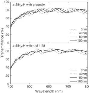
0.9μm-thick TCO. The samples were also confirmed to have negligible roughness by scanning probe microscopy.Fig. 2shows the transmit-tance with different thicknesses of a-SiNx:H AR layers. Due to the
thickness dependent optical interference, the curve of transmittance appears as a periodicfluctuation. With the increasing thicknesses of a-SiNx:Hfilms, the periodic fluctuation of the transmittance shifted
toward long wavelength. The average transmittance of the samples with 80 and 100 nm a-SiNx:H layers was higher than that of the
sam-ples with 0 and 40 nm a-SiNx:H layers in both single or graded case.
The samples with single refractive index showed a smallerfluctuation and a slightly higher transmittance as compared to the samples with graded refractive index.
Fig. 3illustrates the performance of the a-Si:H thin-film solar cells
with different thicknesses of a-SiNx:H having graded refractive index.
The open circuit voltage (VOC) andfill factor (FF) showed no
signifi-cant change when increasing the thickness of a-SiNx:H. In contrast
to the cell without a-SiNx:H, the JSCincreased from 8.3 to 9.8 mA/cm2
and the corresponding efficiency increased from 4.5% to 5.3%. The scat-tering was arising from the experimental error due to the incomplete absorption. The results still indicate a better performance as the thick-ness of a-SiNx:Hfilm was 80 nm.
The external quantum efficiency (QE) of a-Si:H solar cells is shown
inFig. 4. Because there was no front surface texturing in the devices,
the QE in the long-wavelength region fluctuated due to optical
interference. With the addition of a-SiNx:H layers, the shorter
wave-length response slightly increased. As the thickness of the a-SiNx:H
was 40 nm, the QE at wavelengths of 500 and 580 nm had steep decrease. As a result, the current density was even lower than the device without a-SiNx:H. As the thickness was 100 nm, the QE
decreased at the wavelength of 600 nm but increased in the 470–510 nm region. There was an optimized thickness of 80 nm showing a smoother response in the 500–600 nm region. Although there were drops at the wavelengths of 600 and 690 nm, a much
0 70 80 90 100 1.75 1.80 1.85 1.90 NH3/SiH4=8.3 NH3/SiH4=5 1.95
Hydrogen dilution ratio (%)
Refractive index,
n
Fig. 1. Effects of hydrogen dilution ratio and NH3-to-SiH4flow rate ratio on the refrac-tive index of a-SiNx:Hfilm.
400 500 600 700 800 0 20 40 60 80 0 20 40 60 80 100 Wavelength (nm) a-SiNX:H with graded n
a-SiNX:H with n of 1.78
Transmittance (%)
Fig. 2. Transmittance of the samples with different thicknesses of a-SiNx:H AR layer. The upper and lowerfigures show the dependence of graded and single refractive index, respectively. 0 20 40 60 80 100 0.85 0.90 0.95 1.00 7 8 9 10 40 50 60 70 3 4 5 6 VOC (V)
Thickness of a-SiNx:H layer (nm)
JSC
(mA/cm
2)
F.F. ( % )
Efficiency (%)
Fig. 3. J-V characteristics of the cells with different thicknesses of the graded a-SiNx:H layer.
2325 C.H. Hsu et al. / Journal of Non-Crystalline Solids 358 (2012) 2324–2326
better response in the 600–650 nm region resulted in a higher current density of 10.56 mA/cm2.
4. Discussion
The refractive index of glass (n0) is 1.5 and that of TCO (n2) is
ap-proximately 2. According to the equation, n1= (n0n2)1/2, the
theoreti-cally ideal refractive index (n1) of a-SiNx:H as an antireflective layer is
1.73. The refractive index of a-SiNx:H is determined by the
concentra-tion of N in thefilm, which is significantly affected by the deposition conditions. Studies[10,11] have reported the refractive index of a-SiNx:H deposited at low temperature by PECVD can be adjusted
in the range from 1.7 to 2.4. By controlling the power, pressure, and theflow rate ratio of the feeding gas, low refractive indices of a-SiNx:
H can be obtained. As shown inFig. 1, as the RNH3increased, the N
con-tent in a-SiNx:Hfilm increased which resulted in a decreased refractive
index. The addition of H2also affects thefilm content and the resulting
refractive index. The H2may increase the dissociation in the plasma, but
also increase the etching on the surface. The preferential etching of the N–H bonding by the hydrogen plasma was proposed to increase the re-fractive index[12]. As a result, the lower hydrogen dilution ratio would further lowered the refractive index. A minimum refractive index of 1.78 was obtained when there was no hydrogen in the feeding gas.
The glass used in this study had no particular treatment to reduce the iron content. Therefore, the transmittance in the shorter wave-length region was significantly lower (Fig. 2) because of the absorption due to charge transfer process[13]. Although the practical transmit-tance would be affected by the following p-i-n device, this still indicated that the reflection of the devices with AR coating can be minimized at certain particular wavelengths, and could have higher reflection at others. As can be seen inFig. 2, the transmittance of the samples with a-SiNx:H AR layers having n of 1.78 have a similar trend to that of the
samples with a-SiNx:H having graded n. The average transmittance of
the samples with constant n was slightly higher than that with graded n. However, the solar cells consisted of these AR layers showed no significant difference. This may be due to the further influence of the p-i-n device which reduced the small transmittance difference. More-over, the difference of refractive index between glass and TCO may also be too small, so that the refractive index of 1.78 was already effec-tive in improving the cell performance. To further improve the index matching by graded n, materials such as silicon oxide (SiOx) or silicon
oxynitride (SiOxNy) can also be deposited by PECVD. The materials
can have refractive indices as low as approximately 1.5 which is closer to the refractive index of glass.
A same device process carried out on a textured SnO2:F glass can
achieve an efficiency of 9.45% with VOC= 0.91 V, JSC= 14.42 mA/cm2
and FF = 72.36%[14]. In this study, planar substrates were used to investigate the effect of a-SiNx:H index-matching layers. The results
inFig. 3 showed a higher VOC of the device than the one on the
above mentioned textured SnO2:F glass, which may be due to the
less interface recombination from the planar structure. The improve-ment of JSCcontributed by the AR layer was the main factor for
en-hancing the performance of the a-Si:H solar cells. An optimized thickness of 80 nm of the graded a-SiNx:H AR layer was observed
from the J-V characteristics.
The QE measurement also showed an optimized current density as the thickness was 80 nm, which is shown inFig. 4. A relative increase of 2.3% (from 10.32 to 10.56 mA/cm2), as compared to the device without a-SiNx:H on planar substrate was obtained, owing to the
in-creases in the wavelength region of 510–560 nm and 610–660 nm. Considering the standard AM1.5 solar spectrum, a higher irradiance was located in the range from 480 to 600 nm. According to the equa-tion of quarter-wavelength (d =λ/4n), a corresponding ideal thick-ness from 67 to 82 nm was attained for the a-SiNx:H having
refractive index of 1.78. The calculated value was close to the experi-mental result of 80 nm. The disadvantage of the QE in the long wave-length region may be able to be improved through further texturing of the substrates.
5. Conclusions
We were able to deposit the a-SiNx:H layer with refractive index
as low as 1.78 through varying the deposition conditions. By optimizing the thickness and the refractive index of the a-SiNx:H index-matching
layer, we have achieved an enhanced absorption in the range of 500–600 nm, where the solar spectrum has a higher intensity. The results showed improvements of the J-V characteristics, mainly due to the increasing short-circuit current. Compared to the cell without a-SiNx:H layer on non-textured substrate, the cell with 80 nm
a-SiNx:H AR layer increased the JSCfrom 8.3 to 9.8 mA/cm2, and the
corresponding cell efficiency was increased from 4.5 to 5.3%. A rela-tive improvement of 2.3% in current density as measured by QE was also confirmed.
Acknowledgement
This work was supported by the Center for Green Energy Technolo-gy at the National Chiao Tung University, the National Science Technol-ogy Program-Energy of National Science Council and the Nexpower Technology Corporation in Taiwan.
References
[1] B. Rech, H. Wagner, Appl. Phys. A. 69 (1999) 155.
[2] P. Roca i Cabarrocas, Curr. Opin. Solid State Mater. Sci. 6 (2002) 439. [3] D.L. Staebler, C.R. Wronski, Appl. Phys. Lett. 31 (1977) 292. [4] J. Yang, S. Guha, Appl. Phys. Lett. 61 (1992) 2917. [5] M. Ito, M. Kondo, Jpn. J. Appl. Phys. 45 (2006) L230.
[6] R.J. Koval, J. Koh, Z. Lu, L. Jiao, R.W. Collins, C.R. Wronski, Appl. Phys. Lett. 75 (1999) 1553.
[7] J. Springer, A. Poruba, M. Vanecek, J. Appl. Phys. 96 (2004) 5329. [8] T. Fujibayashi, T. Matsui, M. Kondo, Appl. Phys. Lett. 88 (2006) 183508. [9] C. Das, A. Doumit, F. Finger, A. Gordijn, J. Huepkes, J. Kirchhoff, A. Lambertz, T.
Melle, W. Reetz, Sol. Energy Mater. Sol. Cells 93 (2009) 973–975.
[10] T. Lauinger, J. Moschner, A.G. Aberle, R. Hezel, J. Vac. Sci. Technol., A 16 (1998) 530.
[11] T.M. Klein, T.M. Anderson, A.I. Chowdhury, G.N. Parsons, J. Vac. Sci. Technol., A 17 (1999) 108.
[12] Y. Kuo, Appl. Phys. Lett. 63 (1993) 144.
[13] T. Uchino, K. Nakaguchi, Y. Nagashima, T. Kond, J. Non-Cryst. Solids 261 (2000) 72.
[14] P.H. Cheng, S.W. Liang, Y.P. Lin, H.J. Hsu, C.H. Hsu, C.C. Tsai, Mater. Res. Soc. Symp. Proc. 1321 (2011) 39. 300 400 500 600 700 800 0 25 50 75 100 QE (%) Wavelength (nm) 0 10.32 ± 0.2 40 10.26 ± 0.2 80 10.56 ± 0.2 100 10.40 ± 0.2 Current density (mA/cm2) Thickness (nm)
Fig. 4. External quantum efficiency of a-Si:H thin-film solar cells with different thick-nesses of a-SiNx:H layers having graded refractive index.