IEEE ELECTRON DEVICE LETTERS, VOL. 12, NO. 5, MAY 1991 249
Effect
of
Back-Gate Bias on Tunneling
Leakage in a Gated p+-n Diode
Ming-Jer Chen, Member, IEEEAbstract-On a thin-oxide gate-controlled p+-n diode, this work k i t exhibits experimentally not only the substrate-bias-de- pendent charactenstics of the tunneling leakage current but also the tunneling leakage characteristics independent of the sub- strate bias. This observation can be reasonably explained by the nature of the modulation of the surface space-charge region over the heavily doped p+ region as well as over the n-type substrate. Based on this work, the original understanding of such tunneling leakage has been improved.
I. INTRODUCTION
N 1965, Grove and Fitzgerald [l] presented experimen-
I
tally the back-gate bias dependence of the leakage current through a gated p+-n diode whose oxide was intentionally contaminated with sodium ions. For such a diode having a highly doped p+ region, they proposed empirically a tunnel- ing mechanism invoIved in an induced junction formed be- tween an inversion layer over the p+ region and the underly- ing p+ region. Recently, a new tunneling leakage occurring in the gate-to-drain overlap region for scaled-down thin oxide MOSFET's has been extensively studied [2], [3]. Chang and Lien [2] and Chan et d . [3] have shown this leakage current experimentally to be independent of back-gate bias or sub- strate bias. To interpret this relationship, they together pro- posed the deep-depletion approximation theory by not form- ing an inversion layer over the heavily doped region. On a thin-oxide PMOSFET or, equivalently, a thin-oxide gate-con- trolled p+-n diode, however, we will present experimentally a new phenomenon that the previous theories [1]-[3] fail to interpret.II.
EXPERIMENTThe structure under test consists of 864 gated p+-n diodes in parallel. Fig. 1 shows the cross section of one such diode where the simulated potential contours are superimposed and will be discussed later. This structure has been fabricated using the conventional n-well CMOS process. The gate oxide thickness is about 250 %, and the total peripheral length is 124416 pm. The junction depth and surface doping concen- tration of the p+ region are about 0.44 pm and 4 x l O I 9 cmP3, respectively. The temperature measurements have been performed to identify the band-to-band tunneling mechanism responsible for the measured leakage characteristics.
Manuscript received January 28, 1991. This work was supported in part by the National Science Council under Contract NSC 79-0404-E-009-50 and by National Chiao-Tung University.
The author is with the Institute of Electronics, National Chiao-Tung University, Hsin-Chu, Taiwan 30039, Republic of China.
IEEE Log Number 9100090.
Oxide
250 .% 0
Distance (um)
Fig. 1 . Cross section of a gate-controlled p+-n diode. Also shown are the simulated potential contours corresponding to V, = 0 V, V, = 10 V, and
v,,
= 2v.
10.'I
-6OOc'I
1 0 ' ~ -8
lo.lo 10." - 10-12 - n w 10-l) I 0 2 4 6 8 1 0-vD
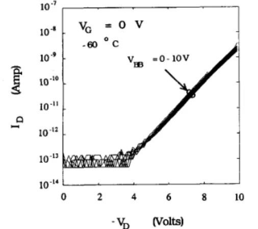
(volts)Fig. 2. Measured leakage characteristics at -60°C with back-gate bias ranged from 0 to 10 V in 1-V steps for all the gates grounded.
At -60°C and with all of the gates grounded, Fig. 2 shows the measurement results of the leakage current ID
versus the drain voltage V, with the back-gate bias VBB as a parameter. From Fig. 2, it can be observed that the leakage current is nearly independent of the back-gate bias. By changing the test condition from the gates grounded to the p+ regions grounded, however, a great difference in the result- ing leakage characteristics occurs. For all of the p+ regions grounded, Fig. 3 shows the measurement results of the leakage current ID versus the gate voltage V, with VBB = 2 0741-3106/91/0500-09$O1.00 0 1991 IEEE
- -
____
~.
250 IEEE ELECTRON DEVICE LETTERS, VOL. 12, NO. 5 , MAY 1991
8
10.~e
,3
t lo-* i 1 0 . ~ 10-l0 VD= o v
-
-18 O C I 0 2 4 6 8 1 0 1 2v,
(Volts)Fig. 3. Measured leakage characteristics at two temperatures of -18 and
-6O'C with two back-gate biases of 2 and 4 V for all the p+ regions grounded.
8
n c( 10 1 0 . ~ 10.10 10'" 10.''shown experimentally both the back-gate bias dependence and the back-gate bias independence of such leakage current. The previous theories [1]-[3] fail to explain this new phe- nomenon and should be considerably improved.
III.
DISCUSSIONTo account for the above experimental results, the two-di- mensional potential distributions in a gated p+-n diode as a function of V, and V,, under V, = 0 V are of concern. Based on the measured doping profile, a two-dimensional device simulator PISCES
II-B
[5] has been utilized to offer the corresponding potential distributions. Fig. 1 shows such potential contours under V, = 10 V, V,, = 2 V, and V, =0 V. From Fig. 1, it can be clearly observed that the surface of the p + region near the comer is inverted. Moreover, the simulation has shown that an increase in V,, can cause a decrease in the regime located by such an inversion layer until the p+ surface is completely depleted. For example, the inversion region in Fig. 1 completely disappears as V,, exceeds about 5 V. Also, the simulation has shown that the corresponding surface electric field strength near the comer increases and then tends to saturation. Based on this simula- tion work, we present the following new mechanism in order to better interpret the experimental results.
According to Fig. 1, for the formation of an inversion layer over the p + surface, the following two conditions must be satisfied simultaneously: and (2) 0 2 4 6 8 10 VG V T , p
v,,
(volts)Fig. 4. Measured leakage current versus back-gate bias at -6O'C with gate voltage as a parameter for all the p+ regions grounded. The gate voltage ranges from 0 to 10 V in 1-v steps.
where VF,,, is the flat-band voltage for the MOS system on the substrate and VT,p is the threshold voltage to induce an inversion layer near the comer over the p+ surface. The voltage VT,p can be expressed as [6]
and 4 V for two differetlt temperatures of -18 and -60°C. The corresponding characteristics of the leakage current ver- sus the back-gate bias at -60°C with the gate voltage as a parameter are shown in Fig. 4. The measured leakage current shown in Fig. 3 exhibits a positive temperature coefficient, i.e., the leakage current increases as the temperature in- creases, indicating the band-to-band tunneling mechanism dominating the measured leakage characteristics in our work. As we increase V, negatively to a large value (-10 V, for example), we have found a negative temperature coefficient of not only the drain leakage current occurring in the gate-p+ overlap region but also the gate leakage current through the gate-p+ overlap oxide, indicating the dominance of the surface avalanche impact ionization [4]. Note that the ID
versus V, curves for large value of V,, deduced from Fig. 4 are nearly identical to the ID versus -VD curves shown in Fig. 2. We can observe from Fig. 4 that for both small values
of V,, and large values of V, the leakage current is
modulated over a very large range by the application of a back-gate bias; however, as the V,, value increases, the leakage current tends to saturation and thus becomes consid- erably independent of the back-gate bias. Therefore, we have
where V,,,, is the flat-band voltage for the MOS system on the p+ region, to, is the gate oxide thickness, es is the silicon permittivity,
n i
is the effective intrinsic concentration, and NA is the position-dependent surface doping concentra- tion of the diffised p+ region. Note that VT,p is a position- dependent parameter along the surface of the p+ region. Equation (1) reveals the condition for the accumulation layer appearing over the substrate and (2) gives the condition for the formation of an inversion layer over the p+ surface. Note that (2) is valid only when (1) has been satisfied. This is because the accumulation layer itself acts as a conductive path via which the back-gate bias V,, is electrically con- nected to the possibly formed inversion layer over the p+ region. Therefore, any condition (1) or (2) not satisfied will make the tunneling leakage characteristics independent of the back-gate bias.CHEN: EFFECT OF BACK-GATE BIAS ON TUNNELING LEAKAGE IN GATED P+-N DIODE 25 1
The experimental ID versus VD curves shown in Fig. 2
can be interpreted by noting that (1) is not satisfied since the measured value of VF,J = 0.3 V) is greater than ( V,
-
V,,). Depending on the values of VBB and V,, the part of the curves shown in Fig. 4 where the leakage currents are about independent of V,, can be divided into two regimes: the left-side regime, where (1) is satisfied while (2) is not, and the right-side regime, where (1) is not satisfied. Only for the case of s m a l l V,, and large V, values can (1) and (2) be
satisfied simultaneously. Under this condition, the pf surface near the comer is inverted. The formation of such an inver- sion layer provides the path for the back-gate bias to reduce the effective electrical field strength, leading to the back-gate bias dependence mentioned abdve.
IV.
CONCLUSIONThis work has demonstrated that for a thin-oxide gated p+-n diode, not only back-gate bias dependence but also back-gate bias independence of the tunneling leakage current have been observed. The nature of the modulation of the surface space-charge region over each side of the junction has been proposed for this observation.
ACKNOWLEDGMENT
The author would like to thank Dr. N.-S. Tsai and P.-N. Tseng of Taiwan Semiconductor Manufacturing Company for device processing, and S.-J.
Wu
for device measurement. The author would also like to thank T.-H. Huang of National Chiao-Tung University for performing the released PISCESII-B
simulator.REFERENCES
A. S. Grove and D. J. Fitzgerald, “The origin of channel currents associated with p+ regions in silicon,” IEEE Trans. Electron Devices, vol. ED-12, pp. 619-626, 1965.
C. Chang and J. Lien, “Comer-field induced drain leakage in thin oxide MOSFETs,” in IEDM Tech. Dig., 1987, pp. 714-717. T. Y. Chan, J. Chen, P. K. KO, and C. Hu, “The impact of gate-induced drain leakage current on MOSFET scaling,’’ in IEDM Tech. Dig., 1987, pp. 718-721.
M. J. Chen, “New observation of gate current in off-state MOSFET,” to be published.
M. R. Pinto, C. S. RafTerty, and R. W. Dutton, “PISCES-II: Poisson and continuity equation solver,” Stanford Electron. Lab., Stanford, CA, Tech. Rep., Sept. 1984.
R. S. Muller and T. I. Kamins, Device Electronics for Integrated Circuits, 2nd ed. New York: Wiley, 1986, pp. 395-399.