Architecture Design of Shape-Adaptive Discrete
Cosine Transform and Its Inverse
for MPEG-4 Video Coding
Hui-Cheng Hsu, Kun-Bin Lee, Member, IEEE, Nelson Yen-Chung Chang, Student Member, IEEE, and
Tian-Sheuan Chang, Senior Member, IEEE
Abstract—This paper presents efficient VLSI architectures of
the shape-adaptive discrete cosine transform (SA-DCT) and its inverse transform (SA-IDCT) for MPEG-4. Two of the challenges encountered during the exploitation of more efficient architectures for the SA-DCT and SA-IDCT are addressed. One challenge is to handle the architectural irregularity due to the shape-adap-tive nature. The other one is to provide acceptable throughput using minimal hardware. In the algorithm-level optimization, this work exploits the numerical properties found in the trans-form matrices of various lengths, and derives a fine-grained zero-skipping scheme for the IDCT which can perform 22.6% more zero-skipping than the common vector-based coarse-grained zero-skipping scheme does. In the architecture-level design, the 1-D variable-length DCT/IDCT architectures designed on the basis of the numerical properties are proposed. An auto-aligned transpose memory that aligns the data of different lengths is also incorporated. In addition, a zero-index table is also included in the transpose memory to support the fine-grained zero-skipping in the SA-IDCT. The synthesized designs of the SA-DCT and SA-IDCT are implemented using UMC 0.18- m technology. The SA-DCT architecture has 26 635 gates, and its average cycle-throughput is 0.66 pixels/cycle, which is comparable to other proposed architec-tures. On the other hand, the SA-IDCT architecture has 29 960 gates, and its cycle-throughput is 6.42 pixels/cycle. While decoding for CIF@30FPS, the SA-IDCT is clocked at 0.7 MHz, and the power consumption is 0.14 mW. Both the throughput and power consumption of the proposed SA-IDCT architecture are an order better than those of the existing SA-IDCT architectures.
Index Terms—Discrete cosine transform (DCT), MPEG-4, video
coding, VLSI.
I. INTRODUCTION
M
PEG-4 object-based video coding can achieve higher subjective picture quality, increased coding efficiency, as well as better user interactions. Many techniques for coding arbitrarily shaped image segments have been proposed [1]–[3]. Among these techniques, the shape-adaptive discrete cosine transform (SA-DCT) and its inverse transform (SA-IDCT) proposed by Sikora et al. [2] have been adopted in MPEG-4Manuscript received May 8, 2005; revised April 4, 2006 and February 1, 2007. This paper was recommended by Associate Editor S. Panchanathan.
H.-C. Hsu and K.-B. Lee are with MediaTek, Inc., Hsinchu 300, Taiwan, R.O.C.
N. Y.-C. Chang and T.-S. Chang are with National Chiao-Tung University, Hsinchu 300, Taiwan, R.O.C. (e-mail: [email protected]).
Color versions of one or more of the figures in this paper are available online at http://ieeexplore.ieee.org.
Digital Object Identifier 10.1109/TCSVT.2008.918275
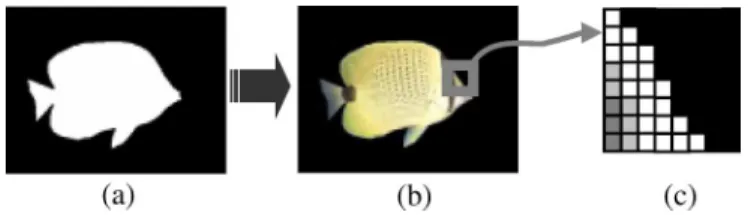
Fig. 1. Relation among (a) shape, (b) texture, and (c) boundary block in a video object.
standard [4]. The SA-DCT/SA-IDCT performs forward/inverse DCT for the pixels within a video object of arbitrary shape, as illustrated in Fig. 1. Instead of performing a full 8 8 DCT after filling zeros to the nonobject pixels, the SA-DCT adap-tively performs -point DCTs based on the shape, where represents the length of rows/columns within the video object in a block. Comparing SA-DCT with the combination of filling and 8 8 DCT, the SA-DCT provides a significantly better rate-distortion tradeoff [5].
However, as the shape of a video object varies, the irregularity of variable-length DCT/IDCT gives challenges to efficient ar-chitecture design. These challenges have not been encountered in the architecture design of traditional 8 8 DCT/IDCT. One of the major challenges is how to efficiently allocate computing resources for the computation of variable-length DCT/IDCT so that the throughput can still be acceptable. Another chal-lenge is to cope with the irregularity due to the consecutive vari-able-length rows or columns computation which would signifi-cantly affect the pipeline schedule and the hardware efficiency. To conquer the aforementioned challenges, we propose a hardware-efficient SA-DCT/IDCT architecture based on algorithm-level and architecture-level optimizations. In the algorithm-level optimization, we first explore the numerical properties within the transform matrices to reduce the computa-tional requirements. Our exploration goes beyond the tradicomputa-tional even/odd symmetry in the 8 8 DCT/IDCT and covers all possible numerical properties in different transform lengths. This enables the proposed architecture to provide throughput comparable to other SA-DCT/IDCT architectures with less computing resource. In addition, we adopt a fine-grained zero-skipping scheme instead of the traditional coarse-grained zero-skipping scheme for the proposed SA-IDCT architec-ture. The proposed fine-grained zero-skipping scheme reduces both the computation and memory access at the same time. 1051-8215/$25.00 © 2008 IEEE
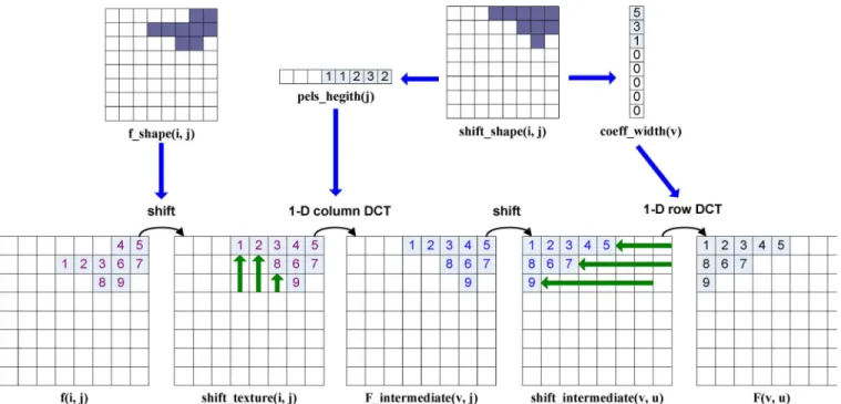
Fig. 2. Process of SA-DCT computation.
Moreover, the fine-grained zero-skipping explores all possible skipping of transform computation on zero-valued inputs.
On the other hand, the architecture-level optimizations include careful scheduling based on the proposed three-stage pipelined architecture, the introduction of an auto-aligned transpose memory, and the use of a zero-index table. The archi-tecture-level scheduling is based on the numerical properties explored during algorithm-level optimization. To handle the irregularity due to the shape-adaptive nature, the auto-aligned transpose memory is introduced to align rows and columns automatically based on the video object’s shape information. In addition, the zero-index table is incorporated to enable the fine-grained zero-skipping scheme for the proposed SA-IDCT architecture. With the above optimizations, the proposed SA-DCT/IDCT architecture represents an efficient solution to overcome the challenges mentioned earlier.
The remainder of this paper is organized as follows. Section II first presents a brief introduction to the operations of the SA-DCT and SA-IDCT. Section III presents the related works on the DCT/IDCT and the SA-DCT/SA-IDCT architectures. The numerical properties exploited in the transform matrices and the fine-grained zero-skipping schemes are explained in Section IV. Section V introduces the proposed architectures of the SA-DCT/SA-IDCT. Design considerations of the archi-tectures are also explained in Section V. Section VI presents the implementation comparison of the SA-DCT/SA-IDCT architectures. Finally, Section VII concludes this work.
II. SA-DCTANDSA-IDCT
The definition of the forward SA-DCT illustrated in Fig. 2 is based on the four subsequent processing steps listed as follows.
S1) Vertically shift all object pixels in to the upper
most position to construct . Also
construct the auxiliary in the same
way.
S2) Apply 1-D variable-length DCT to the
first pels in all columns of
with .
S3) Horizontally shift all intermediate coefficients in to the left most position to
construct .
S4) Apply 1-D variable-length DCT to the first intermediate coefficients in
all rows of with
.
The alignment in the SA-DCT is illustrated in Fig. 2, where the indexes denote the object pixels. The th DCT coefficient
of a 1-D -point DCT on data is
calculated as
(1)
where and for
. For the considered shape-adaptive trans-form, varies for each row and column, which is controlled by a binary array that describes the shape of the input data . This binary array element is collocated with the pixel of the corresponding 8 8 block. An
aux-iliary binary array and two 1-D counter
arrays and are computed
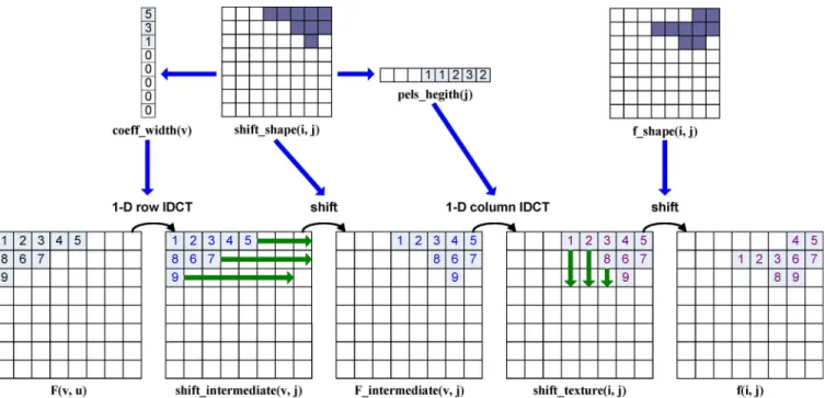
Fig. 3. Process of SA-IDCT computation.
forward SA-DCT to generate the data position and the length of 1-D DCT.
At the inverse side, the process is reversed to recover an image, as shown in Fig. 3. The definition of the SA-IDCT is based on the five subsequent processing steps I-S1)–I-S5).
I-S1) Compute the required shape parameters
, and
from the decoded binary shape array .
I-S2) Apply 1-D variable-length IDCT to the first decoded coefficients in all rows
of with . Store
the reconstructed intermediate coefficients in .
I-S3) Horizontally shift all reconstructed intermediate
coefficients in from
the left most position to their original column
position defined by . Store the
horizontally shifted intermediate coefficients in .
I-S4) Apply 1-D variable-length IDCT to the first intermediate coefficients in
all columns of with
.
I-S5) Vertically shift all reconstructed pixels in
from the upper most position to their original row position defined by . The shift operations of I-S3) and I-S5) are shown in Fig. 3, where the indexes denote the object coefficients. The th data
of an -point 1-D IDCT for coefficient
is calculated as
(2)
where and for
. As in the SA-DCT, varies for each row and column in the SA-IDCT.
III. RELATEDWORK
Previous designs on variable-length DCT and IDCT can be classified into two approaches: variable length in nature design [6], [7] and extension of 8 8 DCT and IDCT [8], [9]. Vari-able length in nature design adopts the recursive algorithm and architecture [6]. Although recursive designs have several advan-tages including modularity and scalability, they have a compu-tational complexity which equals to the worst case of the direct implementation scheme. To tackle the problems of numerical in-stability found in the time-recursive design, Le and Glesner [7] proposed the feedforward architecture. However, they did not address the issues of transposing and shifting the variable-length DCT coefficients during the computation process, which are vital for both the SA-DCT and SA-IDCT.
The extension approaches extend the architectures of fixed 8-point DCT and IDCT to support variable-length DCT/IDCT. Tseng [8] proposed a reconfigurable architecture that can per-form standard 2-D 8 8 DCT/IDCT and 2-D SA-DCT/IDCT. Tseng’s variable-length 1-D DCT/IDCT is based on Madisetti’s design [10] which performs eight regular multiplications, but Tseng’s design performs seven constant multiplications instead. In addition, the shape formation, texture alignment, texture, and shape transpose memories are incorporated into Tseng’s design to complete the 2-D SA-DCT/IDCT. Owzar et al. [9] extends a
standard 8 8 IDCT hardware architecture with the shape pa-rameter extraction by using counting and comparing operations on row indexes and length registers.
As to the low-power DCT/IDCT design, most of the pre-vious approaches explore the property of zero-valued inputs to save power [11]–[16]. Xanthopolous [11] exploits the rela-tive occurrence of zero-valued DCT coefficients coupled with clock gating, which can reduce the power but cannot reduce the required computation time. Pai’s [12] design uses Loeffler’s [17] fast algorithm to reduce the multiplications and uses zero bypassing, data segmentation, input truncation, and hardwired canonical sign-digit (CSD) multipliers to reduce the run-time computation requirement. However, Pai’s zero bypassing is per-formed mainly by data gating and did not reduce the computa-tion cycles.
Being aware of the need to further reduce the computation cy-cles, Bae and Min [13] uses the sparsity of the IDCT input coef-ficients to compute only non-zero valued coefcoef-ficients, which is different from Pai’s approach. According to the simulation re-sults, their algorithm is faster than the conventional algorithms by a factor of 2 to 10. Although Bae’s algorithm speeds up the computation efficiently, their architecture can not reduce the memory access. Besides, they did not describe how the non-zero input is fed into the IDCT.
Lin [14] proposes an alternative high-performance Inverse-Scan DCT (ISDCT) architecture, which not only skips the com-putation of zero-value coefficients, but also merges the functions of inverse scan and IDCT without an additional inverse scan buffer. However, since Lin’s ISDCT processes the data in the zigzag scan order instead of the common raster scan order, every intermediate partial product has to be stored in the memory and retrieved again for accumulation, which will increase the power consumption.
Chen et al. [18]–[20] propose an adder-based DCT/IDCT de-sign which can adjust the coefficient’s precision adaptively to achieve power reduction. Their IDCT engine is later adopted in [15]. In addition to adaptive precision adjustment, [15] also adopted the zero-vector detection technique to skip the trans-form computations for zero-vector inputs. Though the compu-tation for the zero-vector is reduced in [15], the memory ac-cess is not reduced. In [16], both the computation and memory access are reduced at the same time by turning off the trans-form engine for skipping all-zero IDCT inputs. However, such coarse-grained zero-skipping is only limited to the computa-tion and memory access reduccomputa-tion of macroblocks with all-zero IDCT inputs only. Hence, the computation and memory access reduction for the fine-grained scalar zero input should be further explored as well.
IV. ALGORITHM-LEVELOPTIMIZATIONS
The algorithm-level optimization shares the multiplication by exploiting the numerical properties of transform matrices and fine-grained zero-skipping. Unlike Le’s feedforward architec-ture [7], which only exploits the even/odd symmetry for the even/odd decomposition, the specific numerical properties for different transform lengths are also identified and applied for the multiplication sharing. In addition, the proposed fine-grained
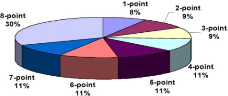
Fig. 4. Average distribution of transform lengths over the 16 test sequences which are listed in Table III.
zero-skipping is derived to increase the opportunity for the com-putation and memory access reduction compared with the tradi-tional zero-skipping schemes. These two features are explained in detail in the following two subsections.
A. Multiplication Sharing by Transform Matrices’ Numerical Properties
The numerical properties exploited in this work are different from the traditional ones. The traditional numerical properties have been explored in many fast algorithms designed for the 1-D DCT or IDCT [21]. However, most of these researches focus
on with and only consider the
optimiza-tions for a particular fixed-length 1-D DCT/IDCT. For the 1-D variable-length DCT/IDCT, optimizing the design for different lengths results in more complex resource allocation and sched-uling. Neglecting the numerical properties of lengths other than 8-point avoids making a more complex design; however, it also reduces the opportunity for further resource sharing. According to the statistics on average distributions of different transform lengths shown in Fig. 4, the 8-point transform only accounts for 30% of all transforms, whereas other lengths account for 70% of all transforms. Hence, it is worth improving the resource sharing for transform lengths other than 8-point. Based on this statistic result, the numerical properties beyond the traditional ones for the fixed 8-point transform should thus be exploited.
To exploit the numerical properties, we have investi-gated -point 1-D DCT/IDCT transformation matrices for
. The properties are listed below.
a) Even columns are even-symmetric and odd columns are odd-symmetric in -point 1-D IDCT transformation ma-trices.
b) The values of column 0 of -point 1-D IDCT transfor-mation matrices are always .
c) In even-point matrices, the values of the upper or lower half part of all columns except column 0 are odd-sym-metric.
d) The values of column 3 of a 6-point matrix are .
e) The values of column 4 in an 8-point matrix are .
f) The values of column 0 and column 2 in a 4-point matrix are 0.5.
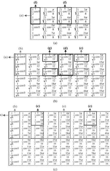
g) The values of column 2 in a 6-point matrix are 0.5. These properties are demonstrated by taking the 4-point, 6-point, and 8-point transform matrices as examples, as shown in Fig. 5. The coefficients which satisfy the properties are
Fig. 5. Variable-length 1-D DCT transform matrices demonstrating different numerical properties. (a) 4-point DCT/IDCT transform matrix. (b) 6-point DCT/ IDCT transform matrix. (c) 8-point DCT/IDCT transform matrix.
marked with their corresponding properties in parentheses. We chose these three lengths as examples because they exhibit all of the properties listed above. Other lengths of transform matrices also exhibit some of the numerical properties. Take , for instance. Numerical properties 1) and 2) can also be found in its transform matrices.
The numbers of multiplications for -point DCT/IDCT ma-trices are listed in Table I. The parentheses in this table mean the properties applied to obtain the number of multiplications. For instance, row 0 in an 8-point DCT/IDCT transform matrix has only one constant because of the property 2). As a result, ; only one multiplication is required as indicated in Table I. Note that, based on properties 6) and 7), the multiplication of 0.5 is replaced by using right shift. Based on these numerical properties, the common subexpressions sharing, scaling, and in-version are performed to reduce the number of multiplication. After applying these reductions, at most four multiplications are necessary at the same time, as indicated in Table I.
In addition to resource sharing, careful scheduling is done to minimize the clock cycle counts required to finish the 1-D DCT/ IDCT. Table II lists the processing schedule of input ,
TABLE I
NUMBER OFMULTIPLICATIONS INEACHROW OF THETRANSFORMMATRICES
TABLE II
PROCESSINGSCHEDULE OFN-POINT1-D DCT/IDCT
where the subscript is the length of the DCT/IDCT, and in-dicates the th input. The number in Table II represents . For example, when , and are processed in the first cycle, and are processed in the second cycle, and in the third. Similarly, an 8-point 1-D DCT can be com-pleted in six clock cycles using four multipliers. To compute a full 8 8 DCT, the proposed architecture requires 100 cycles to be complete. Since both the forward and inverse 1-D vari-able-length transforms use the same numerical properties found in the transform matrices, the schedules of input for both trans-forms are arranged to be the same. By sharing the same input schedule, the design of the SA-DCT/SA-IDCT’s multiplexers and demultiplexers can be shared.
B. Fine-Grained Zero-Skipping Scheme
Fine-grained zero-skipping offers more computation skip-ping than the traditional coarse-grained zero-skipskip-ping. In addition to computation reduction, the proposed fine-grained zero-skipping scheme also reduces the memory access at the same time. The traditional zero-skipping in [11], [15], and [16] is limited to row- or column-level granularity. When scalar zero coefficients are present, no computation or memory access can be skipped in a traditional vector-based coarse-grained zero-skipping scheme. In contrast, the fine-grained zero-skip-ping scheme proposed in this work decreases the level of granularity to a single coefficient instead of several coefficients in a row or column. This means that, whenever a coefficient is zero, we can skip its memory accesses and the computation for this zero-valued coefficient.
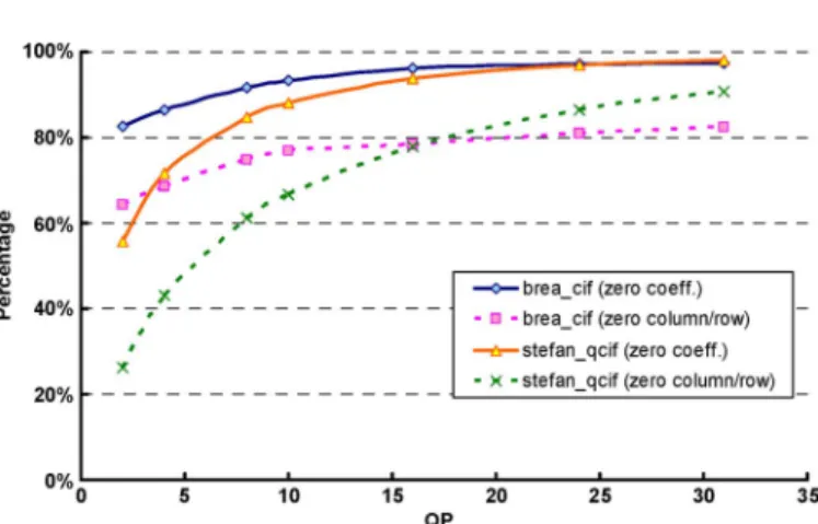
Table III shows the statistics of zero coefficients and zero rows/columns. These data are gathered from running the refer-ence software of MPEG-4 decoder [22] over 16 test sequrefer-ences listed in Table III. Moreover, the percentage of zero coefficients for the regular 8 8 IDCT is also investigated and listed in Table IV for reference. During the simulation, the quantiza-tion parameter (QP) is set to 10, which is relatively low com-pared with practical QP values. This implies that the percentage
TABLE III
PERCENTAGE OFZEROCOEFFICIENTS FORSA-IDCT
TABLE IV
PERCENTAGE OFZEROCOEFFICIENTS FOR82 8 IDCT
of zero coefficients is likely to be higher in practical QP set-tings. The simulation setting described here is also used in other statistic result in the rest of this paper.
According to Tables III and IV, the average percentage of zero coefficients for the SA-IDCT and regular 8 8 IDCT when are 89.9% and 90.7% respectively. Among the 16 test sequences, has the highest zero-coefficient per-centage while has the lowest zero-coefficient per-centage. Therefore, we further investigate the impact of different QP values based on these two extreme test sequences. Fig. 6 shows the percentage of the SA-IDCT zero coefficients and zero rows/columns with respect to different QP values for these two sequences. It can be seen clearly that, for lower QP values, both sequences exhibit a higher percentage of zero coefficient than the percentage of zero rows/columns. This finding can also be found in Fig. 7, which is the plot for the regular 8 8 IDCT on the percentage of zero coefficients and zero rows/columns. The extra percentage of zero coefficients offers the extra oppor-tunity to perform zero-skipping. Together with the aforemen-tioned comparison on the percentage of zero coefficients and
Fig. 6. Plot of zero coefficients and zero row/column vectors for the SA-IDCT.
Fig. 7. Plot of zero coefficients and zero row/column vectors for the IDCT.
Fig. 8. 2-D SA-DCT/SA-IDCT architecture.
zero rows/columns, the proposed zero-skipping scheme can ex-ploit 22.6% of extra zero-valued coefficients for skipping com-pared with the coarse-grained zero-skipping. The irregularity impact due to the fine-grained zero-skipping is solved by a low-cost zero-index table, which is part of the proposed architec-ture-level optimization. This will be explained in the next sec-tion.
V. ARCHITECTUREDESIGN
Fig. 8 shows the overall architectures of the proposed SA-DCT/SA-IDCT. Both of them are composed of a 1-D variable-length DCT or IDCT kernel, a transpose memory, an address generator, a multiplexer, and a demultiplexer. The main differences between the SA-DCT and SA-IDCT are the detailed architectures of the 1-D variable-length trans-form kernel and the transpose memory. For the SA-IDCT, the inverse transform and the extra support for the proposed fine-grained zero-skipping, such as the 64-bit zero-index table,
Fig. 9. Architecture of the 1-D variable-length DCT kernel.
Fig. 10. Reordering for the input of 8-point transform.
cause different architecture designs for the datapath of the 1-D variable-length transform kernel and transpose memory. A. One-Dimensional Variable-Length DCT/IDCT Kernel
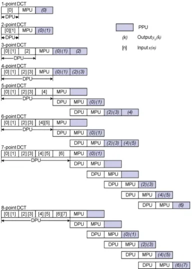
The architecture of the 1-D variable length DCT kernel is illustrated in Fig. 9. It is divided into three pipelined stages: data preparation unit (DPU), multiplication processing unit (MPU), and post-processing unit (PPU). Each stage is operated as follows.
• Data Preparation Unit (DPU)
The DPU stage performs two major tasks. The first task reorders the input samples by using two two-word LIFOs. The second task generates common subexpressions as in-puts for the next stage, the MPU stage. For example, take the worst case 8-point DCT operations. The reordering process is illustrated in Fig. 10. First, and are stored into the LIFOs, then and are stored;
when and are input, and are read
from the LIFOs to compute the common subexpressions
and , and then the
common subexpressions and
are processed in the same way. At the end, the common subexpressions are stored into the registers named add0 add3 and sub0 sub3.
• Multiplication Processing Unit (MPU)
The intermediate products of the common subexpressions and the transform coefficients are computed in the MPU. In addition to the multipliers, four adders are included to add the common subexpressions before multiplication. The reason for adding the common subexpressions is to group the subexpressions with the same multiplicand based on the numerical properties found in the transform matrices.
As a result, the multiplications can be shared, and thus reduces the number of multiplier to four, which is one less than that of Le’s feedforward architecture. Take the computation of in a 2-point DCT as an example of multiplication sharing. Since both the common
subexpres-sions and have to be
mul-tiplied with 0.5, they are grouped by adding both subex-pressions together before multiplying, therefore only one multiplication is required instead of two in
. Furthermore, two one-bit shifters are used instead of multipliers when the transform coefficients are 0.5. The hardware cost of two one-bit shifters is much less than that of one full multiplier. Note that there are four registers (reg0 reg3) in the MPU stage, which are illustrated in the lower part of the MPU in Fig. 9. These registers buffer the common subexpressions from the DPU stage which are not consumed by the adders and multipliers in the MPU. This allows the generation of the common subexpressions of the next row or column to continue in the DPU stage. As a result, the DCT operations of different rows or columns can be overlapped and thus improves the throughput.
• Post-Processing Unit (PPU)
In the PPU stage, the final transformed results are obtained by adding the intermediate products from the MPU stage. The additions are carried out by using three adders. To keep the output of the DCT in order, i.e., the output order shown in Fig. 11, four extra registers are used before the final output multiplexer in the PPU stage to reorder the results. The architecture of the 1-D variable-length IDCT is illus-trated in Fig. 12. It is also divided into three pipelined stages: multiplication processing unit (MPU), addition unit (ADU) and
Fig. 11. Input and output order of the 1-D DCT kernel.
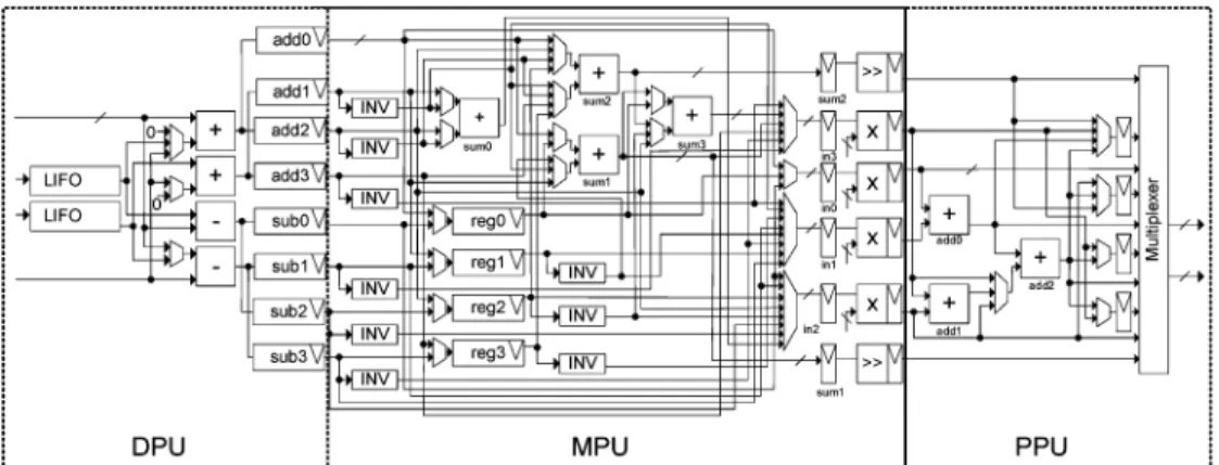
Fig. 12. 1-D variable-length IDCT architecture.
accumulation unit (ACU). Each stage is described and explained as follows:
• Multiplication Processing Unit (MPU)
Unlike the architecture of the 1-D variable-length DCT, the inputs are multiplied by the corresponding inverse trans-form coefficients to generate the common products in the first stage. For example, the first input of an 8-point
inverse transform coefficient is multiplied by in the
MPU. This common product is required for
the computation of all the eight inverse transform results . The numerical properties of the trans-form matrices mentioned earlier are also facilitated in the IDCT’s MPU stage. Therefore, only four multipliers and two one-bit shifters are used, which is the same as the number of multipliers and shifters of the MPU in the DCT. In addition, when the input is a zero coefficient, the mul-tiplication for this zero coefficient will be skipped, and a zero value would be generated in the next stage.
• Addition Unit (ADU)
The common products from the MPU are added to each other in the ADU stage. This stage includes four adders and five registers. The registers store the sums of the common products. Take the same 8-point case used previ-ously for example. The common products
and are added together for further computa-tion of and . If the multiplication in the MPU is skipped due to the zero input, the corresponding input in this stage will be zero.
• Accumulation Unit (ACU)
The sums of the common products in the ADU stage are accumulated to obtain the final inverse transform results in the ACU stage. Eight accumulators, each corre-sponds to an output, are incorporated to compute the in-verse-transformed values. Take the example of the 8-point IDCT,
, where stands for the accumulation operation. Hence, only five accumulations are required to compute . If the sum of the common products is determined to be zero, the computation of this sum of common product is skipped in the MPU and the ADU stages. Then the input of the corresponding accumulator is multiplexed to zero instead of the original input.
B. Auto-Aligned Transpose Memory and Zero Index Table In the conventional row-column decomposition of a 2-D DCT/IDCT, a transpose memory is required to store the in-termediate results of the first 1-D DCT/IDCT. As for the SA-DCT/SA-IDCT, an additional horizontal shift or vertical shift is also required to perform on these intermediate results. To ease the transpose and the alignment tasks, we propose the auto-aligned transpose memory architecture.
The auto-aligned transpose memory architecture combines the transpose memory and address pointer together to automati-cally align the data during the transform computation. Thus, no data shift is required. For the SA-DCT, we first logically parti-tion the transpose memory into eight rows and use eight address
pointers ( , ) to denote the addressing
of each rows. Then, when the first 1-D column DCT is com-puted, the result is directly written into the transpose memory addressed by the pointers. Each pointer is also increased by one when new data is written. After the whole 1-D transform is done, the data in these eight address pointers directly stand for the lengths of rows, and thus is ready for the second 1-D row DCT computation without explicit alignment. Take the DCT result
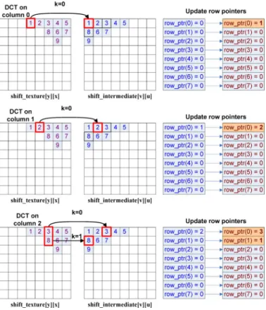
Fig. 13. Auto-alignment of the transpose memory using the addressing mode.
of column 2 in Fig. 13 for example. Before processing column 2, the results of column 0 and column 1 are already transposed and written into the buffer, the value of is also up-dated. After the transform for column 2, the first DCT result is written to the offset pointed by in row 0, and the second DCT result is written to the offset pointed by in row 1. The row pointers of rows 0 and 1 are also incremented after writing the results. By using the pointers, all information required for the second 1-D variable-length DCT is generated and all intermediate coefficients are auto-aligned to the correct positions. For the alignment in the SA-IDCT, the whole operation is similar to that in the SA-DCT, except that column pointers are updated instead of row pointers.
Although the proposed transpose memory supports the auto-alignment for DCT/IDCT computation, the shifting of the input pixels to align to the top in the SA-DCT (S1 in Fig. 2) or the shifting of the reconstructed pixels to their original locations (IS-5 in Fig. 3) are assumed to be handled externally.
In addition to the auto-alignment, to support zero-skipping in the proposed SA-IDCT architecture, the address generator in the transpose memory must be able to calculate the number of zero-valued intermediate coefficients for the second 1-D SA-IDCT. Hence, the transpose memory has a zero-index table with 64 bits to record whether each intermediate coefficient in a block is zero or not. The zero-index table is reset to zero each time a new block is to be processed. The proposed SA-IDCT archi-tecture only writes the nonzero term into the transpose memory, then it changes the value of the bit at the corresponding posi-tion in the zero-index table from zero to one. As a result, using the proposed zero-index table to calculate zero information not
only reduces the computation complexity from 16 bits to 1 bit, but also can decrease the routing complexity, the number of mul-tiplexers, and the power consumption.
VI. IMPLEMENTATIONRESULTS
The proposed SA-DCT and SA-IDCT architectures are both synthesized from Verilog RTL design using UMC 0.18 m 1P6M CMOS technology [23]. The SA-DCT synthesized design has a gate count of 26 657 (including the transpose memory). When the SA-DCT synthesized design is clocked at 100 MHz, the maximum average throughput is 65.75 Mpixels/s. As for the synthesized design of the proposed SA-IDCT archi-tecture, the synthesized gate count of the synthesized design is 31 473 (including transpose memory). When the SA-IDCT syn-thesized design is clocked at 62.5 MHz, the average throughput with the fine-grained zero-skipping enabled can reach up to 401.41 Mpixels/s. If the fine-grained zero-skipping is disabled, the design’s average throughput is 47.69 Mpixels/s. Note that the transpose memory is implemented with registers. Using registers instead of memories only increases the total area by 3%, which is only a small area overhead.
The core characteristics of the SA-DCT and SA-IDCT are compared with other architectures in Table V. The power con-sumptions of the proposed SA-DCT and SA-IDCT architec-tures are evaluated using Synopsys Prime Power. The power consumptions are reported from the gate-level simulation upon three frames of sequence. Since the percentage of zero coefficients in is the second lowest among the sequences, this power consumption can be regarded as a higher bound. The power consumptions are compared using the scaled power in Table V, which is scaled to match 0.18 m process, 1.8 V, and the required clock rate for CIF@30fps. It is believed that comparing with the scaled power should be more adequate than comparing the original power consumption directly.
To scale the power, the scaling process first calculates the required clock rate to achieve the decoding of CIF@30fps based on the original throughput; the clock scaling equation is shown as
Hz (3) Then, the power scaling is performed by the voltage scaling, process scaling, and frequency scaling shown as
m
mW (4) This scaling equation is derived from the dynamic power equa-tion , where V is the supply voltage, C is the capaci-tance, and F is the working frequency. By assuming that the ca-pacitance is linear with the square of the process parameter, the power equation becomes , where is the process parameter and k is a constant. By using this equation, the ratio of
TABLE V
COMPARISON OFSA-DCT/IDCT CORE CHARACTERISTICS
the power in 0.18 m process and in the original process repre-sents the scaling factor. The scaled power can then be estimated by multiplying the power scaling factor with the original power. We take the power scaling of Xanthopolous’s design as an example. There are 30 frames of 22 18 YUV 8 8 blocks that have to be processed within one second, where each block has 64 pixels. The cycle-throughput of Xanthopolous’s design is one pixel per cycle. Hence, the required clock rate of Xan-thopolous’s design to decode CIF@30fps would be
pixels/s
pixel/cycle MHz
and the scaled power is
mW
The comparison of the core characteristics of the SA-DCT and SA-IDCT are explained in the following two subsections. A. Comparison of SA-DCT
The often-cited design for the fixed-size DCT/IDCT pro-posed by Madisetti [10] is also listed for reference. We will use the cycle-throughput to compare the computation speed among the architectures. This cycle-throughput is defined as the number of pixels processed within one clock cycle; hence, the cycle-throughput is independent of the clock rate
used. Madisetti’s architecture achieves the highest average cycle-throughput among the compared architectures. This is because Madisetti’s design only supports the fixed 8-point DCT/IDCT, and therefore the multipliers can be hardwired to carry out constant multiplications. In contrast, using full multipliers constrains the maximum clock frequency of all of the other designs except for Chen’s ALU-based design. However, Chen’s approach focuses on a very low-cost archi-tecture. Consequently, its cycle-throughput is very low due to the use of only one single adder. Therefore, the comparison is focused on comparing the proposed SA-DCT architecture with Le’s feedforward and Tseng’s SA-DCT architectures. The cycle-throughput of the proposed architecture is very close to Tseng’s, which outperforms the rest of the SA-DCT architectures listed in Table V. Nevertheless, the proposed SA-DCT architecture requires the fewest number of multipliers compared with Le’s and Tseng’s architectures, whereas the number of adders for the proposed architecture is the same as Le’s. The reduced number of multipliers also reduces the power consumption of the proposed SA-DCT when it is compared with Tseng’s design.
Two factors enable the cycle-throughput of the proposed SA-DCT architecture to outperform Le’s design. One factor is that our design can support more than one pixel per clock cycle for input and output. This is reasonable when a wider system bus is employed. The other factor is that the DCT operations on consecutive rows or columns can be overlapped because of the four extra registers in the MPU stage. As for Le’s design, the
DCT operation of the next row or column can only start when the DCT operation of the current row or column is finished.
In summary, the proposed SA-DCT architecture achieves a comparable cycle-throughput using fewer multipliers and fewer total gate count. This indicates that the proposed SA-DCT ar-chitecture is a more cost-effective arar-chitecture compared with Le’s and Tseng’s.
B. Comparison of SA-IDCT
The comparison for the SA-IDCT architectures shows that both the cycle-throughput and the power consumption of the proposed SA-IDCT architecture outperform other architec-tures listed in Table V. Due to the benefits of the fine-grained zero-skipping scheme and efficient resource sharing, the av-erage cycle-throughput of the proposed SA-IDCT architecture is much higher than that of other architectures. However, to sup-port zero-skipping, extra cost overhead for the zero-index table is incurred. Therefore, the proposed SA-IDCT architecture has more gate count than the proposed SA-DCT architecture. Nevertheless, the hardware efficiency per cycle, which is de-fined as the ratio between the average cycle-throughput and the logic gate count, is one order higher than other SA-IDCT architectures. If the proposed zero-skipping is disabled, the worst case cycle-throughput is 0.77 pels/cycle; the hardware efficiency per cycle without zero-skipping is still higher than those of Le’s and Tseng’s architectures.
The greatly increased average cycle-throughput and the zero-skipping scheme also benefit the power consumption of the pro-posed SA-IDCT architecture. On one hand, the increased cycle-throughput enables the opportunity of using a lower clock rate to achieve the same throughput requirements for different profiles and levels and thus lowers the power consumption. On the other hand, zero-skipping skips the memory accesses and computa-tions for zero-valued coefficients and thus saves power. There-fore, the proposed SA-IDCT is capable of achieving the least power consumption using the least clock rate among the com-pared architectures while decoding CIF@30fps.
With the efficient resource sharing and zero-skipping schemes, the proposed SA-IDCT architecture outperforms other architectures in terms of both cycle-throughput and power while its cost remains comparable to other similar ar-chitectures. In summary, the proposed SA-IDCT architecture is more energy-efficient and cost-effective than other compared architectures.
VII. CONCLUSION
This paper presents the SA-DCT and SA-IDCT architec-tures that can efficiently cope with the complexity that arises due to the variable-length nature. The approach includes al-gorithm-level optimizations and architecture design. In the algorithm-level optimizations, the numerical properties of the transform matrices beyond the traditional 8-point transform are explored. Moreover, a fine-grained zero-skipping scheme is proposed for SA-IDCT. Based on the analysis of zero coefficients, the fine-grained zero-skipping scheme can skip more memory accesses and computations of zero coefficients than the vector-based coarse-grained zero-skipping can. In the
architecture-level design, the proposed 1-D variable-length DCT/IDCT kernel architectures are designed based on the numerical properties of various lengths, resource sharing, and careful scheduling to improve the cycle-throughput and the hardware efficiency per cycle. In addition, an auto-aligned transpose memory using row and column pointers instead of shifting is designed to deal with the transpose operation for the data of different lengths.
The implementation result shows that the proposed architec-tures have fewer gate counts than other existing architecarchitec-tures while having comparable or higher cycle-throughputs. Hence, we believe that the proposed SA-DCT and SA-IDCT ar-chitectures have better hardware efficiency per cycle when compared with others. The proposed fine-grained zero-skip-ping scheme can also greatly improve the cycle-throughput of the SA-IDCT while effectively reducing the memory accesses in the SA-IDCT. The power consumption of the proposed SA-IDCT using UMC 0.18 m technology is 0.14 mW when it is decoding for CIF@30FPS. Therefore, the proposed SA-IDCT can be considered as an energy efficient architecture. However, the proposed dedicated variable-length DCT/IDCT architecture may not be suitable for fixed-length integer transforms which are regular and require no multiplication.
REFERENCES
[1] M. Gilge, T. Engelhardt, and R. Mehlan, “Coding of arbitrarily shaped image segments based on a generalized orthogonal transform,” Signal
Process. Image Commun., vol. 1, pp. 153–180, Oct. 1989.
[2] T. Sikora, “Low complexity shape-adaptive DCT for coding of arbi-trarily shaped image segments,” Signal Process. Image Commun., vol. 7, pp. 381–395, Nov. 1995.
[3] R. Stasinski and J. Konrad, “A new class of fast shape-adaptive or-thogonal transforms and their application to region-based image com-pression,” IEEE Trans. Circuits Syst. Video Technol., vol. 9, no. 1, pp. 16–34, Feb. 1999.
[4] Information Technology–Coding of Audio-Visual Objects , Dec. 2001. [5] P. Kauff, K. Schuur, and M. Zhou, Experimental Results on a Fast SA-DCT Implementation ISO/IEC JTC1/SC29/ WG11 MPEG98/M3640, Jul. 1998.
[6] K. J. R. Liu, C. T. Chiu, R. K. Kolagotla, and J. F. Jala, “Optimal unified architectures for the real-time computation of time-recursive discrete sinusoidal transforms,” IEEE Trans. Circuits Syst. Video Technol., vol. 4, no. 2, pp. 168–180, Apr. 1994.
[7] T. Le and M. Glesner, “Flexible architectures for DCT of variable-length targeting shape-adaptive transform,” IEEE Trans. Circuits Syst.
Video Technol., vol. 10, no. 12, pp. 1489–1495, Dec. 2000.
[8] P. C. Tseng, “Design and implementation of reconfigurable discrete cosine transform processor with shape-adaptive capability,” Master’s thesis, Dept. Electron. Eng., National Taiwan Univ., Taipei, Taiwan, R.O.C., Jun. 2001.
[9] M. Owzar, M. Talmi, G. Heising, and P. Kauff, Evaluation of SA-DCT Hardware Complexity ISO/IEC JTC1/SC29/ WG11 MPEG99/M4407, Mar. 1999.
[10] A. Madisetti and A. N. Willson, Jr., “A 100 MHz 2-D 82 8 DCT/IDCT processor for HDTV applications,” IEEE Trans. Circuits Syst. Video
Technol., vol. 5, no. 2, pp. 158–165, Apr. 1995.
[11] T. Xanthopolous and A. Chandrakasan, “A low-power IDCT macrocell for MPEG-2 MP@ML exploiting data distribution properties for min-imal activity,” IEEE J. Solid-State Circuits, vol. 34, no. 5, pp. 693–703, May 1999.
[12] C.-Y. Pai, W. E. Lynch, and A. J. Al-Khalili, “Low-power data-de-pendent 82 8 DCT/IDCT for video compression,” Proc. IEE Vision,
Image and Signal Process., vol. 150, no. 4, Aug. 22, 2003.
[13] S.-O. Bae and S.-J. Min, “A computationally efficient IDCT al-gorithm,” in Proc. Midwest Symp. Circuits Syst., 1997, vol. 2, pp. 973–976.
[14] S.-T. Lin, “Analysis and design of a high-throughput two dimension inverse scan discrete cosine transform processor,” M.S. thesis, Dept. Electron. Eng., National Chiao Tung Univ., Hsinchu, Taiwan, R.O.C., Jun. 2000.
[15] C.-C Lin, H.-C. Chang, K.-H. Chen, and J.-I. Guo, “Reconfigurable low power MPEG-4 texture decoder IP design,” in Proc. IEEE Asia-Pacific
Conf. Circuits Syst., Dec. 2004, pp. 153–156.
[16] N. August and D. S. Ha, “On the low-power design of DCT and IDCT for low bit-rate video codecs,” in Proc. IEEE Int. Conf. ASIC/SOC, Sep. 2001, pp. 203–207.
[17] C. Loeffler, A. Lifhtenberg, and G. S. Moschytz, “Practical fast 1-D DCT algorithm with 11-multiplications,” in Proc. ICASSP, May 1989, vol. 2, pp. 988–991.
[18] K.-H. Chen, J.-I. Gua, J.-S. Wang, C.-W. Yeh, and T.-F. Chen, “A power-aware IP core design for the variable-length DCT/IDCT tar-geting at MPEG4 shape-adaptive transforms,” in Proc. IEEE ISCAS, May 2004, vol. 2, pp. 141–144.
[19] R.-C. Ju, J.-W. Chen, J.-I. Guo, and T.-F. Chen, “A parameterized power-aware IP core generator for the 2-D 82 8 DCT/IDCT,” in Proc.
IEEE ISCAS, May 2004, vol. 2, pp. 769–772.
[20] K.-H. Chen, J.-I. Guo, J.-S. Wang, C.-W. Yeh, and J.-W. Chen, “An energy-aware IP core design for the variable-length DCT/IDCT tar-geting at MPEG4 shape-adaptive transforms,” IEEE Trans. Circuits
Syst. Video Technol., vol. 15, no. 5, pp. 704–715, May 2005.
[21] K. Rao and P. Yip, Discrete Cosine Transform: Algorithms, Advantages
and Applications. London, U.K.: Academic, 1990.
[22] MPEG-4 Video Verification Model Version 18.0 ISO/IEC JTC1/SC29/ WG11 N3908, Jan. 2001.
[23] UMC Free-of-Charge Libraries [Online]. Available: http://www.umc. com/english/design/b_3.asp
Hui-Cheng Hsu received the B.S. and M.S. degrees in electrical engineering from National Chiao-Tung University, Hsinchu, Taiwan, R.O.C., in 2002 and 2004, respectively.
She is currently with MediaTek, Inc., Hsinchu. Her research interests include processor architecture, dig-ital signal processing, and video display systems.
Kun-Bin Lee (M’05) received the B.S. degree in electrical engineering from National Sun Yat-Sen University, Taiwan, R.O.C., in 1996, and the M.S. and Ph.D. degrees in electronics engineering from National Chiao-Tung University, Hsinchu, Taiwan, R.O.C., in 1998 and 2003, respectively.
He is currently with MediaTek, Inc., Hsinchu. His current research interests include processor architec-ture, digital signal processing, video coding systems, and system-level exploration with a focus on data transfer optimization and memory management for image and video applications.
Dr. Lee is a member of Phi Tan Phi. In 2004, he was the recipient of the Long-Term Paper Award from Acer, the Professor Wen-Zen Shen Thesis Award from Taiwan IC Design Society, and the Outstanding Design Award of University LSI Design Contest from ASP-DAC. In 2005 and 2006, he received the Outstanding Paper Award from MediaTek.
Nelson Yen-Chung Chang (S’06) received the B.S. degree in electrical engineering from National Tsing-Hua University, Hsinchu, Taiwan, R.O.C., in 2000, and the M.S. degree in electronic engineering from National Chiao-Tung University, Hsinchu, in 2002. He is currently working toward the Ph.D. degree at National Chiao-Tung University.
His research interests include VLSI signal pro-cessing, video codec VLSI design, and system-level design. Currently, he is engaged in real-time ad-vanced stereo vision system research.
Tian-Sheuan Chang (S’93–M’06–SM’07) received the B.S., M.S., and Ph.D. degrees in electronics engineering from National Chiao-Tung University, Hsinchu, Taiwan, R.O.C., in 1993, 1995, and 1999, respectively.
He is currently with the Department of Electronics Engineering, National Chiao-Tung University, as an Assistant Professor. From 2000 to 2004, he was with Global Unichip Corporation, Hsinchu. His research interests include IP and SOC design, VLSI signal processing, and computer architecture.