義守大學
材料科學與工程學系
碩士論文
以奈米壓痕研究單晶磷化銦之變形
機制與行為
Deformation behaviors and mechanisms of
single-crystal InP by nanoindentation
研 究 生: 劉弟如
指導教授: 簡賸瑞 博士
以奈米壓痕研究單晶磷化銦之變形
機制與行為
Deformation behaviors and mechanisms of
single-crystal InP by nanoindentation
研
究
生 : 劉弟如
Student:Ti-Ju Liu
指導教授 : 簡賸瑞
Advisor:Sheng-Rui Jian
義 守 大 學
材料科學與工程學系
碩士論文
A Thesis
Submitted to Department of Materials Science & Engineering
I-Shou University
in Partial Fulfillment of the Requirements
for the Master degree
in
Materials Science & Engineering
December , 2015
Kaohsiung, Taiwan, Republic of China
以奈米壓痕研究單晶磷化銦之變形
機制與行為
摘 要
本研究中,運用奈米壓痕儀、微拉曼儀、掃描電子顯微鏡、聚焦離
子束以及穿透式電子顯微鏡研究單晶 InP(100)的奈米機械性質與變形行
為與機制。
單晶 InP(100)的硬度和楊氏模數是利用奈米壓痕儀中的連續接觸剛
度方式進行量測。
奈米壓痕的實驗結果:可發現多數個斷點現象出現在力—位移曲線
之負載部分。此外,微拉曼分析受壓痕影響之單晶 InP(100)亦無發現相
變化的存在。
利用穿透式電子顯微術以及擇區繞射分析,可清楚觀察差排沿著滑
移系沿著{0001}基面與錐體平面
{1011}上相互交錯。
進一步,以差排理論估算受壓痕影響之單晶 InP(100)之差排數目,
以期可以與實驗上作一互補的驗證。另外,單晶 InP(100)之破裂行為與
破裂強度亦在本研究中探討。
Abstract
In this study, the nanomechanical characteristics of single-crystal InP(100)
are investigated by using nanoindentation, micro-Raman, scanning electron microscopy (SEM), focused ion beam (FIB) and transmission electron microscopy (XTEM) techniques. Moreover, the hardness and Young’s modulus of single-crystal InP(100) are measured using a Berkovich nanoindenter operated with the continuous contact stiffness measurements (CSM) mode. The multiple “pop-ins” are observed in the load-displacement curve with increasing indentation load in a random fashion. And, no evidence of phase transformation is revealed by micro-Raman, the cross-sectional TEM (XTEM) and selected area diffraction (SAD) analyses. The nucleation of dislocations propagating along the slip systems lying on the {0001} basal planes and the {1011} pyramidal planes are observed in XTEM images. Based on this scenario, an energetic estimation of dislocation numbers is calculated in indented single-crystal InP(100) using classical dislocation theory. In addition, Berkovich nanoindentation-induced fracture toughness and cracking behaviors of single-crystal InP(100) are also discussed.
Acknowledgement
感謝指導教授簡賸瑞教授一直以來的肯定及照顧,不論在學業或論文寫作上給 予細心指導及傳授,謝謝您總是替我們在職的學生著想,讓我們可以工作及學業兼 顧。 謝謝兩位口試委員廖英彥教授及顏政佑教授撥空前來指導論文。在求學的這段 期間,謝謝瓊枝(May 姐)、馨儀、雅惠、有你們在的地方,總是多了許多歡笑聲, 也謝謝王笙羽(班代),每次上課都會幫忙帶晚餐,我想幫我們帶晚餐應該就是你來 唸書最大的動力了。 在材料系當系助有 10 年之久,很謝謝曾經幫過我的老師、系上的學生及系友們 (人數眾多無法一一寫出),有你們的幫忙讓我能以最快的速度完成學校所交辦的工 作,也因為有大家的幫忙,讓我很傷腦筋的教學意見和一大堆問卷完成率都能以最 快的速度達標。 在入學那年也是自已工作職務異動,很謝謝惠媚姐、雅慧、鍾姐,沒有你們的 幫忙和傾聽,我想我現在應該還無法適應新的工作環境,來義守工作最大的收獲就 是能認識你們。 謝謝招生組的工作伙伴,英文嚇嚇叫的主任:黃一正、數據高手:趙姐、組內 開心果:秀慧、工作效率一流的佩芳和細心穩重的洪菱,還好有大家的協助,讓我 能更快的進入狀況,最優秀的工讀生岱庭,有你的協助讓招生組的大家工作減輕了 不少。 謝謝曾經幫忙過我的大家,認識你們真好~Content
Chinese Abstract ... I English Abstract ... II Acknowledgement ... III Content ... IV Figures content ... V Chap1 Introduction ... 1Chap2 The methodology of nano indentation ... 5
2-1 Prepare TEM sample by using FIB ... 7
Chap3 Experimental details ... 8
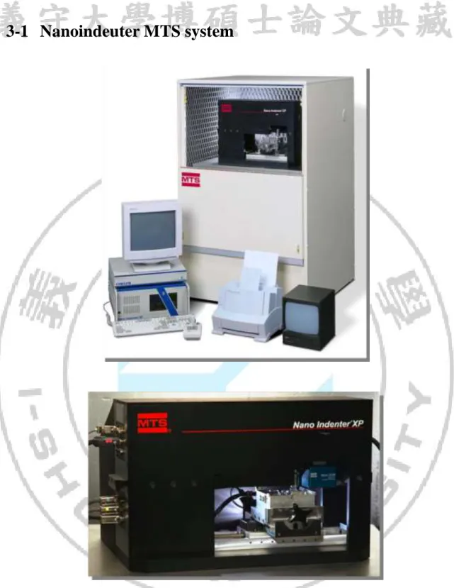
3-1 Nanoindeuter MTS system... 9
3-2 Scanning Electron Microscopy ... 10
3-3 Microscopes Raman Spectrometer ... 11
3-4 Trausmission Election Microscopy ... 12
3-5 Focused Ion Beam ... 13
Chap4 Results and Discussion ... 16
4-1 Nanoindentation tests ... 16
4-2 Indentation-induced crack behavior ... 20
4-3 micro-Raman analysis ... 24
4-4 Indentation-induced dislocations from TEM observations ... 26
4-5 Homogeneous dislocations nucleation ... 29
Chap5 Conclusion ... 33
Figures content
Figure1-1 The process schematics of TiO2/InP heterojunction solar cell on
fabrication ... 3
Figure1-2 Waveguide structures of an InP-based quantum-cascade lasers (QCL) .. 4
Figure 3-1 Nanoindeuter MTS system ... 9
Figure 3-2 Scanning Electron Microscopy ... 10
Figure 3-3 Microscopes Raman Spectrometer ... 11
Figure 3-4 Trausmission Election Microscopy ... 12
Figure 3-5 Focused Ion Beam ... 13
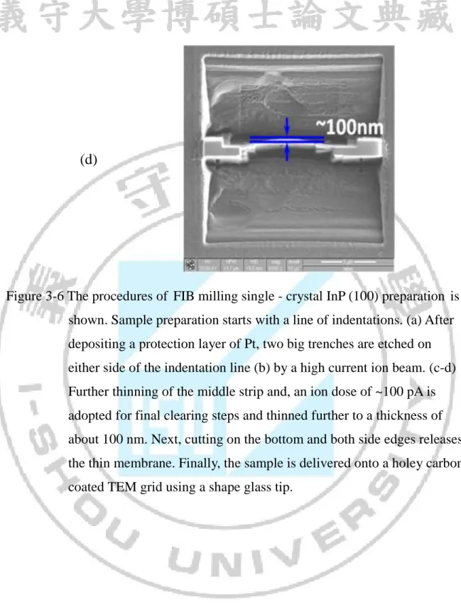
Figure 3-6 The procedures of FIB milling single - crystal InP (100) preparation is shown. Sample preparation starts with a line of nanoindentations. (a)After depositing a protection layer of Pt, two big trenches are etched on either side of the indentation line (b) by a high current ion beam.(c-d) Further thinning of the middle strip and, an ion dose of ~ 100 pA is adopted for final clearing steps and thinned further to a thickness of about 100 nm. Then, cutting on the bottom and both side edges releases the thin membrane. Finally, the sample is delivered onto a holey carbon coated TEM grid using a shape glass tip. ... 15
Figure 4-1 Nanoindentation results: (a) a load-displacement curve of single-crystal InP(100); (b) hardness-displacement, and (c) the Young’s modulus-displacement curves for single-crystal InP(100) ... 19
Figure 4-2 (a) The cyclic load-displacement curves obtained at an indentation load of 150 mN for single-crystal InP(100). Notice that the multiple “pop-ins” events are observable in the load-displacement curves (see the arrows); (b) SEM micrograph on an “indented” single-crystal InP(100) showing the cracking along the edges of the Berkovich indentation subjected to an indentation load of 150 mN ... 23 Figure 4-3 SEM micrograph on an “indented” single-crystal InP(100) showing
the cracking along the edges of the Berkovich indent at an indentation loadof 80 mN. The micro-Raman spectra of single-crystal InP(100) taken on the pristine surface and after
Berkovich nanoindentation. ... 25 Figure 4-4 An indented single crystal InP(100) under an indentation load of 150
mN: (a) Bright-field XTEM observation. Schematic representation of the Berkovich indentation-induced plastic zone: the rosette arms are denoted at both sides as the roof-shape zone. The projection of the converging and diverging slip planes in the (110) plane; (b) SAD pattern results of sample underneath the Berkovich indenter. .... 28 Figure 4-5 The corresponding first pop-in event (see the arrow) from Figure 4-2
(a)is zoomed in, where the plastic strain work is denoted as, Wp
(critical loading times the sudden incremental displacement at
Chap 1 Introduction
Indium Phosphide, (InP), is a III-V semiconductor material with a direct band gap[1]. InP is an important semiconductor material for several applications, such as optoelectronic devices; that is, solar cells (please see Figure 1-1)[2,3] ,
quantum-cascade lasers (the QCL structure, please see Figure 1-2) [4,5] and the
InP-based micro-electro-mechanical systems devices[6,7].
The developments of micro/nanotechnology have been achieved based on the semicorduotor materials and surface science. In the past, they have been mostly characterized in terms of their optical, electrical and magnetic characterization. However, the structural and micro/nanotechnology mechanical characteristics are also as important. Currently, there is a need to develop new method to characterize the mechanical response of nano-structured materials and various thin films. This is because that the traditional methods such as tensile, compression and microindentation techniques are unsuitable, since they do not scale well into nanoscale.
According the above-mentioned, the applications of InP-based materials to the various devices are focused on their optical and electrical properties; on the contrary the mechanical properties of semiconduotor materials have not drawn multidisciplinary attentions. The successful fabrication of micro/nano-devices based on the single-crystal InP(100) requires an understanding of the mechanical characteristies in addition to the optical and electrical properties. Because of the contact loading during packing or devices applications, the performances of these related devices can be demeaned. Therefore, it is of interest to investigate the mechanical properties of semiconductor materials for micro/nano-devices applications.
It is well known that the mechanical characteristics of materials are size-dependent. In recent years, the role of materials structural changes under
contact loading was largely underestimated because of the difficulties in structural properties of nano-structured materials and various thin films affected by the local contact damage. The advent of Nano-scale indentation apparatus, that is, NANOINDENTION and, the subsequent development of the underlying science may potentially denote the physical and scientific phenomena of all contact conditions. Nanoindentation measurements are now widely used to obtain the mechanical characterizatious of nano-structured materials and the various thin films.
Nanoindentation technique has been used to investigate the deformation behaviors and mechanisms of semiconductor materials [8-10] and various thin films [11-18]. In addition to that, the molecular dynamics (MD) simulations have been
developed to analyze the atomic interactions for indented various materials and thin films subjected nanoindentation processes[19-22]. Moreover, the mechanical
properties of semiconductor materials and films, such as the hardness and elastic modulus, have been measured by means of this technique. It appears meaningful to extend the nanoindentation to single-crystal InP(100), in merit of both scientific research and industrial applications.
However, this technique itself does not provide the information of deformation behaviors and mechanisms subjected to nanoindentation. The focused ion beam technique, which is now widely used for a range of materials applications[23-25], can be applied to readily image and prepare the cross-sections of sample. The FIB can be used in the preparation of transmission electron microscopy (TEM) foil samples, especially from deformed that have been local damaged.
Previously studies[26-31], although both micro-Raman and plan-view TEM
techniques have been analyzed the nanoindentation-induced phase transition and /or dislocations propagation along the horizontal direction of semiconductor materials and thin films, they cannot distinguish the phase changes inside the deformed zone along the vertical direction. Herein, in this article, the motivation for this study is to measure the nanomechanical properties, such as hardness and
elastic modulus, of single-crystal InP(100); in addition to investigate nanoindentation-induced deformation behaviors and mechanisms, cracking events, by means of the nanoindentation and microscopical techniques, including scanning electron microscopy (SEM), micro-Raman, focused ion beam (FIB), transmission electron microscopy (TEM) and selected area diffraction (SAD) pattern techniques, of single-crystal InP(100).
Figure1-1 The process schematics of TiO2/InP heterojunction solar cell fabrication
Figure1-2 Waveguide structures of an InP-based quantum-cascade lasers (QCL) [33].
Chap 2 The methodology of nano indentation
The nanoindentation measurements were performed on a Nanoindenter MTS NanoXP® system (MTS Cooperation, Nano Instruments Innovation Center, TN,
USA) with a diamond pyramid-shaped Berkovich tip, whose radius is about 50 nm. The nanomechanical properties of single-crystal InP(100) were measured by using a continuous stiffness measurements (CSM) technique [34]
. In
nanoindentationtests, A small sinusoidal load with known frequency and amplitude was superimposed onto the quasi-static load. It results in a modulation of the indenter displacement that is phase shifted in response to the excitation force. The stiffness, of the material(S ), and the damping(wC), along indentation loading can be respectively calculated using Eq. (1) and Eq (2) expressed below. The hardness and elastic modulus are calculated by putting the obtained stiffness data into Eq. (3) and Eq. (4)The hardness and modulus as a function of the penetration depth are measured for a single loading/unloading cycle[35].
1 1 2 max ) ( cos ) ( 1 f s K mw K w h P S (1) sin ) ( 0 w h P wC (2) c A P H max (3) S A v E c 1 2 1 2 (4)
where Pmax and h(w) are denoted as the driving force and the displacement of
indenter, respectively; is the phase angle between Pmax and h(w); m is the mass of the indenter column; Ks is spring constant at the vertical direction; Kf
is frame stiffness; m , Ks and Kf are all constant values for specified indentation system; w is angular speed which equals to 2f ; f is the driven frequency of the ac signal of 45 Hz for this work, which is used to avoid the sensitivity to thermal drift; the loading resolution of the system was 50 nN; v is Poisson’s ratio for the measured materials; and Ac is contact area when the
material in contact with indenter being loaded atPmax.
The area function, which is used to calculate contact area (Ac) from the contact
depth (hc) was carefully calibrated by using fused silica as the standard sample prior to the nanoindentation experiments. The nanoindentation tests were carried out in the following sequence: first, the Berkovich indenter was brought into contact with the surface at a constant strain rate of 0.05 s-1 until 200 nm of
penetration was achieved. Then the load was held at the maximum value for 10 sec to determine the creep behaviors. They the Berkovich indenter was withdrawn from the surface at the same rate until 15 % of the maximum load was reached. This constant strain rate was chosen such that the strain-hardening effect can be avoided during the tests. At least 50 indents are performed on each sample. The indentatious are sufficiently spaced to prevent from mutual interactions.
2-1 Prepare TEM sample by using FIB
After indentation to a larger indentation load, the cross-sectional transmission electron microscopy (XTEM) samples of the semiconductor materials are prepared by using the lift-out technique using a dual-beam focused ion beam (FIB) station (FEI Nova 220). The technique for sample preparation using the FIB consisted of first milling two crosses alongside the indented area, serving as makers, and then depositing a layer of Pt to protect the area of interest from damages and implantation by the injected Ga+ ion beam. Materials was removed
from both sides of the selected area using an ion current of 5 nA, followed by successive thinning steps by reducing the ion current progressively from 3 nA to 300 pA until the foil is about 1µm thick. Subsequently, the bottom and one side of the foil are cut free while tilting the sample at an angle of 45º to the ion beam. A central area containing the indentation apex of a few micrometers in length is then chosen and thinned further to a thickness of 100 nm, leaving the side thicker areas relatively intact to prevent the foil from collapsing. Finally a small area of interest was selected and thinned until electron transparency was achieved. The transfer of sample from the sample holder to the TEM grid with a carbon membrane was made ex situ using the electrostatic force of a glass needle. The TEM samples are examined in JEOL-2010F TEM operating at an accelerating voltage of 200 kV. The details of FIB produces in preparing TEM sample can be found elsewhere[36].
Chap 3 Experimental details
The single-crystal InP(100) adopted in this work was purchased from Semiconductor Wafer Inc. The nanoindentation tests were performed on a Nanoindenter MTS NanoXP® system (MTS Cooperation, Nano Instruments
Innovation Center, TN, USA) with a diamond pyramid-shaped Berkovich-type indenter tip (face angle 65.3º), whose radius is about 50 nm, as shown in Figure 3-1.
For microstructural analyses, a 20 20 indent array with each indent separated by 20 m was produced by holding at the peak load of 150 mN for 10 s with the same loading/unloading rates for single-crystal InP(100). The indentations are observed using scanning electron microscopy (SEM), as shown in Figure 3-2. An indentation load of 150 mN is examined by using a micro-Raman spectrometer (Renishaw, UK) with an Ar+ laser (excitation wavelength 514.5 nm).
The size of the laser spot is about 1 µm, as shown in Figure 3-3.
After indentation to an indentation load of 150 mN, the transmission electron microscopy (TEM, FEI TECNAI G2 TEM, as shown in Figure 3-4)
samples of single crystal InP(100) were prepared by the lift-out technique using a dual-beam focused ion beam (FIB) station (FEI Nova 220), as shown in Figure 3-5. The technique for sample preparation using the FIB consisted of first milling two crosses alongside the indented area, acting as makers, and then depositing a 1 µm thick layer of Pt to protect the area of interest from Ga+ ion beam damage and
3-1 Nanoindeuter MTS system
3-2 Scanning Electron Microscopy
Model:Hitachi-S3400,EDS Model:HORIBA 1.0.5~30KV
2.Electronic Source:Tungsten 3.Magnification:X 35 ~ X 50k
4.High resolution can be observed: Resolution :1.5nm 5.EDS analysis:92≧ Atomic ≧ 5
6.Automatic function:Focus, aberration correction, brightness, contrast。 Main accessories:(1) EDX。
3-3 Microscopes Raman Spectrometer
Specifications
1. Light Source:Laser 514nm/633nm/785nm 2. Frequency Range:0cm-1~4000cm-1 3. Depth and Mapping Measurement 4. Sample Type:Solid and Liquid 5. Grating:1200/1800 gr/mm
6. Minimum Laser Spot Size:≦1um
3-4 Trausmission Election Microscopy
Model:FEI Tecnai G2 20 S-Twin, EDS Model:METEK
1.Accelerating voltage:200KV 2.Magnification:2250~1000kXc 3.Filament:LaB6
4.High-resolution image can be observed:Point Resolution: 0.248nm Line Resolution : 0.144nm 5.Spot size: ≧ 3nm
6.Double tilt specimen holder:X axis ± 400; Y axis ± 400 7.EDS analysis:92≧Atomic≧ 5
3-5 Focused Ion Beam
Model:FEI Nova 200
1. Electron source:Field emission type 2. Ion source:Ga Liquid metal ion source
3. Accelerationg voltage:Electron beam-0.5~30kV、Ion Beam-5~30kV 4. Image resolution:SEM-1.5NM、FIB-7nm
5. Working distance:0.50cm
6. Specimen size:diameter(1cm~2.5cm) x height(<0.50cm) 5.Working distance: 0.50cm
(a)
(b)
(d)
Figure 3-6 The procedures of FIB milling single - crystal InP (100) preparation is
shown. Sample preparation starts with a line of indentations. (a) After depositing a protection layer of Pt, two big trenches are etched on either side of the indentation line (b) by a high current ion beam. (c-d) Further thinning of the middle strip and, an ion dose of ~100 pA is adopted for final clearing steps and thinned further to a thickness of about 100 nm. Next, cutting on the bottom and both side edges releases the thin membrane. Finally, the sample is delivered onto a holey carbon coated TEM grid using a shape glass tip.
Chap 4 Results and Discussion
4-1 Nanoindentation tests
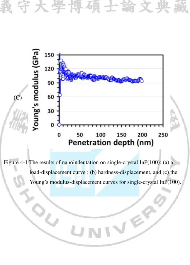
Figure 4-1(a) shows the typical nanoindentation curve analyzed for single-crystal InP(100) using CSM mode. The penetration depth into single-crystal InP(100) was about 200 nm with a peak load of ~4.5 mN. The hardness and Young’s modulus of single-crystal InP(100) can be calculated from the load-displacement records developed by Oliver and Pharr [37]. Moreover, with the CSM tests, the penetration depth dependence of the hardness and Young’s modulus of single-crystal InP(100) can be obtained, shown in Figures 4-1(b) and 4-1(c), respectively.
The hardness of single-crystal InP(100) remains nearly constant at 6.5±0.3 GPa with small variations, possibly associated with dislocation activities, as shown in Figure 4-1(b). Similarly, as shown in Figure 4-1(c), Young’s modulus of single-crystal InP(100) also displays a sudden drop occurring around the same penetration depth and then remains relatively constant at 108.2±5.6 GPa. The present results can be compared with the Ref.[38], which using the spherical
indentation. Our results (the hardness and Young’s modulus) is larger than the Bradby’s works, it can be assumed that the difference between these results are caused by the geometric shape of indent.
(a)
(b)
(C)
Figure 4-1 The results of nanoindeutation on single-crystal InP(100): (a) a load-displacement curve ; (b) hardness-displacement, and (c) the Young’s modulus-displacement curves for single-crystal InP(100).
4-2 Indentation-induced crack behavior
Figure 4-2(a) shows the load-displacement results obtained at an indentation load of 150 mN and deeper penetration up to 1600 nm. It can be found that the multiple pop-ins are significantly displayed over such a wide range of indentation load and penetration depth indicates the close relations to the plastic deformation of single-crystal InP(100). It is suggestive that the first pop-in phenomenon is not thermally activated, because the multiple pop-ins are randomly distributed on the loading curve Figure 4-2(a) and each curve is associated with the various stress rate which increases with the indentation loading. Instead, these phenomena are usually attributed to dislocation nucleation and propagation during loading as have been observed in a wide variety of materials[39-46]. Also, the reverse discontinuities
during unloading curve, the so-called “pop-out” pheaomeuon commonly observed in single-crystal si and has been attributed to pressure-induced phase transformation behavior[47-52] is not observed in this work.
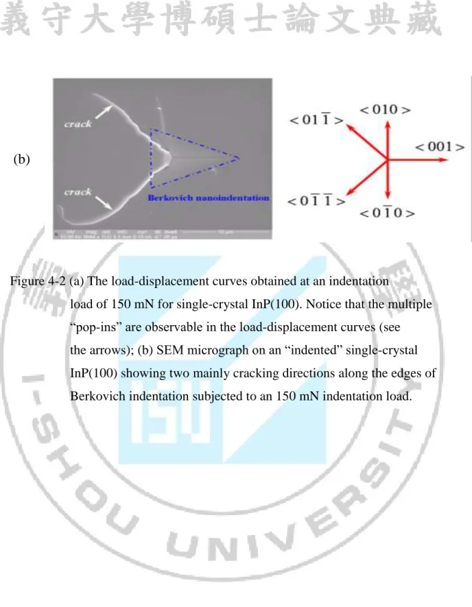
Figure 4-2(b) is a SEM image of indentation generated at an indentation load of 150 mN. The cracks have formed along the both sided corners of indentation and propagated in the radial directions. The paths of crack propagation are not in a straight line and the propagation directions are somewhat flexuous. Here, we can divide four directions in the crack propagation: 010, 011, 011 and
010 , respectively.
In addition, the fracture toughness (Kc) is another prominent mechanical
property, which can be determined by using the following expression[53]:
2 / 3 max 2 / 1 c P H E Kc , (4-1)
where β is an empirical constant which depends on the geometry of the indenter (0.016 for Berkovich indenter) and, c is the length of the radial crack trace on the
material surface after the Berkovich indenter is withdrawn.
In order to gain insight into crack induced the fracture energy (Gc) of single-crystal InP(100) was estimated based on the elastic modulus and fracture toughness using the following relation[54]:
E v K Gc c 2 2 1 , (4-2)
The obtained fracture toughness and the fracture energy, which is the energy required for a crack to propagate in the materials and films, are ~0.2 1/2
m
MPa and ~0.3 2
(a)
(b)
Figure 4-2 (a) The load-displacement curves obtained at an indentation
load of 150 mN for single-crystal InP(100). Notice that the multiple “pop-ins” are observable in the load-displacement curves (see the arrows); (b) SEM micrograph on an “indented” single-crystal InP(100) showing two mainly cracking directions along the edges of
4-3 micro-Raman analysis
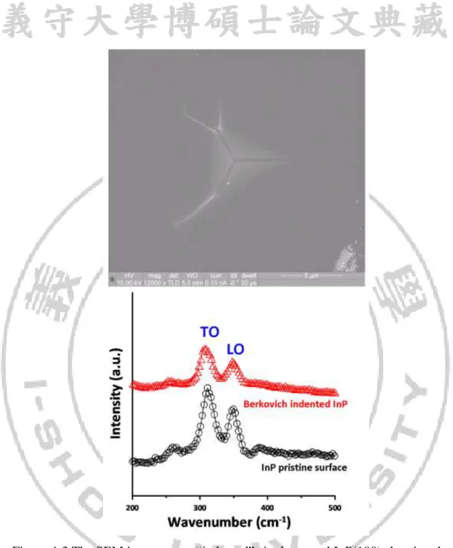
In Figure 4-3, the micro-Raman spectra for Berkovich indentation on single-crystal InP(100) at an indentation load of 80 mN are shown. The two spectra are significantly displayed before one nanoindentation and, after: the other taken at center of inden. The features of transverse optical (TO) and longitudinal optical (LO) peaks, respectively, at 309.7 cm-1 and 348.1 cm-1 are clearly observed in the pristine InP. It can be found that both TO and LO modes are slightly shifted to the higher wavenumbers via Berkovich nanoindentation, as shown in the center of indented area. The fact that the peak displacement is largest at the center of the indented area and decreases outward, indicating the compressive stresses is the mainly and important factor. Moreover, no extra peaks are observed in Figure 4-3, indicating that no phase transformation phenomena in the material have occurred.
Figure 4-3 The SEM image on an “indented” single-crystal InP(100) showing the cracking along the edges of the Berkovich indent at an indentation load of 80 mN. The micro-Raman spectra of single-crystal InP(100)
4-4 Indentation-induced dislocations from TEM observations
The plastic deformation process is very complex and further investigatious will be necessary to delineate what happens to single-crystal InP(100) as the Berkovich indenter penetrates into the single-crystal InP(100) surface. The nanoindentation-induced deformation mechanisms and behaviors will be discussed from XTEM observations in the following.
In Figure 4-4(a), a BF XTEM image of single-crystal InP(100) via an indentation load of 150 mN is displayed. It can be found that the Berkovich indentation-induced dislocations are significantly formed in the vicinity of indentation. In addition, the induced dislocation patterns formed are on different slip planes interact intensively with each other to form sessile dislocations. The slip bands are oriented at an angle of 54o to single-crystal InP(100) surface,
indicating that slip deformation of InP structure occurs within the {111} planes, which are vertical to the (110) plane in XTEM observation. Thereafter, the structure of the plastic zone is also display in Figure 4-4(a). The roof-shape zone has a square base whose both sides are parallel to the <110>-direction. The {111} sides of the pyramid intersect along the four <011>-direction inclined to the single-crystal InP(100) surface. Consequently, this Berkovich nanoindentation-induced plastic deformation structure is very consistent with the XTEM observations. The deformation behaviors and mechanisms of Berkovich indented single-crystal InP(100) can be found elsewhere[55].
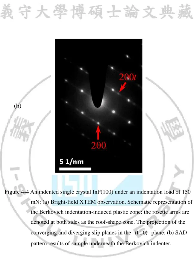
The selected area diffraction (SAD) pattern is taken from Figure 4-4(a), which shows the existence of twinning, as shown in Figure 4-4(b). In Figure 4-4(b), the intensity of the twin spots in SAD pattern is very strong, indicating that a high density of twins. In addition, there is no indication of the formation of cracks or other phases, so the Berkovich nanoindentation-induced deformation behaviors seem to proceed exclusively by the formation of twins in single-crystal InP(100).
(a)
(b)
Figure 4-4 An indented single crystal InP(100) under an indentation load of 150 mN: (a) Bright-field XTEM observation. Schematic representation of the Berkovich indentation-induced plastic zone: the rosette arms are denoted at both sides as the roof-shape zone. The projection of the converging and diverging slip planes in the (110) plane; (b) SAD pattern results of sample underneath the Berkovich indenter.
4-5 Homogeneous dislocations nucleation
Within the scenario of the dislocation nucleation and propagation mechanism, the first pop-in phenomenon naturally reflects the transition from perfectly elastic to plastic deformation. That is, it is the onset of plasticity in single-crystal InP(100). The critical shear stress (max ) under the Berkovich indenter at an indentation load,
*
P , where the load-displacement discontinuity occurs, can be determined by the equation[56]: 3 / 1 2 3 2 * max 6 31 . 0 R E P r , (4-3)
where R is the radius of indenter tip. Here, the max for single-crystal InP(100) is obtained about 2.3 GPa. We assume that this max is responsible for the homogeneous dislocation nucleation within the deformation region underneath the indenter tip.
It has been proposed that the first pop-in pheuomenon is associated with the homogeneous dislocation nucleation during nanoindentation processes. According to the classical dislocation theory [57], the shear stress required to
initiate plastic deformation depends on the plastic energy required to generate a dislocation loop. The free energy of a circular dislocation loop of radius (r), is defmed by:
2
2 r b r
F dis , (4-4)
where dis and b are deuoted as the line energy of dislocation loop and
the magnitude of Burgers vector (is about 0.4 nm) [58], respectively. And, is
the external shear stress acting on the dislocation loop.
energy required to create a dislocation loop in a defect-free lattice and is equal to the increase in lattice energy because of a formatted dislocation loop. The second term gives the work done by the applied stress ( ) as a result of the Burgers vector displacement and reflects the work done on the system to expand the dislocation. The line energy for a circular loop (dis), which results from the lattice strain in the vicinity of the dislocation for rrcore, is Following [59]: ln 4 2 1 2 8 2 core f f dis r r v v Gb , (4-5)
where G is the shear modulus of single-crystal InP(100) (is about 30 GPa)
[58] and
core
r is the radius of dislocation core. Using Equation (4-3) and Equation (4-5), the Equation (4-4) can be rewritten as following:
c core f f br r r r v v Gb F 2 2 2 4 ln 1 2 4 , (4-6)
The above-mentioned equation (Equation (4-6)) relates the material properties and experimentally observed pop-in load ( *
P ) to the free energy responsible for dislocation nucleation; in addition, c is the resolved shear stress of max on the active slip system [60]. The nucleation of a dislocation loop is
similar to the nucleation of a spherical new phase within a homogeneous matrix, where the corresponding function Fcontains terms with first and second power of r. Fhas a maximum at a critical radius (rc) above which the system gains
energy by increasing r. According to Eq. (5), this maximum energy is decreased with increasing load and a pop-in, i.e. the homogeneous formation of circular dislocation loop, becomes possible without thermal energy at F 0[61]. The
0
F condition allows c to be found Equation (4-4) and Equation (4-5) giving as c 2dis/br, and core core c r r e r 5 4 3 , (4-7)
Therefore, the value of rcore0.4nm is obtained. And, the rc 2.2nm can be
calculated from Equation (4-7).
The number of dislocation loops formed during the first pop-in can, thus, be estimated from the work-done associated. From the shaded area (Figure 4-5), the indentation-induced energy is estimated to be 10
10 Nm, implying that the umbers of 6
10 dislocation loops with critical diameter are formed during the Berkovich nanoindentation-induced first pop-in event. This number is low and is consistent with the scenario of homogeneous dislocation nucleation-induced pop-in even, instead of activated collective motion of pre-existing dislocations[62].
Figure 4-5 The corresponding first pop-in event from Figure 4-2(a) is zoomed in, where the plastic strain work is denoted as, Wp.
Chap 5 Conclusion
The nanomechanical properties, cracking behavior and phase transformation and/or dislocation patterns of nanoindeuted single-crystal InP(100) are investigated by using MTS Nanoindenter, SEM, micro-Raman and TEM/SAD techniques, respectively.
The mainly points are summarized:
1.Nanoindentation results: the hardness and Young’s modulus of single-crystal InP(100) obtained by CSM mode are 6.5±0.3 GPa and 108.2±5.6 GPa, respectively.
2.micro-Raman results: no evidence of phase transition is found in indented single-crystal InP(100).
3.The fracture toughness of single-crystal InP(100) is about 0.2 MPa·m1/2.
4.The nanoindentation-induced generation of dislocation loops associated with the first pop-in event is estimated to be in the order of 6
10 with a critical radius (rc 2nm).
Chap 6 References
[1]. V. Swaminathan, A.T. Macrabder, Materials Aspects of GaAs and InP
Based Structures, Englewood Cliffs, NJ: Prentice, 1991.
[2]. T.J. Coutts and S. Naseem, “High efficiency indium tin oxide/indium
phosphide solar cells”, Appl. Phys. Lett., vol.46, no.2, 1985, p.164.
[3]. X. Yin, C.Battaglia, Y. Lin, K. Chen, M. Hettick, M. Zhang, C.Y. Chen,
D. Kiriya and A. Javey, “19.2% efficient InP heterojunction solar cell
with electron selective TiO
2contact”, ACS Photonics, vol.1, no.12, 2014,
p.1245.
[4]. O. Malis, C. Gmachl, D.L. Sivco, L.N. Pfeiffer, A.M. Sergent and K.W.
West, “The Quantum Cascade Laser: A Versatile High-Power
Semiconductor Laser for Mid-Infrared Applications”, Bell Labs
Technical Journal, vol.10, no.3, 2005, pp.199-214.
[5]. E. Mujagic, M. Austerer, S. Schartner, M. Nobile, L.K. Hoffmann, W.
Schrenk, G. Strasser, M.P. Semtsiv, I. Bayrakli, M. Wienold and W.T.
Masselink, “Impact of doping on the performance of short-wavelength
InP-based quantum-cascade lasers”, J. Appl. Phys., vol.103, no.3, 2008,
p.033104.
[6]. P. Mounaix, P. Delobelle, X. Me’lique, L. Bornier and D. Lippens,
“Micromachining and mechanical properties of GaInAs/InP
microcantilevers”, Mater. Sci. Eng. vol.51, no.1, Feb.1998, pp.258-262.
[7]. M.W. Pruessner, T.T. King, D.P. Kelly, R. Grover, L.C. Calhoun and R.
Ghodssi, “Mechanical property measurement of InP-based MEMS for
optical communications”, Sensors Actuators, vol.105, no.2, 2003, p.190.
[8]. J.E. Bradby, J.S. Williams, J.W. Leung, M.V. Swain and P. Munroe,
microstructure under spherical indentation in silicon”, Appl. Phys. Lett.,
vol.77, no.23, Dec. 2000, p.3749.
[9]. J.E. Bradby, J.S. Williams, J.W. Leung, M.V. Swain and P. Munroe,
“Nanoindentation-induced deformation of Ge”, Appl. Phys. Lett.,
vol.80, no.15, Apr.2002, p.2651.
[10]. S.O. Kucheyev, J.E. Bradby, J.S. Williams, C. Jagadish and M.V.
Swain, “Mechanical deformation of single-crystal ZnO”, Appl. Phys.
Lett., vol.80, no.6, Feb.2002, p.956.
[11]. V.A. Coleman, J.E. Bradby, C. Jagadish and M.R. Phillips,
“Observation of enhanced defect emission and excitonic quenching
from spherically indented ZnO”, Appl. Phys. Lett., vol.89, 2006,
p.082102.
[12]. M.A. Hafez, M.A. Mamun, A.A. Elmustafa and H.E. Elsayed-Ali,
“Structural and nanomechanical properties of InN films grown on
Si(100) by femtosecond pulsed laser deposition”, J. Phys. D: Appl.
Phys., vol.46, 2013, p.175301.
[13]. Y.X. Wang and S. Zhang, “
Toward hard yet tough ceramic coatings”,
Surf. Coat. Technol., vol.258, 2014, p.1.
[14]. G. Kiriakidis, I. Kortidis, S.D. Cronin, N.J. Morris, D.R. Cairns and
K.A. Sierros, “Tribological investigation of piezoelectric ZnO films for
rolling contact-based energy harvesting and sensing applications”, Thin
Solid Films, vol.555, Mar.2014, p.68.
[15]. T.P. Harzer, S. Djaziri, R. Raghavan and G. Dehm, “Nanostructure and
mechanical behavior of metastable Cu-Cr thin films grown by
molecular beam epitaxy”, Acta Mater., vol.83, Jan.2015, p.318.
[16]. Z. Xie, M. Lugovy, N. Orlovskaya, T. Graule, J. Kuebler, M. Mueller,
H. Gao, M. Radovic and D.A. Cullen, “Hexagonal OsB
2: Sintering,
microstructure and mechanical properties”, J. Alloys Compd., vol.634,
Jun.2015, p.168.
[17]. R. Raghavan, J. Elias, R. Erni, M. Parlinska, L. Philippe and J. Michler,
“Mechanical behavior of intragranular, nano-porous electrodeposited
zinc oxide”, Thin Sloid Films, vol.578, no.2, Mar.2015, p.174.
[18]. Q. Zhou, J.J. Li, F. Wang, P. Huang, K.W. Xu and T.J. Lu, “Strain rate
sensitivity of Cu/Ta multilayered films: Comparison between grain
boundary and heterophase interface”, Scripta Mater., vol.111, Jan.2016,
p.123.
[19]. A.K. Nair, M.J. Cordill, D. Farkas and W.W. Gerberich,
“Nanoindentation of thin films: Simulations and experiments ”, J.
Mater. Res., vol.24, no.3, 2009, p.1135.
[20]. J. Zhao, J.W. Jiang and T. Rabczuk, “Temperature-dependent
mechanical properties of single-layer molybdenumdisulphide:
Molecular dynamics nanoindentation simulations”, Appl. Phys. Lett.,
vol.103, 2013, p.231913.
[21]. B. Wang, Y. Gao and H.M. Urbassek, “Microstructure and magnetic
disorder induced by nanoindentation in single-crystalline Fe”, Phys.
Rev. B, vol.89, Mar.2014, p.104105.
[22]. A. Klemenz, L. Pastewka, S.G. Balakrishna, A. Caron, R. Bennewitz
and M. Moseler, “Atomic Scale Mechanisms of Friction Reduction
andWear Protection by Graphene”, Nano Lett., vol.14, Dec.2014,
p.7145.
[23]. A. Candini, G.C. Gazzadi, A. di Bona, M. Affronte, D. Ercolani, G.
Biasiol and L. Sorba, “Hall nano-probes fabricated by focused
ionbeam” , EBSCO-ASP, vol.17, no.9, May 2006, p.2105.
three-dimensional simulation of focused ion beam
micro/nanofabrication”, Nanotechnology , vol.18, no.24, 2007,
p.245303.
[25]. S.R. Jian, “Pop-in effects and dislocation nucleation of c-plane
single-crystal ZnO by Berkovich nanoindentation”, J. Alloys Compd.,
vol.644, 2015, p.54.
[26]. T. Juliano, V. Domnich and Y. Gogotsi, “Examining pressure-induced
phase transformations in siliconby spherical indentation and Raman
spectroscopy:A statistical study”, J. Mater. Res., vol.19, no.10,
Oct.2004, p.3099.
[27]. P. Puech, F. Demangeot, J. Frandon, C. Pinquier, M. Kuball, V.
Domnich and Y. Gogotsi, “GaN nanoindentation: A micro-Raman
spectroscopy study of local strain fields”, J. Appl. Phys., vol.96, no.5,
Apr.2004, p.2853.
[28]. E. Le Bourhis and G. Patriarche, “TEM-nanoindentation studies of
semiconducting structures”, Micron, vol.38, Jun.2007, p.377.
[29]. S.R. Jian, “Mechanical Deformation Induced in Si and GaN Under
Berkovich Nanoindentation”, Nanoscale Res. Lett., vol.3, 2008, p.6.
[30]. E. Le Bourhis and G. Patriarche, “Nanoindentation response of a thin
InP membrane”, J. Phys. D: Appl. Phys., vol.41, no.7, 2008, p.074003.
[31]. E. Le Bourhis, G. Patriarche, “Structure of nanoindentations in heavily
n- and p-doped (001) GaAs”, Acta Mater., vol. 56, no.7, 2008, p.1417.
[32]. X. Yin, C. Battaglia, Y. Lin and K. Chen, “19.2% Efficient InP
Heterojunction Solar Cell with Electron-Selective TiO2 Contact”, M.
Hettick, M. Zhang, C.Y. Chen, D. Kiriya, A. Javey, ACS Photonics
vol.1, no.12, 2014, pp.1245-1250.
West, “The Quantum Cascade Laser: A Versatile High-Power
Semiconductor Laser for Mid-Infrared Applications”, Bell Labs
Technical Journal, vol.10, no.3, 2005, pp. 199-214.
[34]. X.D. Li and B. Bhushan, “A review of nanoindentation continuous
stiffness measurement technique and its applications”, Materials
Characterization, vol.48, 2002, p.11.
[35]. W.C. Oliver and G.M. Pharr, “An improved technique for determining
hardness and elastic modulus using load and displacement sensing
indentation experiments”, Journal of Materials Research, vol.7, 1992,
p.1564.
[36]. C.H. Chien, S.R. Jian, C.T. Wang, J.Y. Juang, J. C. Huang and Y.S. Lai,
“Cross-sectional transmission electron microscopy observations on the
Berkovich indentation-induced deformation microstructures in GaN
thin films”, J. Phys. D: Appl. Phys., vol.40, 2007, p.3985.
[37]. W.C. Oliver and G.M. Pharr, “An improved technique for determining
hardness and elastic modulus using load and displacement sensing
indentation experiments”, J. Mater. Res., vol.7, 1992, p.1564.
[38]. J.E. Bradby, J.S. Williams, J.W. Leung, M.V. Swain and P. Munroe,
“Mechanical deformation of InP and GaAs by spherical indentation”,
Appl. Phys. Lett., vol.78, no.21, May 2001, p.3235.
[39]. D.F. Bahr, D.E. Kramer and W.W. Gerberich, “Non-linear deformation
mechanisms during nanoindentation”, Acta Mater., vol.46, no.10,
Jun.1998, p.3605.
[40]. J.E. Bradby, S.O. Kucheyev, J.S. Williams, J.W. Leung, M.V. Swain, P.
Munroe, G. Li and M.R. Phillips, “Indentation-induced damage in GaN
epilayers”, Appl. Phys. Lett., vol.80, no.3, Jan.2002, p.383.
Munroe and M.R. Phillips, “Contact-induced defect propagation in
ZnO”, Appl. Phys. Lett., vol.80, no.24, Jun.2002, p.4537.
[42]. J. Huang, K. Xu, Y.M. Fan, J.F. Wang, J.C. Zhang and G.Q. Ren,
“Dislocation luminescence in GaN single crystals under
nanoindentation”, Nanoscale Res. Lett., vol.9, 2014, p.649.
[43]. X.D. Li and B. Bhushan, “Measurement of fracture toughness of
ultra-thin amorphous carbon films”, Thin Solid Films, vol.315, 1998,
p.214.
[44]. X.D. Li and B. Bhushan, “Micro/nanomechanical and tribological
characterization of ultrathin amorphous carbon coatings”, J. Mater. Res.,
vol.14, 1999, p.2328.
[45]. S.J. Bull, “Nano-Impact (Fatigue) Characterization of As-Deposited
Amorphous Nitinol Thin Film”, J. Phys. D: Appl. Phys., vol.38, 2005,
p.R393.
[46]. J. Chen and S.J. Bull, “Indentation fracture and toughness assessment
for thin optical coatings on glass”, J. Phys. D: Appl. Phys., vol.40,
no.18, Aug.2007, p.5401.
[47]. J.E. Bradby, J.S. Williams, J.W. Leung, M.V. Swain and P. Munroe,
“Transmission electron microscopy observation of deformation
microstructure under spherical indentation in silicon”, Appl. Phys. Lett.,
vol.77, no.23, Dec.2000, p.3749.
[48]. X.Q. Yan, X.M. Huang, S. Uda and M.W. Chen, “Effect of heavy boron
doping on pressure-induced phase transitions in single-crystal silicon”,
Appl. Phys. Lett., vol.87, 2005, p.191911.
[49]. L. Chang and L.C. Zhang, “Mechanical behaviour characterisation of
silicon and effect of loading rate onpop-in: A nanoindentation study
under ultra-low loads”, Mater. Sci. Eng. A, vol.A 506, 2009, p.125.
[50]. L. Chang and L.C. Zhang, “Deformation mechanisms at pop-out in
monocrystalline silicon under nanoindentation”, Acta Mater., vol.57,
Apr.2009, p.2148.
[51]. S.R. Jian, G.J. Chen and J.Y. Juang, “Nanoindentation-induced phase
transformation in (110)-oriented Si single-crystals”, Current Opinion
in Solid State and Materials Science, vol.14, Jun. 2010, p.69.
[52]. H. Huang and J.W. Yan, “On the mechanism of secondary pop-out in
cyclic nanoindentation of single-crystal silicon”, J. Mater. Res., vol.30,
no.11, Jun.2015, p.1861.
[53]. R.R. Lawn, A. Evans and D.B. Marshall, “Elastic/Plastic Indentation
Damage in Ceramics: The Median/Radial Crack System”, J. Am. Cerm.
Soc., vol.63, no.9-10, 1980, p.574.
[54]. M.A. Rafiee, J. Rafiee, I. Srivastava, Z. Wang, H. Song, Z.Z. Yu and N.
Koratkar, “Fracture and fatigue in graphene nanocomposites”, Small,
vol.6, 2010, p.179.
[55]. C.M. Almeida, R. Prioli, Q.Y. Wei and F.A. Ponce, “Early stages of
mechanical deformation in indium phosphide with the zinc blende
structure”, J. Appl. Phys., vol.112, Sep.2012, p.063514.
[56]. K.L. Johnson, Contact Mechanics Cambridge University Press,
Cambridge, UK, 1985.
[57]. J.P. Hirth and J. Lothe, Theory of Dislocations 2
nded., John Wiley and
Sons, 1982.
[58]. I. Yonenaga and T. Suzuki, “Indentation hardnesses of semiconductors
and a scaling rule”, Phil. Mag. Lett., vol.82, no.10, 2002, p.535.
[59]. J.P. Hirth and J. Lothe, Theory of Dislocations, Wiley, New York, 1981.
[60]. Y.L. Chiu and A.H.W. Ngan, “A Time-dependent characteristics of
Acta Mater., vol.50, Apr.2002, p.1599.
[61]. H.S. Leipner, D. Lorenz, A. Zeckzer, H. Lei and P. Grau,
“Nanoindentation pop-in effect in semiconductors”, Physica B, vol.308,
no.1-2, 2001, p.446.
[62].
![Figure 3-2 Scanning Electron Microscopy [63]](https://thumb-ap.123doks.com/thumbv2/9libinfo/8955825.276362/19.892.121.775.159.938/figure-scanning-electron-microscopy.webp)
![Figure 3-3 Microscopes Raman Spectrometer [64]](https://thumb-ap.123doks.com/thumbv2/9libinfo/8955825.276362/20.892.124.773.158.989/figure-microscopes-raman-spectrometer.webp)
![Figure 3-4 Trausmission Election Microscopy [65]](https://thumb-ap.123doks.com/thumbv2/9libinfo/8955825.276362/21.892.127.773.147.1047/figure-trausmission-election-microscopy.webp)
![Figure 3-5 Focused Ion Beam [66]](https://thumb-ap.123doks.com/thumbv2/9libinfo/8955825.276362/22.892.128.769.216.962/figure-focused-ion-beam.webp)