Insight into the performance enhancement of double-gated polycrystalline silicon
thin-film transistors with ultrathin channel
Zer-Ming Lin, Horng-Chih Lin, Wei-Chen Chen, and Tiao-Yuan Huang
Citation: Applied Physics Letters 96, 072108 (2010); doi: 10.1063/1.3327336
View online: http://dx.doi.org/10.1063/1.3327336
View Table of Contents: http://scitation.aip.org/content/aip/journal/apl/96/7?ver=pdfcov Published by the AIP Publishing
Articles you may be interested in
A multi-channel structure to enhance the performance of a sequential lateral solidification thin-film transistor Appl. Phys. Lett. 97, 202103 (2010); 10.1063/1.3515856
Role of field enhanced mechanisms and impact ionization on the threshold voltage of short channel polycrystalline silicon thin film transistors
Appl. Phys. Lett. 93, 193512 (2008); 10.1063/1.3027478
Improvement of the electrical performance in metal-induced laterally crystallized polycrystalline silicon thin-film transistors by crystal filtering
Appl. Phys. Lett. 89, 233503 (2006); 10.1063/1.2400108
Kink effect in short-channel polycrystalline silicon thin-film transistors Appl. Phys. Lett. 85, 3113 (2004); 10.1063/1.1806252
Gate bias instability in hydrogenated polycrystalline silicon thin-film transistors J. Appl. Phys. 88, 3624 (2000); 10.1063/1.1289525
This article is copyrighted as indicated in the article. Reuse of AIP content is subject to the terms at: http://scitation.aip.org/termsconditions. Downloaded to IP: 140.113.38.11 On: Wed, 30 Apr 2014 11:58:27
Insight into the performance enhancement of double-gated polycrystalline
silicon thin-film transistors with ultrathin channel
Zer-Ming Lin, Horng-Chih Lin,a兲Wei-Chen Chen, and Tiao-Yuan Huang
Department of Electronics Engineering and Institute of Electronics, National Chiao Tung University, Hsinchu 300, Taiwan
共Received 8 December 2009; accepted 28 January 2010; published online 18 February 2010兲 In this letter, characteristics of independently-controllable double-gated polycrystalline silicon 共poly-Si兲 thin-film transistors 共TFTs兲 with ultrathin channel are characterized and analyzed experimentally and theoretically. As compared with the single-gated mode where only one of the gates is used for driving the device, 1.3–2.1 fold increase in drive current is achieved under double-gated mode as the two gates are biased simultaneously for driving the device. A remarkable lowering of barrier height 7–12 meV in the latter case due to the coupling of the two gate biases is identified as the major origin for such performance enhancement. © 2010 American Institute of
Physics. 关doi:10.1063/1.3327336兴
Polycrystalline-silicon 共poly-Si兲 thin-film transistors 共TFTs兲 are widely applied in various fields such as active matrix liquid-crystal-displays and three-dimensional electronics1–3 due to the low temperature and mature fabri-cation technology. However, as compared with the metal-oxide-semiconductor transistors built on bulk-Si, a large amount of defects contained in the poly-Si channel film would dramatically aggravate the device performance in terms of high subthreshold swing 共SS兲 and OFF-state leak-age current.1 Such concern can be relieved by thinning the channel to reduce the amount of defects4,5and/or the adop-tion of a multiple-gated configuraadop-tion to enhance the gate controllability.5–7 The latter approach has also been widely investigated in devices with monocrystalline Si channel.8,9 By combining the above two approaches, SS smaller than 100 mV/dec can be achieved.5On the other hand, there are a lot of theoretical studies devoted to analyzing the properties of traditional planar poly-Si TFTs,10–12 but few reports were done on the poly-Si-based devices with multiple-gated con-figuration. Since the carriers transport in the poly-Si channel is mainly affected by the conduction barriers formed at the grain boundaries,10 the impacts of multiple-gate driving on the transport properties are expected to exhibit some unique features. This motivates us to carry out this study for better understanding of gate coupling on the performance of de-vices with ultrathin poly-Si channel and independent double-gate configuration.
Figure1is the simplified two-dimensional共2D兲 structure applied in the simulation.13 The device is configured with two n+ poly-Si gates having the same gate oxide thickness, and can be biased independently. X- and y directions are parallel and perpendicular to the channel direction 共from source to drain兲, respectively. The position at depth y=0 cor-responds to the interface between top gate oxide and chan-nel. Owing to the ultrathin channel studied in this work, the poly-Si channel layer is assumed to have a bamboolike struc-ture with the same grain size. According to previous works, the GB defect traps show Gaussian distribution near the midgap,14,15
Ndⴱe−0.5
ⴱ共E − Emidgap− 0.08/0.065兲2
, 共1兲
where Emg is the mid-gap level and Nd= 2
⫻1013共eV−1cm−2兲 is assumed in our simulation based on the
analysis results with field-effect conductance analysis.14 In addition to the defects in the grain boundaries, the intragrain states caused by distorted-band defects are assumed to dis-tribute uniformly with fixed density and energy level, similar to the assumption made in Seto’s model.10The trap density and trap level are employed as parameters to fit the experi-mental current-voltage characteristics. In this study, trap den-sity of 2.85⫻1019 cm−3 with an energy level at 0.05 eV
below the conduction band edge were used. Furthermore, the capture and emission processes are handled by the simulator using Shockley–Read–Hall recombination model and a con-ventional drift-diffusion method is used to model the carrier transport.
Figures 2共a兲 and 2共b兲 show the transfer and output current-voltage共I-V兲 characteristics, respectively, of a device operated in single-gated共SG兲 and double-gated 共DG兲 opera-tion. DG operation denotes that both gate electrodes are ap-plied with the sweeping bias. While in SG operation, varying bias is applied to one of the two gate electrodes with the other one grounded. The characterized device is with channel thickness of 20 nm, gate oxide of 16 nm, and gate length of 5 m. In the figures both simulated and measured results are shown and compared. The fabrication of the test devices can
a兲Electronic mail: [email protected]. FIG. 1.applied in 2D TCAD simulation.共Color online兲 Simplified 2D schematic illustration of the device
APPLIED PHYSICS LETTERS 96, 072108共2010兲
0003-6951/2010/96共7兲/072108/3/$30.00 96, 072108-1 © 2010 American Institute of Physics
This article is copyrighted as indicated in the article. Reuse of AIP content is subject to the terms at: http://scitation.aip.org/termsconditions. Downloaded to IP: 140.113.38.11 On: Wed, 30 Apr 2014 11:58:27
be found in Ref. 16. In the simulation, grain size of the poly-Si film is assumed to be 30 nm, based on the previous transmission electron microscopic 共TEM兲 characterization results performed on the poly-Si films formed with solid-phase crystallization scheme.16 It is seen that the simulation results well describe the observed behavior of the fabricated devices. It is also interesting to see in Fig.2共b兲that the drain current under DG mode of operation is much larger than twice the drain current under SG mode. It is postulated to be caused by the coupling effect of the two gate biases under DG operation. Note that such phenomenon is absent when the channel thickness becomes thicker than 50 nm.
According to the classic Levinson’s model,11 the drain current and barrier height are related by the following equa-tion: ID= W L0ne −VB/kTV DS, 共2兲
where W and L are the width and length of the channel, respectively, n is the concentration of the induced electrons,
ois the mobility of the electrons inside the grain, kT is the
thermal energy; VBis the barrier height, and VDSis the drain
voltage. From Eq. 共1兲, we can see that more VB lowering
causes more efficient thermionic emission and thus higher drain currents. To clarify this point, we extract the activation energy which represents the effective VB of the conduction
electrons10,11 from the transfer curves of the fabricated de-vice measured at VD= 0.1 V and temperature ranging from
30 to 90 ° C关see the inset shown in Fig.3共a兲兴. The results are shown in Fig.3共a兲as a function of gate voltage. As expected,
VBdecreases with increasing gate voltage due to the increase
in carrier concentration.10Moreover, VBis much lower in the
case of DG operation. It should be noted that VB should be
depth-dependent inside the channel of the device and the above results extracted from the experimental I-V curves are the effective barrier heights. To gain more insight, the simu-lated barrier heights at channel depth y = 1, 3, and 5 nm are shown in Fig.3共b兲. In the figure we can see that VBbecomes
lower as y approaches the interface. It is attributed to a larger amount of induced electrons as y approaches the interface.
FIG. 2. 共Color online兲 共a兲 Transfer and 共b兲 output characteristics of the device with poly-Si channel thickness=20 nm, gate oxide=14 nm, and gate length= 5 m under DG and SG modes of operation. Both experimental共solid and dashed lines兲 and simulated 共symbols兲 data are shown for comparison. In 共b兲, the drain current of SG mode is multiplied by 2 for fair comparison with that of DG mode.
FIG. 3. 共Color online兲 共a兲 Extracted VBas a function of gate voltage for the device characterized in Fig.2. The inset shows some of the log共ID兲 vs T curves for extracting VB. DG mode shows reduced VBas compared with the SG mode.共b兲 The simulated VBvalues at y = 1, 3, and 5 nm.
072108-2 Lin et al. Appl. Phys. Lett. 96, 072108共2010兲
This article is copyrighted as indicated in the article. Reuse of AIP content is subject to the terms at: http://scitation.aip.org/termsconditions. Downloaded to IP: 140.113.38.11 On: Wed, 30 Apr 2014 11:58:27
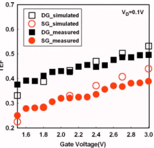
Moreover, due to coupling of the two separate gate biases as the channel body is sufficiently thin, larger barrier lowering with DG operation is confirmed in both experimental and simulated results as shown in Fig. 3. Such barrier lowering results in thermionic emission enhancement. In Fig. 4, ac-cording to Eq.共2兲, the thermionic emission factor,共TEF兲, is defined as,
TEF = exp
冉
− VBkT
冊
. 共3兲The effective TEF can be obtained by substituting the ex-tracted VB into Eq.共3兲. To verify the experimental data with
simulation we employ the following relation:
TEF = 兰0 d n共y兲exp
冋
− qVB共y兲 kT册
dy冕
0 d n共y兲dy , 共4兲where d is the channel thickness, n共y兲 and VB共y兲 are the
simulated electron density and barrier height at depth y, re-spectively. As shown in Fig. 4, the simulated results show
excellent agreement with the trend found experimentally. As compared with the SG operation, more efficient thermionic emission is resulted with the DG operation, owing to the enhancement in barrier lowering as the coupling of the two gate biases occurs.
In this work the physical mechanism responsible for the performance enhancement of poly-Si TFTs with ultrathin channel under DG operation is explored. The experimental data indicate that the DG operation results in additional bar-rier lowering and thus leads to significant improvement in the output drain current as compared with that of the SG operation. Such effect is verified with the simulation results.
This work was supported in part by the National Science Council under Contract No. NSC 96-2221-E-009-212-MY3.
1S. Zhang, C. Zhu, J. K. O. Sin, J. N. Li, and P. K. Mok, IEEE Trans.
Electron Devices 47, 569共2000兲.
2S. Uchikoga, MRS Bull. 27, 881共2002兲.
3A. G. Lewis, I.-W. Wu, T. Y. Huang, A. Chiang, and R. H. Bruce, Tech. Dig. - Int. Electron Devices Meet. 1990, 843.
4H.-C. Lin, C.-J. Su, C.-Y. Hsiao, Y.-S. Yang, and T.-Y. Huang,Appl. Phys.
Lett. 91, 202113共2007兲.
5H.-C. Lin, H.-H. Hsu, C.-J. Su, and T.-Y. Huang,IEEE Electron Device
Lett. 29, 718共2008兲.
6Y. X. Liu, M. Masahara, K. Ishii, T. Sekigawa, H. Takashima, H. Yamau-chi, and E. Suzuki,IEEE Electron Device Lett. 25, 510共2004兲.
7W.-C. Chen, H.-C. Lin, Y.-C. Chang, and T.-Y. Huang,Appl. Phys. Lett.
95, 133502共2009兲.
8F. J. G. Ruiz, A. Godoy, F. Gámiz, C. Sampedro, and L. Donetti,IEEE
Trans. Electron Devices 54,3369共2007兲.
9F. Balestra, S. Cristoloveanu, M. Benachir, J. Brini, and T. Elewa,IEEE
Electron Device Lett. 8, 410共1987兲.
10J. Y. W. Seto,J. Appl. Phys. 46, 5247共1975兲.
11J. Levinson, F. R. Shepherd, P. J. Scanlon, W. D. Westood, G. Este, and M. Rider,J. Appl. Phys. 53, 1193共1982兲.
12B. Faughnan,Appl. Phys. Lett. 50, 290共1987兲.
13ISE TCAD Rel, 10.0 Manual, DESSIS共ISE Integrated Systems Engineer-ing AG, Zurich, 2004兲.
14M. H. Lee, K. H. Chang, and H. C. Lin, J. Appl. Phys. 102, 054508 共2007兲.
15E. Poon and W. Hwang,Solid-State Electron. 25, 699共1982兲.
16W.-C. Chen, Y.-C. Chang, H.-C. Lin, and T.-Y. Huang, Proceedings of the Ext. Abs. Intl. Solid-State Devices and Materials 共SSDM兲, 2009, paper E-7-1.
FIG. 4. 共Color online兲 Comparisons of experimental and simulated TEF under DG and SG operations.
072108-3 Lin et al. Appl. Phys. Lett. 96, 072108共2010兲
This article is copyrighted as indicated in the article. Reuse of AIP content is subject to the terms at: http://scitation.aip.org/termsconditions. Downloaded to IP: 140.113.38.11 On: Wed, 30 Apr 2014 11:58:27