This content has been downloaded from IOPscience. Please scroll down to see the full text.
Download details:
IP Address: 140.113.38.11
This content was downloaded on 25/04/2014 at 02:48
Please note that terms and conditions apply.
Enhanced visible photoluminescence from ultrathin ZnO films grown on Si-nanowires by
atomic layer deposition
View the table of contents for this issue, or go to the journal homepage for more 2010 Nanotechnology 21 385705
(http://iopscience.iop.org/0957-4484/21/38/385705)
Nanotechnology 21 (2010) 385705 (7pp) doi:10.1088/0957-4484/21/38/385705
Enhanced visible photoluminescence from
ultrathin ZnO films grown on
Si-nanowires by atomic layer deposition
Yuan-Ming Chang
1, Sheng-Rui Jian
1,6, Hsin-Yi Lee
2,3,
Chih-Ming Lin
4and Jenh-Yih Juang
51Department of Materials Science and Engineering, I-Shou University, Kaohsiung 840, Taiwan
2National Synchrotron Radiation Research Center, Hsinchu 300, Taiwan
3Department of Materials Science and Engineering, National Chiao Tung University, Hsinchu 300, Taiwan
4Department of Applied Science, National Hsinchu University of Education, Hsinchu 300, Taiwan
5Department of Electrophysics, National Chiao Tung University, Hsinchu 300, Taiwan E-mail:[email protected],[email protected]@g2.nctu.edu.tw
Received 15 June 2010, in final form 16 June 2010 Published 27 August 2010
Online atstacks.iop.org/Nano/21/385705 Abstract
Bright room temperature visible emission is obtained in heterostructures consisting of∼3.5 nm thick ZnO ultrathin films grown on Si-nanowires produced by means of self-masking dry etching in hydrogen-containing plasma. The ZnO films were deposited on Si-nanowires by using atomic layer deposition (ALD) under an ambient temperature of 25◦C. The orders of magnitude enhancement in the intensity of the room temperature photoluminescence peaked around 560 nm in the present ZnO/Si-nanowire heterostructures is presumably due to the high aspect (surface/volume) ratio inherent to the Si-nanowires, which has, in turn, allowed
considerably more ZnO material to be grown on the template and led to markedly more efficient visible emission. Moreover, the ordered nanowire structure also features an extremely low reflectance (∼0.15%) at 325 nm, which may further enhance the efficiency of emission by effectively trapping the excitation light.
(Some figures in this article are in colour only in the electronic version)
1. Introduction
One-dimensional nanostructures, including wires, rods, belts, and tubes, have attracted tremendous research interest over the last decade owing to their wide potential applications [1]. Among them, ZnO-nanowire is regarded as one of the most promising materials for manufacturing a wide variety of high performance devices [2–4]. In particular, the wide bandgap of ∼3.37 eV and large exciton binding energy of ∼60 meV inherent to ZnO have been demonstrated to exhibit efficient excitonic emission at room temperature, making ZnO a promising material for optoelectronic applications. Consequently, considerable efforts have been devoted to this
6 Author to whom any correspondence should be addressed.
particular material in order to harvest efficient ultraviolet luminescence (UVL) from ZnO [5–7]. However, depending on the forms of ZnO specimens and the methods used for preparing them, it is rather common to observe an accompanied broad emission spectrum in the visible regime. From the practical point of view, the presence of the broad visible emission, even though it will inevitably compromise the efficiency of the UVL, will, nevertheless, also offer an alternative for obtaining a visible light source [8].
The origins of the visible emission obtained have been attributed to a variety of ‘intrinsic’ and ‘extrinsic’ factors and remain controversial [9]. For instance, Meng et al [10] reported dramatic effects of annealing temperature on the green luminescence from ZnO nanorods post-annealed in oxygen atmosphere and suggested that such deep-level
Nanotechnology 21 (2010) 385705 Y-M Chang et al related emission results from oxygen vacancies within the
ZnO nanorods. On the other hand, Li et al [4], by applying both chemical and evaporation methods to prepare ZnO thin films, argued that the deep levels involved in the yellow luminescence are likely to be interstitial oxygen while those responsible for green luminescence are primarily surface defects. Shalish et al [11] quantitatively compared the relationship between the defect emission efficiency and the size of ZnO-nanowires and proposed that surface recombination is the primary origin of the deep-level luminescence. They argued that a surface recombination layer with a thickness of about 30 nm may have 100% recombination probability, thus, in quantum-size nanowires, it might entirely quench the band-to-band recombination. It is generally conceived that the photoluminescence characteristics of various ZnO structures are not fundamentally different from those obtained in ZnO thin films and the observed size effects in nanorods and nanowires are more relevant to the surface-to-volume ratio rather than arising from quantum confinement [9].
Based on the above-mentioned understandings about the correlations between the visible emission and type of defects, it appears that ultrathin (<30 nm) ZnO films could be an excellent candidate for obtaining a visible light source with controllable spectrum range provided the defects involved can be engineered through processing conditions. Unfortunately, due to the inherent reflectance and relatively small amount of emissive material involved, the light emission from the planar thin films is often very inefficient with weak intensity, and thus may seriously hinder the possibility of any practical applications. Therefore, it is desirable to develop a viable approach that can harvest defect-related visible luminescence in a more efficient fashion. In this study, we demonstrate that, by growing a layer of ultrathin ZnO film (∼3.5 nm) on the Si-nanowire template, efficient visible light emission can be easily obtained. The high density ZnO/Si-nanowire heterostructure (∼3 × 1012 cm−2) not only has a high surface/volume ratio needed for increasing the area of light emission, but also acts as an excellent anti-reflection layer.
2. Experimental details
The wafer-scale production of Si-nanowires was carried out in an inductively coupled plasma chemical vapor deposition (ICPCVD) system with the following processes. Prior to performing the etching processes, CF4 and O2 plasma were
applied to clean the chamber. After the Si(100) wafer was loaded into the reactive chamber, it was pumped to a pressure of 5× 10⁻⁵ Torr with the substrate holder being heated to 400◦C. Subsequently, the H2gas with a flow rate of 160 sccm
was introduced into the reactor with the pressure being kept at 30 mTorr. The etching process was operated with the radio-frequency (RF) and dc-bias power being maintained at 550 W and 280 W, respectively. Details of the processes and the possible mechanisms involved in obtaining Si-nanowires with the H2-plasma etching were described and discussed
previously [12–16]. However, in order to obtain Si-nanowires with higher aspect ratio, we have increased the duration of H2
-plasma etching to 90 min in this study. The field emission
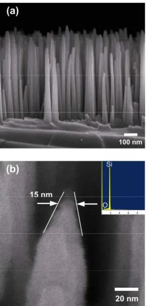
Figure 1. The FESEM images for (a) the cross-sectional (side-view)
and (b) the close-up view of the tip of the Si-nanowire template. The inset shows the EDS analysis of the nanowires, indicating that the predominant composition is Si.
scanning electron microscope (FESEM) image shown in figure1(a) displays the typical morphology of the Si-nanowires obtained by the present process. As is evident from the SEM image, the Si-nanowires are about 1 μm in height and are aligned vertically with an average diameter of about 40–60 nm and a density of∼3 × 1012 cm−2. Moreover, as shown in figure 1(b), the close-up image indicates that the diameter of the nanowire tip is only about 15 nm with evidence of it being slightly oxidized (see the inset of figure1(b)). It has been pointed out that both the physical bombardment of the energetic ions and chemical etching in the reduced H2 plasma
play an essential role for the formation of these vertically aligned Si-nanowires. In this regard, it is quite remarkable that such a simple single-step procedure can yield well-aligned Si-nanowires over a large surface area.
Ultrathin ZnO films were deposited onto these nanowire-covered Si substrates at an ambient temperature of∼25◦C by atomic layer deposition (ALD). ALD is a growth technique 2
that employs a self-limiting vapor-phase chemisorption which depends on consecutive surface reactions. In particular, it applies critical purge steps to prevent interactions between reactive precursors [12]. Briefly, the pulse durations of water and diethylzinc (DEZn) were 100 ms and 50 ms, respectively. The stock time for both water and DEZn was set to 15 s in the stock mode. The purge and pumping periods were 15 s and N2 was used as the purge gas with the pressure being set to
5× 10⁻² Torr. In this way, the films are essentially growing in a monolayer-by-monolayer growth fashion. Previously, it was demonstrated that ZnO films with very smooth surface could be obtained by incorporating the ALD processes with an interrupted flow [13]. In this work, similar procedures were used for depositing ultrathin ZnO films on the surface of Si-nanowires and the thicknesses of the ZnO thin films were estimated to be about 3.5 nm and 15 nm for films grown with 10 and 40 ALD cycles, respectively. As will be described later in the experimental results, the intensity of both the visible and band-edge emissions from the present ZnO/Si-nanowire heterostructures can be significantly enhanced as compared to those from the ultrathin ZnO films deposited on the polished Si(100) substrates and Si-nanowire arrays with similar deposition conditions [13,17].
The crystallographic structure and the phases formed in the ZnO/Si-nanowire heterostructures were characterized by measuring the grazing incidence x-ray diffraction with a synchrotron x-ray source. The synchrotron x-ray experiments were performed at wiggler beamline BL-17B1 at the National Synchrotron Radiation Research Center (NSRRC), Hsinchu, Taiwan. The incident x-ray was focused vertically with a mirror and turned into an 8 keV monochromatic x-ray by using a Si(111) double-crystal monochromator. A FESEM (JEOL JSM-6700F Japan) was used to examine the morphology of the Si-nanowires. Transmission electron microscopy (TEM, JEOL JEM-2010F Japan) with an operating voltage of 200 kV and energy dispersive x-ray spectroscopy (EDS) was used to examine the microstructure and composition of the obtained samples. The photoluminescence (PL) measurements were carried out at room temperature using a He–Cd laser (325 nm, IK3252R-E, Kimmon) for excitation and a CCD (80 K, Spec-10, Princeton Instruments) with a monochromator (0.5 m, SP-2558A, Acton) for detection. The effective wavelength resolution of the PL spectrum was 0.02 nm. Finally, the reflectance of ZnO ultrathin films grown on polished Si and Si-nanowires was measured by the n&k 1200 analyzer (1280 model) with unpolarized light at an incident angle of 4◦. The wavelength range of incident light was from 190 to 1000 nm (deep ultraviolet (DUV) to infrared (IR)).
3. Results and discussion
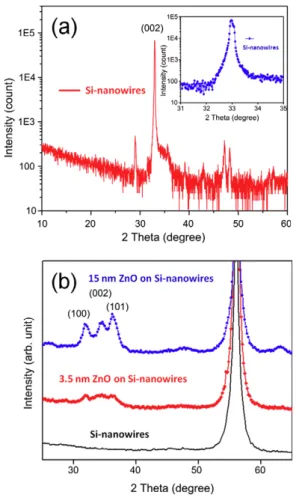
Figure2(a) displays the typicalθ–2θ x-ray diffraction (XRD) results for the plasma-etched Si-nanowires. It is evident that the Si-nanowires obtained by the present H2 plasma etching
method are predominantly (001)-oriented and still have very good crystalline quality. The inset figure 2(a) indicates that the full-width at half-maximum of the (002) diffraction peak is less than 0.1◦. Notice that there are some extra diffraction
Figure 2. (a) The typicalθ–2θ XRD pattern of the Si-nanowires,
indicating the excellent crystallinity of the Si-nanowires even after significant ion bombardments during the plasma etching processes. (b) The grazing incidenceθ–2θ XRD results for bare Si-nanowires as well as for ZnO/Si-nanowire heterostructures with 3.5 and 15 nm thick ZnO layers on Si-nanowires, respectively.
peaks appearing in theθ–2θ scan, presumably originating from other crystallographic planes exposed due to the formation of nanowires. In any case, the results ensure that the subsequent growth of ZnO films is on templates with similar crystalline quality to the pristine Si substrates.
In order to examine the very thin layer of ZnO deposited on the Si-nanowire substrates, the grazing incidence XRD technique was used. Figure 2(b) shows the XRD patterns obtained for the bare Si-nanowire substrate and ZnO films with thicknesses of 3.5 and 15 nm on Si-nanowires, respectively. As compared to the curve obtained for the bare Si-nanowire substrate, it is evident that, for the 15 nm thick ZnO film deposited on Si-nanowires, there are three distinctive diffraction peaks appearing in the 2θ ∼ 30◦–40◦ range, indicating the formation of crystalline ZnO, albeit that the diffraction peaks are weak and rather broadened. On the other hand, for the 3.5 nm thick ZnO film, the peaks in the same range of diffraction angles are much weaker in intensity and are no longer distinguishable, indicating that the ultrathin ZnO films deposited on the Si-nanowire substrate are probably largely amorphous.
To further confirm the structural information suggested by the XRD results for the obtained ZnO films in more
Nanotechnology 21 (2010) 385705 Y-M Chang et al
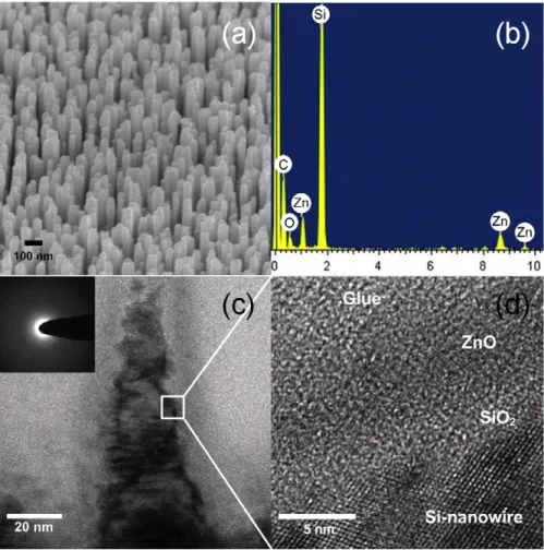
Figure 3. The structural and compositional analyses of the (3.5 nm) ZnO/Si-nanowire heterostructure. (a) The SEM image; (b) the EDS
analysis; (c) the TEM image; and (d) the HRTEM. Notice that the entire layer of the ZnO film is essentially amorphous.
detail, we examined the ZnO/Si-nanowire heterostructures by high resolution transmission electron microscopy (HRTEM). Figure 3(a) shows the typical top-view FESEM image of the ZnO/Si-nanowire heterostructures. It is clear that, as compared with the as-prepared Si-nanowires displayed in figure1, the morphology of the vertically aligned Si-nanowires remains essentially intact after the depositing the ZnO films by ALD processes. The EDS spectrum displayed in figure 3(b) for the 3.5 nm thick ZnO/Si-nanowire sample does reveal the existence of thin ZnO layers on Si-nanowires. The TEM image of one of the Si-nanowire tips which is presumably coated with a layer of 3.5 nm thick ZnO film is displayed in figure3(c). The image appears to exhibit a darker layer throughout the surface of the nanowire tip, indicating that the ALD process does indeed produce rather uniform film deposition even when the thickness is only as thin as 3.5 nm. The insets of figures3(c) and (d) display the selected area diffraction (SAD) pattern and HRTEM image for the area marked by the small square shown in figure3(c), respectively. These images give us a closer look at the interface of ZnO/Si-nanowire heterostructures. It can be seen that the 3.5 nm thick ZnO layer is uniformly deposited on the Si-nanowires and both the SAD pattern and the HRTEM image confirm that the ZnO layer in this case is amorphous, which is also consistent with the XRD results shown in figure2(b). Similar analyses have also been performed for the
Figure 4. The HRTEM image taken from the interface of the
(15 nm) ZnO/Si-nanowire heterostructure. The area in the dashed circle indicates the appearance of ZnO nano-crystallites.
15 nm thick ZnO films deposited on the Si-nanowires under the same ALD conditions. As shown in figure4, in this case, except for the increased thickness, there are regions showing the existence of ZnO nano-crystals within the ZnO layers (see, 4
Figure 5. The room temperature PL spectra obtained for the bare
Si-nanowires, ZnO thin films grown on polished Si, and ZnO/Si-nanowire heterostructures. Notice the emission covers virtually the entire visible spectrum range. The insets (a) and (b) show the bright luminescence taken from 3.5 and 15 nm thick ZnO/Si-nanowire heterostructures, respectively. The photographs clearly show that the luminescence shifts from greenish to yellowish with increasing thickness of ZnO layer.
for example, the area marked by the dashed circle in figure4). This result is, in fact, also in good agreement with the XRD results shown in figure2(b), where distinctive diffraction peaks corresponding to ZnO crystalline phase are observed. Finally, it is noted that both figures3(d) and4also evidently show the high crystalline quality of the Si-nanowires.
After the detailed analyses on the phases and microstruc-tures of the rather defective ZnO films obtained by the present experimental scheme, it is interesting to compare how they behave in the PL characteristics. Figure5displays the room temperature PL spectra obtained from the bare Si-nanowires (i.e. the template used in the present study), the ultrathin ZnO films grown on polished Si and Si-nanowires, respectively. It is noted that there is a very sharp peak at 650 nm in each PL spectrum, which is presumably due to the second harmonic of the 325 nm excitation UV light. In addition, it is also evident that the PL intensity for the bare Si-nanowires is undetectable in the wavelength ranging from 350 to 700 nm, namely the entire visible regime. On the other hand, when ZnO is present, the PL spectrum exhibits a broadened peak covering essentially the entire visible regime, albeit that the intensity of each case is strongly dependent on where and how much the ZnO has been put onto the substrates. This indicates that whatever the detailed mechanism might be the observed visible PL emission must have originated from the ZnO films. In this respect, it should be interesting to compare the spectra corresponding to the three different ZnO films and discuss the implications.
We first compare the two 3.5 nm thick ZnO films deposited under exactly the same conditions but on different Si substrates. As can be seen from the results, except for the intensities, the two spectra display essentially the same PL emission characteristics, namely a broadened spectrum covering the entire visible region and peaking around 560 nm. Indeed, the picture taken by digital camera, as shown in
inset (a) of figure5, evidently displays the greenish glow in the regions exposed to the exciting UV light. It is noted, however, that the ZnO/Si-nanowire heterostructure has a much brighter emission than the ZnO/Si-substrate counterpart. The possible reasons for this difference will be discussed after we compare the results obtained from the 3.5 nm thick and 15 nm thick ZnO/Si-nanowire heterostructures. For the latter, in addition to the observation that the PL emission intensity is further enhanced by increasing the thickness of the ZnO layer, there are two more features worth mentioning. The first is that the peak position of the broadened visible PL emission appears to shift to longer wavelength by about 20 nm. As a result, the emission becomes more yellowish, as displayed in the picture taken by digital camera shown in inset (b) of figure5(a). Moreover, there appears a peak at 369 nm (or 3.36 eV), presumably due to the band-edge emission (∼3.37 eV) resulting from direct electron–hole pair recombination across the intrinsic gap of ZnO. We note here that this is indeed consistent with the microstructure observations described above (figure4), where the appearance of ZnO nano-crystallites is evidently demonstrated for the 15 nm thick films.
As has been mentioned above, the visible PL emissions observed in various ZnO structures have been the subject of extensive research [1–11,18,19] and it is generally conceived that the green PL emission in ZnO is primarily due to oxygen-related defects residing near the surface [10, 11], while the yellow emission is likely related to the deep levels associated with oxygen interstitials [4] and thus is more of a bulk characteristic. However, very recently Tay et al [20] reported two types of green emission, namely the high energy (peak value of 2.465 eV) and low energy (peak value of 2.294 eV) in ZnO powders subjected to different treatments. They have further identified that the former is primarily due to defect-induced surface modification, which in turn gives rise to downwards bad bending through a binding energy shift of the Zn 2p3/2 orbital, while the latter is mostly dominated by
the oxygen vacancies distributed beneath the surface to within the absorption depth (∼70 nm) of the 325 nm He–Cd laser. A closer comparison of the detailed shapes of the spectra also reveals that, unlike the visible PL emission reported in the literature where an apparent emission peak can be easily identified, the spectra obtained in the present study are all much more broadened and cover essentially the whole range of visible light. Since the thickness of the ZnO films studied here (3.5 and 15 nm) is much smaller than the absorption depth of the He–Cd excitation laser, we might think that the PL emissions observed in the present study involve the entire layer of ZnO films. Furthermore, as revealed in the HRTEM images displayed in figures3and4, these room-temperature-deposited ZnO films are mostly amorphous and the defects should have some kind of distribution as a function of film thickness. Considering that, although the XRD results show that the Si-nanowires are of very good crystallinity, it is inevitable that the ion bombardments during plasma etching may have induced a certain degree of damage at the surface of the Si-nanowires [21] and resulted in very defective ZnO layers, especially when the ALD processes were performed at the
Nanotechnology 21 (2010) 385705 Y-M Chang et al
Figure 6. The reflectance curves of ultrathin ZnO films grown on
polished Si (dashed curve) and Si-nanowire arrays (solid curve). Notice the significant differences in reflectance for the two different microstructures.
ambient temperature. Thus, although it is almost impossible to distinguish the surface defects from the bulk ones, the distributions of these defects, nevertheless, are still considered to be responsible for the shifting of the greenish emission seen in the 3.5 nm thick films to the yellowish emission seen in the 15 nm thick films.
Finally, we turn to discuss the apparent enhancement of PL emission exhibited by the ZnO/Si-nanowire heterostructures. As has been mentioned above, although figure 5 evidently demonstrates that the emission from ultrathin ZnO film grown on polished Si is orders of magnitude weaker than that obtained from the ZnO/Si-nanowire heterostructures, the characteristics of the PL emission spectra for ZnO films with the same thickness are very much alike, indicating that they might arise from the same origins. Furthermore, it appears that the emission intensity is further enhanced with increasing film thickness, suggesting that the amount of ZnO existing in the structure might be an essential factor. In this respect, the increased aspect ratio of the template with Si-nanowires [22] could have provided the much needed surface area for depositing extra ZnO with the low-temperature ALD processes. Alternatively, the ZnO/Si-nanowire heterostructures are also found to exhibit excellent anti-reflection capability. As shown in figure 6, the average reflectance of ZnO/Si-nanowire heterostructures is as low as 0.92% for wavelength ranging from 190 to 1000 nm (i.e. DUV to IR). On the other hand, the dashed curve displayed in figure 6 shows that the average reflectance for the ZnO on polished Si-substrate is well over 40% within the same wavelength range. In particular, the reflectance at 325 nm for the ZnO/Si-nanowire heterostructures is less than 0.15% as compared to near 60% for ZnO on polished Si substrates. Furthermore, since the spacing between the ZnO/Si-nanowire heterostructures is much smaller than the wavelength of the incident excitation light, significant reduction in diffraction loss is also anticipated [23]. Both effects might also make significant contributions to the marked enhancement of the observed visible PL emissions. In any case, the present results
appear to indicate an effective alternative route of obtaining full-spectrum visible light emissions by depositing ZnO films onto Si-nanowire templates with controlled thickness.
4. Conclusions
In summary, we have successfully demonstrated the feasibility of utilizing a novel ZnO/Si-nanowire heterostructure to obtain highly efficient room temperature PL emission in the visible range. The structural and optical properties of the ZnO/Si-nanowire heterostructures, as revealed by using FESEM, HRTEM and PL analyses, indicate that the observed visible emissions are intimately related to the highly defective amorphous ZnO layers deposited by ALD processes. Both the increased surface area resulting from the enhanced structural aspect ratio and the anti-reflective characteristics inherent to the nanowire structure are believed to be responsible for the orders of magnitude enhancement in emission intensity reported in the present study.
Acknowledgments
This work was partially supported by the National Science Council of Taiwan under grant Nos: NSC 97-2112-M-214-002-MY2 and NSC 98-2221-E-213-002. JYJ is supported in part by the National Science Council of Taiwan and the MOE-ATP program operated at NCTU. The authors would also like to thank Yan-Chen Chen, Hung-Min Chen and Chih-Ming Wu for useful discussions, Chiung-Chih Hsu for TEM and Mei-Yi Liao for spectrophotometry in the National Nano Device Laboratories (NDL).
References
[1] Xia Y, Yang P, Sun Y, Wu Y, Mayers B, Gates B, Yin Y, Kim F and Yan H 2003 Adv. Mater.15 353
[2] Wang X, Zhou J, Song J, Liu J, Xu N and Wang Z L 2006 Nano Lett.12 2768
[3] Keem K, Jeong D Y and Kim S 2006 Nano Lett.6 1454
[4] Kind H, Yan H, Messer B, Law M and Yang P 2002 Adv. Mater.
14 158
[5] Huang M H, Mao S, Feick H, Yan H, Wu Y, Kind H, Weber E, Russo R and Yang P 2001 Science292 1897
[6] Liu C, Zapien J A, Yao Y, Meng X, Lee C S, Fan S, Lifshitz Y and Lee S T 2003 Adv. Mater.15 838
[7] Mitra A and Thareja R K 2001 J. Appl. Phys.89 2025
[8] Lin Y R, Yang S S, Tsai S Y, Hsu H C, Wu S T and Chen I C 2006 Cryst. Growth Des.6 1951
[9] Djurisic A B and Leung Y H 2006 Small2 944
[10] Meng X Q, Shen D Z, Zhang J Y, Zhao D X, Lu Y M, Dong L, Zhang Z Z, Liu Y C and Fan X W 2005 Solid State Commun.135 179
[11] Shalish I, Temkin H and Narayanamurti V 2004 Phys. Rev. B
69 245401
[12] Ku C S, Huang J M, Lin C M and Lee H Y 2009 Thin Solid Films518 1373
[13] Shieh J, Lin C H and Yang M C 2007 J. Phys. D: Appl. Phys.
40 2242
[14] Yang M C, Shieh J, Hsu C C and Cheng T C 2005 Electrochem. Solid State Lett.8 C131
[15] Scharrer M, Wu X, Yamilov A, Cao H and Chang R P H 2005 Appl. Phys. Lett.86 151113
[16] Shieh J, Hou F J, Chen Y C, Chen H M, Yang S P, Cheng C C and Chen H L 2010 Adv. Mater.22 597
[17] Knez M, Nielsch K and Niinisto L 2007 Adv. Mater.19 3425
[18] Greene L E, Law M, Goldberger J, Kim F, Johnson J C, Zhang Y, Saykally R J and Yang P 2003 Angew. Chem. Int. Edn42 3031
[19] van Dijken A, Meulenkamp E A, Vanmaekelbergh D and Meijerink A 2009 J. Lumin.90 123
[20] Tay Y Y, Tan T T, Boey F, Liang M H, Ye J, Zhao Y, Norby T and Li S 2010 Phys. Chem. Chem. Phys.12 2373
[21] Chen C W, Chen K H, Shen C H, Ganguly A, Chen L C, Wu J J, Wen H I and Pong W F 2006 Appl. Phys. Lett.
88 241905
[22] Garces N Y, Wang L, Bai L, Giles N C, Halliburton L E and Cantwell G 2002 Appl. Phys. Lett.81 622