512 IEEE ELECTRON DEVICE LETTERS, VOL. 17, NO. 12, DECEMBER 1996
A
High-Performance Thi
with a Vertical
Chun-Yen Chang, Fellow, IEEE, and Chiung-Wei Lin
Abstract-In this study, we propose a novel device structure combined with conventional hydrogenated amorphous silicon (a-Si:H) for the source and drain regions and microcrystalline sili- con (pc-Si:H) for the channel region to obtain a high-performance thin-film transistor (TFT). This is a vertical a-Si:H offset struc- ture used to suppress OFF-state current to a small value which is comparable to the conventional a-Si:H 'EFT'S with a much higher drivability. The fabrication process is simple, low temperature (5 300 "C), and low cost, with a potential for high reliability.
I. INTRODUCTION
ECENTLY, hydrogenated amorphous-silicon thin-film
R
transistors (a-Si:H TFT's) have been investigated exten- sively for applications in large area switching devices such as active-matrix liquid crystal display (AM-LCD) [l], [2]. The most serious problems of present a-Si:H TFT's are the low field-effect mobility of carriers in the a-Si:H channel and the reliability. Thus the current driving capability is low. On the other hand, polysilicon (poly-Si) TFT's improve the current drivability while sacrificing the turn-off capability. Hence, there are many investigations for improving the turn- on characteristics of TFT' s including double gate electrode [3], short channel device [4], and vertical structure [SI. For the improvement of drivability of poly-Si TFT's, an offset structure is proposed to reduce the OFF-current [6]. All of these technologies are complicated and costly. Meanwhile, a new crystalline material of higher band mobility (namely microcrystalline silicon, or pc-Si:H) is used to achieve high- speed TFT's 171-[9]. Tsai et al. [lo] proposed an Hz-dilution method to deposit a high-quality pc-Si film which is used in the pc-Si TFT's. Although a higher mobility than a-Si:H TFT's can be obtained, the OFF-currents of pc-Si:H TFT's are still very high; therefore, the ON/OFF current ratio is only five orders of magnitude or less. An offset structure is usually used to suppress the carrier conduction effectively due to the carrier trapping. In this letter, we propose a novel structure the channel of which is composed of pc-Si:H film while intrinsic a-Si:H film is an offset layer to improve the performance. The high conductance of the thin pc-Si:H layer can increase the ON-current and field-effect mobility and the vertical a-Si:H layer suppresses the OFF-current comparable to the conventional a-Si:H device.Manuscript received May 14, 1996; revised August 26, 1996. This work was supported by the National Science Council, R.O.C., under Contract NSC85- The authors are with the Institute of Electronics, National Chiao-Tung Publisher Item Identifier S 0741-3 106(96)08863-5.
22 15-E009-03 8.
University, Hsinchu 300, Taiwan, R.O.C.
0741-3 106/96$05
+
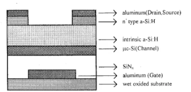
aluininuin(Drain.Source)+
n typea-Si H+
intrinsic a 4 1 H---+
p S i ( C h a n n e l ) aluininuin (Gate) wet oxided substrateFig. 1. device.
A schematic diagram of the proposed novel thin-film transistor
11. EXPERIMENTAL
Our novel device is shown schematically in Fig. 1. The fabrication process is similar to the conventional inverted stagger a-Si:H TFT's except for the insertion of a thin H2- dilution deposited pc-Si:H film embedded between the gate insulator and undoped a-Si:H films. First, an aluminum film 250-nm thick is evaporated on a thermal oxide coated wafer and patterned to form the gate electrode by photolithography and wet etching. Secondly, silicon nitride, H2-diluted pc-Si:H, undoped a-Si:H and n+ a-Si:H films of 300-nm, 20-nm, 140-nm, and 70-nm thicknesses are deposited consecutively in a plasma enhanced chemical vapor deposition (PECVD) system without breaking the vacuum. The silicon nitride film is deposited at 300 "C, 27.78 mw/cm2, 1 torr, while undoped and n+ a-Si:H films are deposited at 250 O C , 25 mw/cm2, 0.3 torr. Besides, pc-Si:H films are deposited at 250 "C, 0.55 torr, and 25 mw/cm2 using the [Hz]/{ [SiH4] +[Hz]} flow
rate ratio values of 980 sccm/(20 sccm
+
980 sccm) for 98% diluted film and 990 sccm/(lO sccm+
990 sccm) for 99% diluted film, respectively. The grain size of pc-Si:H after final processing was approximately 20 nm for 98% diluted film while was 18 nm for the 99% diluted film, respectively. Another aluminum film of 250-nm thickness is also evaporated and patterned to form source-drain electrodes by photolithography and wet etching processes. Finally, we use CF4 plasma etching to define the device active region and remove the unwanted n+ a-Si layer region. All the devices were annealed in 200 "C Nz ambient for 25 min and the electrical properties of our TFT's are measured by a HP4145B semiconductor parameter measurement system with a PC system.111. RESULTS AND DISCUSSIONS
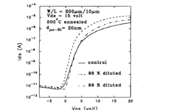
Fig. 2 shows the transfer curves for different devices we made. All the devices have good performances such as small .OO 0 1996 IEEE
CHANG AND LIN: HIGH-PERFORMANCE THIN-FILM TRANSISTOR 513 1 0 - 1 , , , , 7 0 - 5
1
W/L Vds = = 15 2 0 0 ~ m / 1 0 p m volt,A
ZOO°C annealed dl.c-si= ZOnm,,’, ‘ - 5 0 5 1 0 1 5 20 vgs (volt)Fig. 2. Transfer characteristic of the proposed novel thin-film transistor device. Here W is the channel width and L is the channel length for our device.
threshold voltage and sharp transition region. The novel struc- ture devices reveal higher current driving capabilities than the control device (conventional a-Si:H TFT’s). Indeed, we can make sure that our novel device improves turn-on char- acteristics with little degradation due to the a-Si:H. On the other hand, turn-off characteristics will not degrade due to the presence of the a-Si:H layer. The a-Si:H layer behaves like two vertical offset regions to block the carrier conduction in the turn-off state, hence the OFF-current can be suppressed as the control device possesses. As shown in Fig. 2, it is
found that 98% diluted device has a better performance over 99% diluted device. We believe that some ion-bombardment damages due to the Ha-plasma etching effect occur. These damages will produce new trap defects which enhance the trap assisted tunneling [ 111. The large amount of Hz dilution will increase the probability of trap defect formation. Hence, the 99% diluted device shows a smaller ON-current than 98% diluted one. In Fig. 2 and Fig. 3(a), the ONIOFF increases from 7 x l o 5 (0% diluted device) to 5.49 x lo6 (98% diluted device) then drops to 3.36 x lo6 (99% diluted device). The highest ON-current density is due to less bulk trap density. We have measured and deduced the density of deep gap states
(Ndeep) according to the equation: Ndeep = CinsS(qkt)-’
decreases from 4.11 x 10” ern-’ ev-’ (0% dilution) to 2.54 x 10” em-’ ev-’ (98% dilution) then increases to 2.87 x 10” ern-’ ev-’ (99% dilution), where S is the subthreshold swing. From 0% to 98% Hz-plasma, the an- nealing effect prevails which fills the dangling bonds in the amorphous film. Then plasma damage occurs beyond 98% to 99% which produces more bulk trap density. This trend of trapped charge occurs simultaneously in the dielectric film. However, the interface trap is monotonically improved by H2-plasma. The large amount of H2 gas fills the growth ambient such that the growth rate for pc-Si:H is very slow. This produces a smooth interface between gate insulator and pc-Si:H. The 98% diluted device has a smaller threshold voltage of 0.74 V, due to less trapped charges, than 1.19 V for the 99% diluted one. In Fig. 3(b), the conductance of 98% diluted pc-Si:H film is superior to 99% diluted pc- Si:H film such that 98% Hz diluted device has a higher field-effect mobility of 1.87 cm2/v . s, presumably due to less interface state scattering, than 99% diluted device of
1.8 -
-
4- - 0 m OI 0 1.4 - 0 > $ 1 . 6 - - 1 . 2 - 2 2 +. 0 . 8 - 0 r m 1.0 - .c 0 . 6 ’ ’ ’ ’ ’ ’ ’ I 10‘ -20 0 20 4 0 60 80 1 0 0 1 2 0 1.0 m 0.95
.., OI c 2 2 0 . 8 e n 0 c m 5 0.7 v) 0 . 6 H e dilution percentage (%) (a) 0 2 0 4 0 60 8 0 100 H, dilution p e r c e n t a g e (%) (b) 2 . 0-
\ Y N5
v 1.5-
- n E 4- 1.0 8 L 0 2 L 3.5 IFig. 3. The dependence of H2-dilution percentage on (a) threshold voltage, ON/OFF current ratio and (b) subthreshold swing, field-effect mobility of the proposed thin-film transistor device.
1.80 cmz/v. s which are measured in the saturated region and deduced from the equation: I d s = pl.feCinsW(V,,-Vth)’/2L.
The subthreshold swing is also relative to the interface state. The smallest subthreshold swing value of 0.70 Vldec occurs on 98% diluted device which is less than that for the 99% diluted device of 0.75 Vldec. In conclusion, we have made the novel structure devices which demonstrate high performance over the conventional a-Si:H TFT’s. The 20-nm thick pc-Si:H in our device operates well so far. It maybe further improved by optimizing the pc-Si:H thickness in the future.
IV. CONCLUSION
We have proposed a novel vertical offset structure device for the first time to improve the thin-film transistor performance.
A thin Ha-diluted pc-Si:H film is used to increase the turn-on driving current which can enhance operation speed while the vertical a-Si:H offset structure can suppress the OFF-current.
ACKNOWLEDGMENT
The authors would like to thank Dr. T. Y. Huang for his stimulating discussions.
REFERENCES
[ l ] N. Ibaraki, “Technical issues for 40-inch a-Si:H TFT,” in AM-LCD’95
Dig., Japan, 1995, pp. 67-70.
[2] Y. Tsuji, M. Ikeda, Y. Ogawa, and K. Suzuki, “Low resistance MO-W gate linematerial for a-Si:H TFT-LCD’s,” in AM-LCD’95 Dig., Japan,
514 IEEE ELECTRON DEVICE LETTERS, VOL. 17, NO. 12, DECEMBER 1996 [3] Y. Kaneko, K. Tsutsui, H. Matsumaru, H. Yamamoto, and T. Tsukada,
“Amorphorus silicon thin film transistor with a buried double-gate structure,” in IEDM Tech. Dig., 1989, pp. 337-340.
[4] Y. Uchida and M. Matsumura, “Short channel a-Si:H thin-film MOS transistor,” IEEE Trans. Electron Devices, vol. ED-36, pp. 2940-2943, 1984.
[ 5 ] Y. Uchida, Y. Nara, and M. Matsumura, “Proposed vertical-type amorphous-silicon field-effect transistor,” ZEEE Electron Device Lett., vol. EDL-5, pp. 105-107, 1984.
[6] T. Y. Huang, 1. W. Wu, A. G. Lewis, A. Chiang, and R. H. Bruce, “A simple 100-V polysilicon TFT with improved turn-on characteristics,” ZEEE EZectron Device Lett., vol. 11, pp. 244-246, 1990.
[7] S. S . He and G. Lucovsky, “A low temperature plasma-assisted deposi- tion process for microcrystalline thin film transistor, TFT’s,” in Muter. Res. Symp. Proc., 1994, vol. 336, pp. 25-30.
[8] K. C. Hsu, B. Y. Chen, H. T. Hsu, K. C. Wang, T. R. Yew, and H. L. Hwang, “Thin film transistor made from hydrogenated microcrystalline silicon,” Jpn. J. AppZ. Phys., vol. 33, pp. 639-642, 1994.
[9] C. W. Liang, W. C. Chiang, and M. S. Feng, “Microcrystallinity of undoped amorphous silicon film and its effects on the transfer characteristics of thin-film transistor,” Jpn. J. Appl. Phys., vol. 34, pp. 5943-5948, 1995.
[lo] C. C. Tsai, G. B. Anderson, and R. Thompson, “Growth of amor- phous, microcrystalline, and epitaxial silicon in low temperature plasma deposition,” in Muter. Res. Proc., vol. 192, pp. 475-480, 1990. [ 111 See for example, S. M. Sze, Physics of Semiconductor Devices, 2nd ed.