High responsivity of GaN p - i - n photodiode by using low-temperature interlayer
J. C. Lin, Y. K. Su, S. J. Chang, W. H. Lan, K. C. Huang, W. R. Chen, C. Y. Huang, W. C. Lai, W. J. Lin, and Y. C. Cheng
Citation: Applied Physics Letters 91, 173502 (2007); doi: 10.1063/1.2800813
View online: http://dx.doi.org/10.1063/1.2800813
View Table of Contents: http://scitation.aip.org/content/aip/journal/apl/91/17?ver=pdfcov Published by the AIP Publishing
Articles you may be interested in
GaN nanostructured p - i - n photodiodes
Appl. Phys. Lett. 93, 221104 (2008); 10.1063/1.3041641
High-performance 4H-SiC-based ultraviolet p - i - n photodetector J. Appl. Phys. 102, 024505 (2007); 10.1063/1.2747213
Monte Carlo ray trace simulation for micro-ball-lens-integrated high-speed InGaAs p - i - n photodiodes J. Appl. Phys. 101, 033107 (2007); 10.1063/1.2432484
247 nm solar-blind ultraviolet p - i - n photodetector J. Appl. Phys. 100, 096104 (2006); 10.1063/1.2364049
High frequency response of p - i - n photodiodes analyzed by an analytical model in Fourier space J. Appl. Phys. 96, 3839 (2004); 10.1063/1.1787616
This article is copyrighted as indicated in the article. Reuse of AIP content is subject to the terms at: http://scitation.aip.org/termsconditions. Downloaded to IP: 140.113.38.11 On: Thu, 01 May 2014 00:05:24
High responsivity of GaN p-i-n photodiode by using low-temperature
interlayer
J. C. Lin, Y. K. Su,a兲and S. J. Chang
Institute of Microelectronics and Department of Electrical Engineering, National Cheng Kung University, Tainan, 701 Taiwan, Republic of China
W. H. Lan
Department of Electrical Engineering, National University of Kaohsiung, Kaohsiung, 811 Taiwan, Republic of China
K. C. Huang
Department of Electrophysics, National Chiao Tung University, Hsinchu, 300 Taiwan, Republic of China
W. R. Chen
Department of Electronic Engineering, National Formosa University, Huwei, Taiwan 632, Republic of China
C. Y. Huang and W. C. Lai
Institute of Electro-Optical Science and Engineering, National Cheng Kung University, Tainan, 701 Taiwan, Republic of China
W. J. Lin and Y. C. Cheng
Materials and Electro-Optics Research Division, Chung Shan Institute of Science and Technology, Taoyuan, Taiwan 325, Republic of China
共Received 1 August 2007; accepted 1 October 2007; published online 22 October 2007兲
Gallium nitride p-i-n ultraviolet photodiodes with low-temperature 共LT兲-GaN interlayer have been fabricated. It was found that the dark current of photodiode with LT-GaN interlayer is as small as 143 pA at 5 V reverse bias. It was also found that the responsivity of the photodiode with LT-GaN interlayer can be enhanced at a small electric field共⬃0.4 MV/cm兲 due to the carrier multiplication effect. The UV photocurrent gain of 13 and large ionization coefficient 共␣= 3.1⫻105cm−1兲 were also observed in the detector with LT-GaN interlayer. Furthermore, we can achieve a large peak responsivity of 2.27 A / W from the photodiode with LT-GaN interlayer. © 2007 American Institute
of Physics. 关DOI:10.1063/1.2800813兴
Nitride-based semiconductors have been commercialized on light-emitting diodes1and laser diodes2共LDs兲 due to their excellent optical and electrical properties. On the other hand, the devices based on nitride semiconductors are also suitable as detectors for ultraviolet共UV兲 radiation detection because of their wide direct band gap, high breakdown fields, and high-temperature operation. GaN-based photodiodes have potential applications in chemical sensing, flame and heat detection, and missile detection.3,4 In the past few years, GaN p-i-n photodiodes have been fabricated in different types of structures.5–12In this work, we present the properties of a p-i-n structure which inserts a low-temperature 共LT兲-GaN thin layer in intrinsic absorption layer. It is known that the LT-GaN layer as nucleation layer is necessary to grow high quality GaN epitaxial films.13It is also known that LT-GaN interlayer can suppress threading dislocations extending to the subsequently grown high-temperature共HT兲-GaN epi-taxial layers.14,15The LT-GaN cap layer can also be used to serve as the passivation layer of GaN Schottky diodes.16,17 We applied thin LT-GaN layer as an interlayer in the absorp-tion layer of the GaN p-i-n structures. The electrical and optical properties of the fabricated photodiodes with and without LT-GaN interlayer will also be discussed.
The device structures of this work were all grown on
c-plane共0 0 0 1兲 sapphire substrates by a low-pressure
met-alorganic chemical vapor deposition system.
Trimethylgal-lium 共TMGa兲, trimethylaluminum 共TMAl兲, and ammonia 共NH3兲 were used as the source materials of Ga, Al, and N,
respectively. Silane共SiH4兲 and
bis共cyclopentadienyl兲magne-sium 共Cp2Mg兲 were used as the n-type and p-type dopant
sources. The carrier gases were hydrogen and nitrogen. Prior to the growth, sapphire substrates were first heated to 1120 ° C in a stream of hydrogen to clean up the substrate surfaces. Then a two-step growth procedure was employed with a low-temperature GaN nucleation layer grown at 520 ° C and the high-temperature epitaxial layers grown at 1120 ° C. The p-i-n photodiode structure consists of a 25-nm-thick GaN nucleation layer, a 4-m-thick Si-doped
n-GaN layer, a 1-m-thick undoped GaN absorption layer, a 20-nm-thick Mg-doped p-GaN layer, a Mg-doped Al0.15Ga0.85N / GaN strain layer superlattice共SLS兲 structure,
and a 12-nm-thick delta-doped p-GaN contact layer共sample A兲. The Mg-doped Al0.15Ga0.85N / GaN SLS structure
con-sists of three pairs of 8-nm-thick Al0.15Ga0.85N layers
and 8-nm-thick GaN layers. The purpose of using
p-AlGaN / GaN SLS structure is to achieve a higher hole
concentration and more photon incident at GaN absorption range.18The other p-i-n structure is the same as sample A but inserts a 30-nm-thick LT-GaN layer in the middle of 1-m-thick undoped GaN absorption layer 共sample B兲. All samples were subsequently annealed in situ to active Mg in the p-type layers. GaN p-i-n photodiodes were then fabri-cated by conventional photolithography and inductively coupled plasma etching. Ni–Au contact was subsequently
a兲Electronic mail: [email protected]
APPLIED PHYSICS LETTERS 91, 173502共2007兲
0003-6951/2007/91共17兲/173502/3/$23.00 91, 173502-1 © 2007 American Institute of Physics This article is copyrighted as indicated in the article. Reuse of AIP content is subject to the terms at: http://scitation.aip.org/termsconditions. Downloaded to IP:
evaporated onto the p-type GaN surface to serve as the p electrode. On the other hand, Cr–Pt–Au contact was depos-ited onto the exposed n-type GaN layer to serve as the n electrode. The wafers were then lapped down to 100m and fabricated to the size of 325⫻325m2 chips. After these
procedures, we used a HP-4156B semiconductor parameter analyzer to measure current-voltage共I-V兲 characteristics of the fabricated photodiodes. Spectral responsivity measure-ment was also performed by Jobin Yvon SPEX 1000M Sys-tem with a xenon arc lamp light source. All the optical sys-tems are calibrated by using an UV-enhanced silicon photodiode.
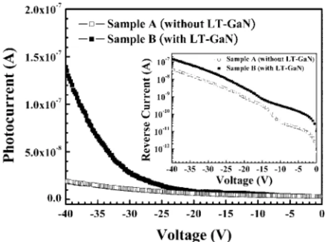
Figure 1 shows a measured photocurrent under xenon light source illumination at room temperature. It can be seen that the photocurrent increased largely after 20 V reverse bias at the sample with LT-GaN interlayer. The increase of photocurrent also shows an internal current gain in sample B. In contrast, the photocurrent of sample A was almost flat in the whole measurement range, as shown in Fig.1. The inset of Fig.1shows the dark currents of the two fabricated pho-todiodes measured at room temperature. The dark currents of sample A at 5 and 40 V reverse biases are 15.7 pA and 36.6 nA, respectively, while the dark currents of sample B at 5 and 40 V reverse biases are 143 pA and 147 nA, respec-tively. The slight increase of dark current in sample B may be attributed to the leakage paths formed from LT-GaN in-terlayer. It can also be seen that the reverse breakdown volt-age of both samples is more than 40 V. Thus, the current gain in sample B can not be attributed to avalanche multipli-cation effect.
Figure2shows the UV photoresponse to excitation with 360 nm light and dark current of sample B. The current gain was also shown in the right axis of Fig.2and determined by using the photocurrent at a bias of 1 V as the unity gain reference point. It was found that the current gain occurred at 20 V reverse bias and reached a value of 13 at 40 V reverse bias 共limited by measurement equipment兲. It is known that the current gain can be obtained through the avalanche mul-tiplication effect in avalanche photodiodes. The avalanche multiplication not only depends on the high electric field but also on the overall spatial distance. Electric fields around 3.5 and 2.8 MV/ cm across the transition region with i-layer thicknesses 100 and 300 nm are necessary for GaN ava-lanche photodiodes to operate at avaava-lanche mode.19,20 This large electric field in the transition region would provide an
electron which was accelerated to high enough kinetic en-ergy共⬎Eg兲 to cause an ionizing collision within the lattice. Such interaction would result in carrier multiplication. Com-paring to these avalanche photodiodes, the thickness of ab-sorption layer of sample B is larger than that of avalanche photodiode. The carrier multiplication would be achieved with a lower estimated electric field at around 0.4 MV/ cm 共with 40 V reverse bias across the 1000 nm i layer兲 by the
p-i-n structure proposed in this work共sample B兲. It was also
known that the crystal quality of LT-GaN layer is not as good as the quality of HT-GaN layer. Then, some defect related trap levels should exist within the band gap of LT-GaN in-terlayer. The bonding energy of defect-trapped carriers should be smaller than the energy of lattices bonding. Thus, less energy is needed to cause the carrier multiplication from these energy levels within the band gap of the LT-GaN inter-layer. The electric field we need in sample B is much smaller than those in other reported GaN avalanche photodiodes.19,20 It is also found that the current gain increased smoothly, which means that no microplasma emissions are observed.19 Figure 3 shows the ionization coefficient of sample B versus applied reverse bias. The ionization coefficient 共␣兲 can be extracted from the following equation by the assump-tion that electron共␣e兲 and hole 共␣h兲 ionizations are the same in GaN共␣e=␣h=␣兲:21 M = 1 1 −
冕
0 L ␣dx ,where M is the multiplication gain, L is the length of multi-plication region, and␣is the ionization coefficient. Since the
FIG. 1. Measured photocurrent of photodiodes with共sample B兲 and without 共sample A兲 LT-GaN interlayer under xenon light illumination. The inset shows the dark I-V characteristics of both samples.
FIG. 2. Reverse I-V characteristics of sample B in the dark and 360 nm light illumination. The right-hand axis indicates the photocurrent gain.
FIG. 3. Ionization coefficient in sample B vs various reverse biases. 173502-2 Lin et al. Appl. Phys. Lett. 91, 173502共2007兲
This article is copyrighted as indicated in the article. Reuse of AIP content is subject to the terms at: http://scitation.aip.org/termsconditions. Downloaded to IP: 140.113.38.11 On: Thu, 01 May 2014 00:05:24
carrier multiplication only happened in the photodiode with LT-GaN interlayer, we can assume that the multiplication region is exactly the LT-GaN interlayer, i.e., L = 30 nm. Thus, the ionization coefficient which can be calculated from the above equation is 3.1⫻105cm−1. This value of ionization
coefficient is larger than those in other reported photodiodes by Carrano et al.19 共␣= 9.6⫻104cm−1兲 and Limb et al.20 共␣= 3.3⫻104cm−1兲. The larger ionization coefficient could
be attributed to the large multiplication carrier generated from the defect-trapped levels in the LT-GaN interlayer. In Fig.3, we also observed the soft ionization at a small reverse bias共⬍20 V兲 and the saturation trend at high reverse bias. The soft ionization may be due to the trap-assisted tunneling mechanism by the defect-trapped levels in the LT-GaN interlayer.22 The saturation trend in ionization coefficient shows the multiplication carrier generated from the interme-diate energy states, not from the valence band.23
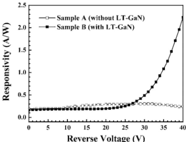
Figure 4 shows the responsivities of samples A and B, which are measured at 360 nm wavelength. A typical respon-sivity of a GaN p-i-n photodiode varied with voltages was observed in sample A. The responsivity increased slightly with increasing applied voltage. The 360 nm wavelength re-sponsivities of the sample A at 0 and 40 V reverse biases are 0.18 and 0.24 A / W, respectively. The slight decrease of re-ponsivity in sample A at high reverse bias共⬎35 V兲 could be attributed to the increasing high dark current. In contrast, the responsivity of sample B increased largely with increasing applied voltage because of the carrier multiplication effect. The 360 nm wavelength responsivities of sample B at 0 and 40 V reverse biases are 0.16 and 2.27 A / W, respectively. In Fig.4, it was also found that the peak responsivity共360 nm兲 of sample B was smaller than that of sample A at a reverse bias of less than 25 V. This may be due to that the photoge-nerated carriers were compensated by the defect levels of LT-GaN interlayer in sample B. On the other hand, the re-sponsivity of sample B was much larger than that of sample A when the applied bias was higher than 25 V reverse bias. This could be attributed to the carrier multiplication effect caused by the same defect levels of LT-GaN interlayer in the sample B. The peak responsivity of sample B was 9.5 times larger than that of the sample A at 40 V reverse bias.
In summary, nitride-based p-i-n UV photodiodes with LT-GaN interlayer have been fabricated. It was found that the dark current of photodiode with LT-GaN interlayer is as
small as 143 pA at 5 V reverse bias. It was also found that the responsivity of the photodiode with LT-GaN interlayer can be enhanced at a small electric field共⬃0.4 MV/cm兲 due to the carrier multiplication effect. The UV photocurrent gain of 13 and large ionization coefficient 共␣= 3.1⫻105cm−1兲
were also observed in the detector with LT-GaN interlayer. Furthermore, we can achieve a large peak responsivity of 2.27 A / W from the photodiode with LT-GaN interlayer. This value of responsivity is 9.5 times larger than the responsivity of the conventional p-i-n GaN photodiode.
The authors would like to acknowledge the support from the Advanced Optoelectronic Technology Center, National Cheng Kung University, the Chung Shan Institute of Science and Technology, and the National Science Council for their research grant共No. NSC96-2221-E-390-013兲.
1S. Nakamura, M. Senoh, N. Iwasa, and S. C. Nagahama, Appl. Phys. Lett.
67, 1868共1995兲.
2S. Nakamura, M. Senoh, S. Nagahama, N. Iwasa, T. Yamada, T. Matsushita, Y. Sugimoto, and H. Kiyoku, Jpn. J. Appl. Phys., Part 2 36, L1059共1997兲.
3A. Hirano, C. Pernot, M. Iwaya, T. Detchprohm, H. Amano, and I. Akasaki, Phys. Status Solidi A 188, 293共2001兲.
4M. Razeghi and A. Rogalski, J. Appl. Phys. 79, 7433共1996兲.
5D. Walker, A. Saxler, P. Kung, X. Zhang, M. Hamilton, J. Diaz, and M. Razeghi, Appl. Phys. Lett. 72, 3303共1998兲.
6G. Y. Xu, A. Salvador, W. Kim, Z. Fan, C. Lu, H. Tang, H. Morkoc, G. Smith, M. Estes, B. Goldenberg, W. Yang, and S. Krishnankutty, Appl. Phys. Lett. 71, 2154共1997兲.
7A. Osinsky, S. Gangopadhyay, R. Gaska, B. Williams, M. A. Khan, D. Kuksenkov, and H. Temkin, Appl. Phys. Lett. 71, 2334共1997兲. 8C. K. Wang, T. K. Ko, C. S. Chang, S. J. Chang, Y. K. Su, T. C. Wen, C.
H. Kuo, and Y. Z. Chiou, IEEE Photonics Technol. Lett. 17, 2161共2005兲. 9S. J. Chang, T. K. Ko, Y. K. Su, Y. Z. Chiou, C. S. Chang, S. C. Shei, J. K. Sheu, W. C. Lai, Y. C. Lin, W. S. Chen, and C. F. Shen, IEEE Sens. J.
6, 406共2006兲.
10T. K. Ko, S. C. Shei, S. J. Chang, Y. K. Su, Y. Z. Chiou, Y. C. Lin, C. S. Chang, W. S. Chen, C. K. Wang, J. K. Sheu, and W. C. Lai, IEEE Sens. J.
6, 964共2006兲.
11Y. C. Cheng, J. C. Lin, and W. J. Lin, Abstracts and Schedule of UK Compound Semiconductors 2006共Abstract Book兲, Paper No. F-O-3 11.45 SBLT02.
12G. Y. Xu, A. Salvador, W. Kim, Z. Fan, C. Lu, H. Tang, H. Morkoc, G. Smith, M. Estes, B. Goldenberg, W. Yang, and S. Krishnankutty, Appl. Phys. Lett. 71, 2154共1997兲.
13S. Nakamura, Jpn. J. Appl. Phys., Part 2 30, L1705共1991兲.
14M. Iwaya, T. Takeuchi, S. Yamaguchi, C. Wetzel, H. Amano, and I. Akasaki, Jpn. J. Appl. Phys., Part 2 37, L316共1998兲.
15E. D. Bourret-Courchesne, S. Kellermann, K. M. Yu, M. Benamara, Z. Liliental-Weber, J. Washburn, S. J. C. Irvine, and A. Stafford, Appl. Phys. Lett. 77, 3562共2000兲.
16S. J. Chang, C. L. Yu, C. H. Chen, P. C. Chang, and K. C. Huang, J. Vac. Sci. Technol. A 24, 637共2006兲.
17M. L. Lee, J. K. Sheu, W. C. Lai, S. J. Chang, Y. K. Su, M. G. Chen, C. J. Kao, G. C. Chi, and J. M. Tsai, Appl. Phys. Lett. 82, 2913共2003兲. 18L. S. Yeh, M. L. Lee, J. K. Sheu, M. G. Chen, C. J. Kao, G. C. Chi, S. J.
Chang, and Y. K. Su, Solid-State Electron. 47, 873共2003兲.
19J. C. Carrano, D. J. H. Lambert, C. J. Eiting, C. J. Collins, T. Li, S. Wang, B. Yang, A. L. Beck, R. D. Dupuis, and J. C. Campbell, Appl. Phys. Lett.
76, 924共2000兲.
20J. B. Limb, D. Yoo, J. H. Ryou, W. Lee, S. C. Shen, R. D. Dupuis, M. L. Reed, C. J. Collins, M. Wraback, D. Hanser, E. Preble, N. M. Williams, and K. Evans, Appl. Phys. Lett. 89, 011112共2006兲.
21M. Trivedi and K. Shenai, J. Appl. Phys. 85, 6889共1999兲.
22J. C. Carrano, T. Li, P. A. Grudowski, C. J. Eiting, R. D. Dupuis, and J. C. Campbell, J. Appl. Phys. 83, 6148共1998兲.
23R. Singh, R. J. Molnar, M. S. Ünlü, and T. D. Moustakas, Appl. Phys. Lett. 64, 336共1994兲.
FIG. 4. Spectral responsivities共360 nm兲 of samples A and B measured at different reverse biases.
173502-3 Lin et al. Appl. Phys. Lett. 91, 173502共2007兲
This article is copyrighted as indicated in the article. Reuse of AIP content is subject to the terms at: http://scitation.aip.org/termsconditions. Downloaded to IP: 140.113.38.11 On: Thu, 01 May 2014 00:05:24