以超高真空化學氣相沉積系統成長低溫複晶矽薄膜
電晶體及其在投影式液晶顯示器的應用— 子計劃一
Fabrication of UHV/CVD low temperature poly-Si TFTs and its
application to projection liquid crystal display
執行期限:89 年 8 月 1 日至 90 年 7 月 31 日
計劃編號:NSC89-2218-E110-018
計劃主持人:中山大學物理研究所 張鼎張副教授
一、中文摘要 本計畫將以三年時間,研究探 討 超 高 真 空 化 學 氣 相 沉 積 系 統 (UHVCVD)沉積之複晶矽及其在 低 溫 複 晶 矽 薄 膜 電 晶 體 上 的 應 用,並嘗試作成小尺寸 UHV/CVD 薄膜電晶體,以配合投影式液晶顯 示器的應用。 第一年將建立超高真空化學 氣相沉積系統沉積複晶矽薄膜電 晶體之資料庫,探討壓力、溫度、 氣體流量及氣體種類等製程因子 的影響。並由 X-ray、TEM、SEM、 AFM 等分析儀器研究複晶矽之晶 格方向、結晶型態、厚度、及表面 平坦度等參數,第二年我們將著重 在低溫複晶矽薄膜電晶的製作,同 時作電性分析,探討不同條件成長 之 UHV/CVD 低溫複晶矽對薄膜 電晶體特性的影響,找出最佳之 UHV/CVD 低 溫 複 晶 矽 沉 積 條 件。最後一年則做小尺寸之低溫 UHV/CVD 薄膜電晶體,探討其短 通道效應,為了更進一步降低製程 溫度及改善薄膜特性,我們也採用 雷射再結晶或雷射退火來製作元 件,並比較這些製程對元件特性及 短通道效應的影響。 關鍵詞:超高真空化學氣相沉積、 小尺寸複晶矽薄膜電晶體、短通道 效應 AbstractThe goal of this project is to investigate the low temperature polycrystalline silicon deposited by ultra high vacuum chemical vapor deposition (UHV/CVD) and its application to polycrystalline silicon thin film transistors in three years. Small dimension UHV/CVD poly-si TFTs will also be fabricated.
In the first year, the database of low temperature polycrystalline silicon deposited by UHV/CVD will be built to investigate the effects of deposition pressure, temperature and gas flow rate. X-ray, TEM, SEM, and AFM will be used to analyze the lattice orientation, film thickness and surface roughness. In the second year, we will focus on the fabrication of low temperature poly-Si TFTs. Typical electrical
characteristics will be analyzed to investigate the influences of UHVCVD low-temperature polycrystalline deposition condition to find the optimal deposition recipe. In the last year, UHV/CVD low temperature poly-Si TFTs with small gate length will be fabricated to study short channel effect. To lower down the process temperature, we also use eximer laser to recrystallize or activate our devices. The influences of these processes on device performance and short channel effects are compared and discussed.
二、緣由與目的
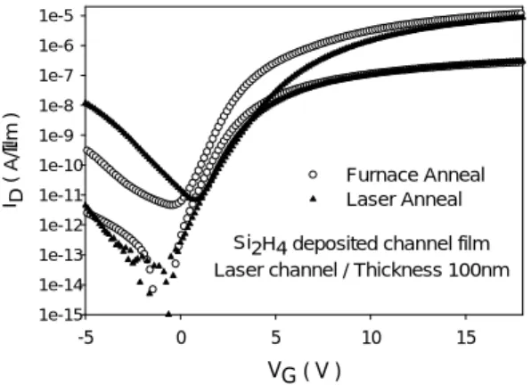
近年來,複晶矽薄膜電晶體在 主 動式 矩 陣 液晶 顯示 器 (Active Matrix Liquid Crystal Display, AMLCD)上的應用越來越受到重 視,因為相較於目前業界所採用的 多晶矽薄膜電晶體,複晶矽薄膜電 晶 體 有 較 高 的 載 子 遷 移 率 (mobility)及較大的導通電流,可以 同時用在製作陣列開關元件以及 週邊驅動電路(driving circuit),使 顯示器和周邊電路整合在同一塊 面板上,大幅降低製程的複雜度及 製作成本[1]。而也由於其遷移率較 高,我們可以縮小電晶體面積,進 而 提 高 液 晶 顯 示 器 的 透 光 率 (aperture ratio),我們甚至可以製作 高密度小尺寸的薄膜電晶體以應 用在投影式電視上。 然而,小尺寸的複晶矽薄膜電 晶體雖然有較高的導通電流和較 佳的次臨界波動特性,卻有著嚴重 的 短 通 道 效 應 。 和 絕 緣 矽 基 板 (SOI,Silicon on Insulator)元件相 似,薄膜電晶體有顯著的浮動基板 效應(Floating Body Effect),在汲極 高電場區域被高能載子撞擊出來 的熱載子會聚集在絕緣的基板而 改變基板電位使得寄生雙極性電 晶體(parasitic BJT)導通,接著大量 電流會由源極進入元件通道,汲極 電流也將呈現非飽和不受極極電 壓 控制 的狀 態, 即所 謂 的 Kink Effect[2]。 根據研究,複晶矽薄膜電晶體 的短通道效應甚至比 SOI 元件更 嚴重,因為其通道內的晶粒結構及 大量聚集在晶粒邊緣的缺陷會增 強載子的衝擊離子化效應(Impact Ionization Effect)[3]。 UHV/CVD 系統是在超高真 空系統下沉積複晶矽薄膜,所以可 以降低薄膜的雜質濃度,如果再配 合雷射使得薄膜再結晶成大晶粒 結構,預期可以得到比雷射再結晶 LPCVD 沉積薄 膜更好的薄 膜品 質,降低晶粒邊界的缺陷密度並從 而抑制小尺寸元件的短通道效應。 三、結果與討論 1. 圖 1.1 是 UHV/CVD 複晶矽薄 膜電晶體的 ID-VD曲線,虛線 表 示 複 晶 矽 薄 膜 是 由 傳 統 SPC(Solid Phase Crystallization) 再結晶而成,實線則表示通道
由準分子雷射再結晶而成。我 們可以明顯看到以雷射再結 晶的元件特性較佳,這是因為 雷射再結晶的複晶矽晶粒較 大,有效缺陷密度較小,所以 元件的遷移率相對較高。但我 們 也 觀 察 到 , 雷 射 再 結 晶 UHV/CVD 薄膜的元件其 kink effect 較明顯、短通道效應較 嚴重,這和襲知 kink effect 會 因缺陷密度降低而被抑制的 現象相牴觸,這可能是因為雷 射再結晶的條件沒有調到最 佳化,使通道底部的晶粒較通 道頂端要小,而浮動基板效應 (Floating Body Effect)會因為 通道底部的缺陷密度增大而 變 嚴 重 , 從 而 增 強 了 kink effect。不過這部分的推論有待 更完善的驗證。 2. 圖 1.2 是比較經過不同活化方 式的元件的 ID-VD特性,我們 發現如果元件使用雷射活化 的方式製作汲極源極時,其導 通電流和用傳統低壓爐管 600 度 24 小時活化的電流差不 多,但是很明顯的其 kink effect 比較嚴重。圖 1.3 則是比較經 過不同活化方式元件的 ID-VG 曲線,發現用雷射活化的元件 其漏電流明顯的增加,而且隨 著閘極電壓的增大而變大。由 於漏電是由汲極端的電場大 小和缺陷密度所影響,所以我 們推論用雷射活化會使汲極 端 和 通 道 間 的 介 面 缺 陷 變 多,從而使得漏電變大而且衝 擊離子化效應增強,kink effect 變嚴重。 3. 圖 1.4 是雷射活化元件的 TEM 照片,可以發現在汲極端和通 道之間的確出現了晶粒結構 較小較亂的區域,這表示當元 件 在 經 過 雷 射 活 化 的 製 程 時,因為通道被閘極覆蓋而不 受雷射影響,汲極源極則被雷 射的高能量融化重新結晶,在 源極/通道的介面處因為溫度 低的通道形同晶種,晶粒會由 通道向汲極/源極方向成長,這 和雷射再結晶時晶粒由融溶 層 底 部 向 上 成 長 的 方 向 不 同;再加上介面也會接收到部 分散射的雷射能量,出現融化 不完全的情形,這使得介面處 會出現結構紛亂小晶粒的區 域,而使漏電變大、kink effect 變嚴重。 四、參考文獻
[1] Jun Koyama, et al., Extended
Abstracts of the 1997
International Conference on solid Stage devices and materials, Hamamatsu, 1997, pp. 348-349
[2] Marina Valdinoci, et al., IEEE Trans. on ED, Vol. 44, No, 12, 1997, pp. 2234-2241.
[3] Noriyoshi Yamauchi, et al., IEEE IEDM 1989, pp. 353-356.
圖 1.1 UHV/CVD 複晶矽薄膜電晶體的
ID-VD曲線。其中實心三角形符號表示元
件通道經過雷射再結晶,空心圓符號則 表示通道為傳統 SPC 再結晶的複晶矽。
Si2H4 deposited channel film Laser channel / Thickness 100nm
VD ( V ) 0 2 4 6 8 10 12 14 I D ( mA ) 0.0 0.2 0.4 0.6 0.8 1.0 Furnace Anneal Laser Anneal 圖 1.2 經過不同方式活化的 UHV/CVD 複晶矽薄膜電晶體的 ID-VD曲線。
Si2H4 deposited channel film Laser channel / Thickness 100nm
VG ( V ) -5 0 5 10 15 I D ( A / µ m ) 1e-15 1e-14 1e-13 1e-12 1e-11 1e-10 1e-9 1e-8 1e-7 1e-6 1e-5 Furnace Anneal Laser Anneal 圖 1.3 經過不同方式活化的 UHV/CVD 複晶矽薄膜電晶體的 ID-VG曲線。 圖 1.4 經過雷射活化的 UHV/CVD 複晶 矽薄膜電晶體的 TEM 照片。 W/L = 50µm/10µm. VD ( V ) 0 2 4 6 8 10 12 14 I D (mA) 0.0 0.2 0.4 0.6 0.8 1.0
Laser annealed channel SPC channel
gate oxide gate
channel