國
立
交
通
大
學
電子工程學系 電子研究所
碩 士 論 文
針對多重臨界電壓 CMOS 設計之
有效率一筆劃電源開關繞線
An Efficient Hamiltonian-Cycle Power-Switch Routing
for MTCMOS Designs
學 生 :王易民
指導教授:趙家佐 博士
國
立
交
通
大
學
電子工程學系 電子研究所
碩 士 論 文
針對多重臨界電壓 CMOS 設計之
有效率一筆劃電源開關繞線
An Efficient Hamiltonian-Cycle Power-Switch Routing
for MTCMOS Designs
學 生 :王易民
指導教授:趙家佐 博士
針對多重臨界電壓 CMOS 設計之
有效率一筆劃電源開關繞線
An Efficient Hamiltonian-Cycle Power-Switch Routing
for MTCMOS Designs
研 究 生:王易民 Student:Yi-Ming Wang
指導教授:趙家佐 Advisor:Chia-Tso Chao
國 立 交 通 大 學
電子工程學系 電子研究所
碩 士 論 文
A ThesisSubmitted to Department of Electronics Engineering and Institute of Electronics
College of Electrical and Computer Engineering National Chiao Tung University
in partial Fulfillment of the Requirements for the Degree of
Master of Science in
Electronics Engineering
August 2012
Hsinchu, Taiwan, Republic of China
i
針對多重臨界電壓CMOS設計之
有效率一筆劃電源開關繞線
學生:王易民
指導教授:趙家佐 博士
國立交通大學 電子工程學系 電子研究所碩士班
摘要
多重臨界電壓 CMOS 因能藉由關掉閒置的電路區域而有效率地減少漏電功耗, 已成為現今業界最常用的電源閘控技術。然而,被電源閘控下的區域在閒置到工 作的模式轉換間可能會消耗大量的瞬間電流。所以主要的 IC 廠商建議一個接著 一個地開啟電源開關以減少模式轉換產生的瞬間電流,故需要漢米爾頓圓環的一 筆劃繞線串連所有的電源開關。本論文提出的電源開關繞線架構可有效率地得到 一條可行的漢米爾頓圓環繞線以連接電源開關,其不違反兩相連電源開關間的曼 哈頓距離限制,同時也能處理因硬體巨集導致電源開關的不規律擺放。此架構可 與商業的自動化流程工具相容且已被設計服務公司用於多重臨界電壓 CMOS 設計 的下線。AN EFFICIENT HAMILTONIAN-CYCLE
POWER-SWITCH ROUTING FOR MTCMOS DESIGNS
Student: Yi-Ming Wang Advisor: Dr. Chia-Tso Chao Department of Electronics Engineering
Istitute of Engineering National Chiao Tung University
Abstract
Multi-threshold CMOS (MTCMOS) is currently the most popular methodol-ogy in industry for implementing a power gating design, which can effectively re-duce the leakage power by turning off inactive circuit domains. However, large peak current may be consumed in a power-gated domain during its sleep-to-active mode transition. As a result, major IC foundries recommend turning on power switches one by one to reduce the peak current during the mode transition, which requires a Hamiltonian-cycle routing to serially connect all the power switches. The pro-posed efficient power-switch routing framework, which can effectively and efficiently find a feasible Hamiltonian-cycle routing among power switches without violating the Manhattan distance constraint between any two power switches while handling the irregular placement of the power switches resulting from the hard macros. The proposed framework is compliant to commercial APR tools and has been used in a major design-service company for taping out complex MTCMOS designs.
Acknowledgements
I would like to express my gratitude to all those who gave me the possibility to complete the dissertation. My sincerest appreciation goes to my advisor, Dr. Mango Chia-Tso Chao, for his guidance in completing this dissertation. A special acknowledgement is forward to professor Shi-Hao Chen and other senior colleagues in Global Unichip Corporation, for their instruction and supported knowledge about tools, experience and the latest research topics from the viewpoint of vendors. The education of professor Hung-Ming Chen and professor Iris Hui-Ru Jiang enrish my backgroud of EDA.
Besides, special thanks for all of the members in my laboratory for these wonderful years. Chen-Wei Lin has given me some experience in realistic working. Wei-Sheng Tu has instructed me in programming. Szu-Pang Mu has discussed some interesting ideas with me; Hao-Yu Yang has taught me many useful skills and background in EDA; Wen-Hsiang Chang, Hao-Wen Hsu, and Chin-Yuan Huang has played basketball and activities with me in leisure time; Chao-Yin Huang and Yu-An Chen has supported me many troublesome works in laboratory.
Next, I want to thank every friends communicating with me during these yeas because your existence enrich my daily life. Dining, chatting, and palying with you released my pressure.
Last but not least, I wish to thank my family for their thoughtful encourage-ment and kind support in my life. Because you raise me up carefully, I can grow up safely and seek my goal in life without physical disturbance.
Yi-Ming Wang National Chiao Tung University
August 2012
Table of Contents
Abstract i
Acknowledgements ii
List of Tables vi
List of Figures vii
Chapter 1. Introduction 1 Chapter 2. Background 5
2.1 Architecture of Power-gating Designs . . . 5
2.2 Power Switch and Switch Routing . . . 5
2.3 Tradeoff of Turning on Power Switches Serially . . . 7
2.4 Manhattan-Distance Constraint . . . 8
Chapter 3. Problem Formulation of Power-switch Routing 10 3.1 Problem Formulation of the Proposed Framework . . . 10
3.2 Power-switch Routing Using a TSP Solver . . . 11
Chapter 4. The Proposed Framework 13 4.1 Cyclic and Acyclic Power-Switch Tour . . . 13
4.2 Data Structure for Power Switch and Hard Macro . . . 13
4.3 Overall Flow . . . 14
4.4 Group Power Switches . . . 15
4.5 Split Overlapping Switch Groups . . . 16
4.6 Tour Switches inside a Group . . . 16 iv
4.6.1 Tour Around-Macro Groups . . . 16
4.6.2 Tour Column-based Groups . . . 17
4.7 Transform Acyclic Sub-tour into Cyclic Ones . . . 17
4.8 Unitization . . . 18
4.9 Merging Operation . . . 19
4.10 Switch Routing with Designated Start and End Points . . . 20 Chapter 5. Experimental Results 22 Chapter 6. Conclusion 26
Bibliography 27
List of Tables
5.1 Routing results of the proposed switch-routing framework on 3 power-gating domains. . . 22 5.2 Simulation results of the proposed switch-routing framework
on 3 power-gating domains. . . 23 5.3 Comparison between the proposed framework and a TSP
solver [22]. . . 25
List of Figures
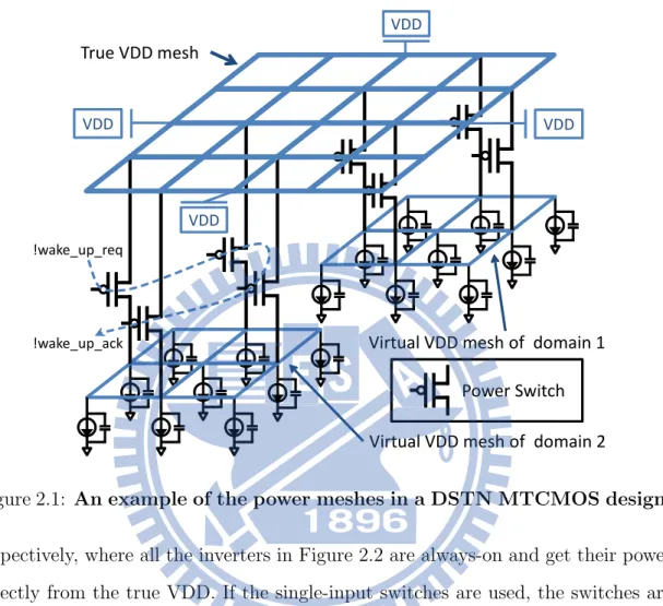
2.1 An example of the power meshes in a DSTN MTCMOS design. 6
2.2 Types of header power switches. . . 7
2.3 Power-switch routing for (a) single-input and (b) double-input switches. . . 7
2.4 The power-up time and peak current of turning on 1 (de-noted as C1), 5 (de(de-noted as C5), and 10 (de(de-noted as C10) power switches at a time. . . 8
4.1 (a) Acyclic and (b) cyclic power-switch tour. . . 13
4.2 The overall algorithm of the proposed switch-routing frame-work. . . 15
4.3 An example of splitting two overlapping groups. . . 16
4.4 Touring switches of combined column-based groups. . . 17
4.5 Transform an acyclic (a) column-based sub-tour or (b) around-macro sub-tour into a cyclic sub-tour by interlacing. . . 18
4.6 The algorithm of unitization. . . 19
4.7 An example of a merging operation. . . 20
4.8 An example of stretching operation. . . 21
Chapter 1
Introduction
The leakage power (static power) of circuits has been greatly increased and gradually dominate an IC’s total power consumption as the process technologies continually scale down [2] [3]. This leakage power consumption may significantly shortened the battery lifetime of electronic products, and hence reducing the leakage power consumption is one of the most critical design tasks for today’s battery-powered portable applications, such as cell phones, tablet PCs, PDAs, and GPS; the market for such applications has been expanding consistently for the past decade and shows no sign of stopping in the foreseeable future. The most straightforward and effective method to reduce leakage power is the power-gating technique, which cuts off the power supply (or ground) of a power-gated domain when idle and resumes the power supply when in operation. As a result, an extremely small leakage power is consumed by the idle power-gated devices.
Being able to simultaneously reduce leakage power for the always-on circuits and maintain performance for the power-gated circuits, the Multi-threshold CMOS (MTCMOS) technology [1] has now become the most popular methodology to realize a power-gating design. In MTCMOS designs, high-Vt transistors are used to build always-on circuits, such as power switches, retention flip-flops, and always-on buffers, such that their leakage power consumption can be further reduced during its idle mode. Meanwhile, low- Vt transistors are used to build the power-gated circuits,
2 such that their perform can still be maintained during its active mode.
Several previous works have been proposed to optimize different design fac-tors for an MTCMOS design. [11] [15] [17] proposed analytical models to minimize the size of switch transistors while satisfying the constraint of the IR drop between true VDD and virtual VDD. [6] [7] [8] [16] [18] minimized the wake-up time by finding
proper turn-on scheduling of power switches while satisfying the constraint of the peak current on the power-gated domain or the worst dynamic IR drop on active domains. [19] [20] introduced new power-switch structure, such as stacking power gating and stepwise switching, to reduce the potential dynamic IR drop on active domain.
In current industrial MTCMOS designs, the distributed sleep transistor net-work (DSTN) [4] is the most popular power-switch structure, where all the power switches share the same mesh of the virtual VDD(or ground) and are connected to the
true VDD in parallel. Compared to the cluster-based switch structure [5] [8] [15] [17],
where one power switch individually supplies one portion of the power-gated cir-cuit, DSTN can result in less IR drop of the power mesh with less area overhead. In TSMC’s reference flow, the power switches in DSTN are recommended to be turned on one by one, instead of in parallel, to reduce the peak current during the sleep-to-active mode transition.
To realize such a serial turn-on sequence, the physical design tools need to find a feasible Hamiltonian-cycle connection among all power switches while the distance between any two adjacent switches must be smaller than a pre-defined Manhattan distance constraint. A connection violating the Manhattan distance constraint may result in a large capacitance which exceeds the characterization range of the timing library, and in turn may generate an unpredictable large delay. In addition, some power switches are placed irregularly due to the existence of hard macro, which
3 further increases the difficulty of finding a feasible Hamiltonian cycle for switch routing. Note that the number of power switches in a power-gated domain can easily exceed 20K in current MTCMOS designs. Such problem space usually exceeds the limit of a general TSP solver [22] [23] [24]. [21] proposed a framework to find a feasible Hamiltonian path (instead of a Hamiltonian cycle) for switch routing, which can only be applied to one type of power switches (double-input power switches) and hence its application is limited. Furthermore, [21] focuses on minimizing the total wire length of switch routing. However, the wire length used for switch routing is only a small portion (usually less than 1%) to the total wire length of the gated circuits. As a result, how to efficiently find a feasible Hamiltonian cycle for switch routing is much more critical than minimize its wire length in practical MTCMOS designs.
In this thesis, we propose a switch-routing framework, which can systemati-cally deal with the irregularity of switches’ placement and efficiently find a feasible Hamiltonian cycle for switch routing. The proposed framework is built compliant to the environment of a commercial APR tool, Encounter [10]. First, the location of power switches and the information of hard macros are extracted from the design data base of Encounter through its Tcl interface. Second, the core of the proposed framework is called from Encounter interface to generate a feasible Hamiltonian cycle for switch routing. Next, the final physical routing of the Hamiltonian-cycle switch routing is realized by Encounter through its Tcl interface. The experiments reported in this thesis are conducted based on 40nm MTCMOS designs. This au-tomatic switch-routing framework is currently used in the MTCMOS design flow of a major design-service company and has successful taped out multiple MTCMOS chips.
4 header switches. The same idea can also be applied to the MTCMOS designs using footer switches easily.
Chapter 2
Background
2.1
Architecture of Power-gating Designs
Figure 2.1 illustrates the power-mesh structure of an exemplary DSTN [4] power-gating design with two power-gated domains. Each power-gated domain uses an independent power mesh to form its own virtual VDD mesh, which supplies power to the circuits in the power-gated domain. A virtual-VDD mesh is connected with the true-VDD mesh through multiple parallel-connected power switches (PMOS transistors) in between. As a result, all the current consumed in a power-gated domain is shared by all the parallel-connected power switches, unlike the cluster-based switch structure [5] [8] [15] [17], where one portion of power-gated circuit is supplied solely by one power switch. The on/off of the power switches are controlled by the wake-up-request signal, which will serially turns on/off the power switches. Once the wake-up-acknowledge signal is received, the system knows whether the gated domain is successfully turned on and then start to send jobs to the gated domain.
2.2
Power Switch and Switch Routing
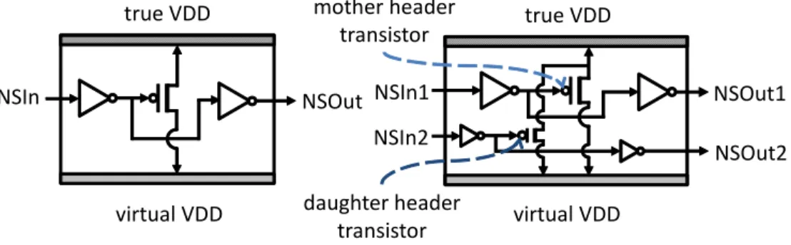
The TSMC library [9] provides two types of header switches: the single-input switches and double-input switches as showed in Figure 2.2(a) and Figure 2.2(b),
6 VDD VDD VDD VDD True VDD mesh
Virtual VDD mesh of domain 2 Virtual VDD mesh of domain 1
Power Switch
!wake_up_req
!wake_up_ack
Figure 2.1: An example of the power meshes in a DSTN MTCMOS design. respectively, where all the inverters in Figure 2.2 are always-on and get their power directly from the true VDD. If the single-input switches are used, the switches are serially connected as Figure 2.3(a), where the NSIn signal of the first routed switch is connected to system’s wake-up-request signal and the NSOut of the last routed switch is connected to the system’s wake-up-acknowledge signal. Since the pins of wake-up-request and wake-up-acknowledge signals usually locate next to each other, the routing of single-input switches will form a Hamiltonian cycle. If the double-input switches are used, the switches are connected as Figure 2.3(b), where the wake-up-request and wake-up-acknowledge signals are connected to the NSIn2 and NSOut1 signals of the first routed switch, respectively. Also, the NSOut2 signal of last routed switch is connected to the NSIn1 signal of itself. Therefore, the routing of double-input switches will form a Hamiltonian path.
7 true VDD true VDD NSIn NSIn1 NSIn2 NSOut NSOut1 NSOut2 virtual VDD virtual VDD mother header transistor daughter header transistor
(a) single input header switch (b) double input header switch Figure 2.2: Types of header power switches.
Figure 2.3: Power-switch routing for (a) single-input and (b) double-input switches.
2.3
Tradeoff of Turning on Power Switches Serially
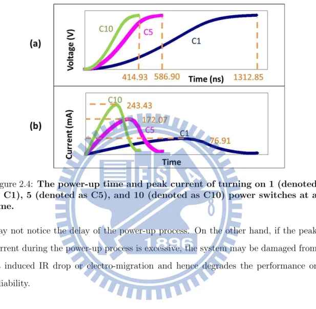
Turning on power switches serially can reduce the peak current during the sleep-to-active mode transition while its power-up time is increased. Figure 2.4(a) and Figure 2.4(b) shows the virtual VDD and the current versus time, respectively, when turning on 1 (denoted by C1), 5 (denoted by C5), and 10 (denoted by C10) power switches at a time. This experiment is performed based on a 40nm power-gated domain with 31559 power switches. As the result shows, the peak current of C1 is significantly lower than that of C5 (44.7%) and C10 (31.6%) while the power-up time of C1 is significantly longer than that of C5 (2.24X) and C10 (3.16X). However, this trade-off is still preferred for most power-gating designs since the system’s transition between power modes does not occur often and the end users
8
Figure 2.4: The power-up time and peak current of turning on 1 (denoted as C1), 5 (denoted as C5), and 10 (denoted as C10) power switches at a time.
may not notice the delay of the power-up process. On the other hand, if the peak current during the power-up process is excessive, the system may be damaged from its induced IR drop or electro-migration and hence degrades the performance or reliability.
2.4
Manhattan-Distance Constraint
When connecting two power switches, designers have to make sure that the output loading of the current power switch (or the input slew of the next routed power switch) cannot exceed the upper bound of the timing library. Otherwise, the signal delay between two power switches may be unpredictably long. One practical solution is to set a constraint on the Manhattan-distance between two connected power switches based on metal’s unit-length loading and power switch’s intrinsic loading. This Manhattan-distance constraint has to be conservative since the detail
9 routing tour between two power switches may detour due to routing congestion. In fact, this constraint is usually an empirical value and may vary from different designs and adopted APR tools.
Chapter 3
Problem Formulation of Power-switch Routing
3.1
Problem Formulation of the Proposed Framework
The power-switch routing is performed after the power-switch allocation is done. The physical location of each power switch and each hard macro can be obtained from the design data base through the Tcl interface of Encounter. Then the proposed framework will try to find a Hamiltonian-cycle routing covering all power switches without violating the Manhattan-distance constraint. Also, we try to avoid the connections that travels across a hard macro since the routing resource on top of the hard macro is limited and its resulting wire length may be longer than expected even though its Manhattan distance is under the constraint. As a result, the primary objective of the proposed framework is to minimize the number of connections not only violating the Manhattan-distance constraint but also traveling across the hard macros. The secondary objective of the power-switch routing is to minimize the total length of the routing tour in terms of Manhattan-distance. The complete problem formulation of the proposed switch-routing framework is summarized as follows.
Input:
• The location of each power switch and hard macros after switch allocation.
11 • The Manhattan-distance constraint (denoted as MDC) between two connected
power switches.
• The starting location (the wake-up-req. signal). Output:
• A Hamiltonian-cycle tour which visits each switch once. Objective:
• First priority: minimize the number of connections that violates the Manhattan-distance constraint or travels across a hard macro.
• Second priority: minimize the total length of the tour in terms of Manhattan distance.
3.2
Power-switch Routing Using a TSP Solver
Several TSP solvers have been developed in the past to find a Hamiltonian path with minimal length. However, current public TSP solvers (such as Con-corde [22], GOBLIN [23], or LKH [24]) are all performed based on a complete graph, where any two nodes are connected to each other and a Hamiltonian path can always be easily found. Due to the Manhattan-distance constraint, the connection graph of MTCMOS switch routing is not complete and hence the existing TSP solver cannot be directly applied to solve the MTCMOS switch routing.
In order to solve the MTCMOS switch routing with a general TSP solver, we try the following method based on a modified complete graph. First, we assign each edge’s weight as the distance between the two switches of the edge if this distance
12 is smaller than the given Manhattan-distance constraint. Then, to further lead the TSP result to satisfy the Manhattan-distance constraint, we assign an excessively large weight to each edge whose distance between its two switches exceeds the con-straint. In our experiment, this excessively large weight is set to the summation of the distance between any two switches. In other words, as long as any of those constraint-violated edges is included in the resulting Hamiltonian path, the length of the Hamiltonian path is guaranteed to be larger than that of a path including no constraint-violated edge. Therefore, when a TSP solver tries to minimize the path’s length, those constraint-violated edges should be avoided if the TSP algorithm is optimal enough. Unfortunately, the TSP solvers we tried cannot lead to a Hamil-tonian path without going through a constraint-violated edge. We will show the experimental results later in the thesis.
Chapter 4
The Proposed Framework
4.1
Cyclic and Acyclic Power-Switch Tour
We classify the power-switch tours into cyclic tours and acyclic tours as shown in Figure 4.1. A cyclic power-switch tour is a sequence of power switches that are visited in order without violating Manhattan distance constraint and ends at its starting switch. On the other hand, an acyclic power-switch tour ends at a power switch other than its starting switch. In our proposed framework, two cyclic tours can be merged into a larger cyclic tour, while an acyclic tour cannot be merged with another cyclic tour.
4.2
Data Structure for Power Switch and Hard Macro
In our switch-routing framework, we use a two-dimensional position matrix to record the location of power-switches and hard macros. The elements on the same
Macro
(a)
(b)
Figure 4.1: (a) Acyclic and (b) cyclic power-switch tour. 13
14 row/column have the same coordinate in the X/Y axis. If the value of an element is not 0, the element is occupied by a power-switch or a hard macro. Otherwise, no power switch or hard macro exists on that location. The distance between each pair of adjacent rows (or columns) may not be the same and hence is recorded in another matrix, called the distance matrix. The search for switches discussed in later subsections is performed based on the position and distance matrices. Note that we do not record the distance between each two switches to speed up the search of the closest switch. This is because the total number of switches in our power-gating design may be easily more than 10K and the size of a N2
matrix may exceed the memory limitation of our system.
4.3
Overall Flow
Basically, our switch-routing framework applies a divide-and-conquer algo-rithm to recursively merge smaller cyclic sub-tours of power switches into a larger sub-tour until forming one cyclic tour visiting all power switches. Therefore, the most critical task of the proposed framework is to turn the given power switches into several non-overlapping cyclic sub-tours, which can then be merged into one.
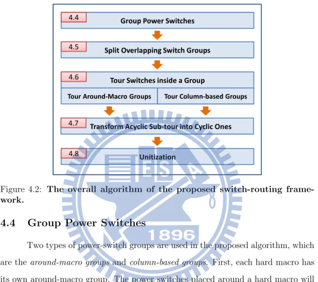
Figure 4.2 illustrates the overall flow of the proposed switch-routing frame-work, which contains five major steps: (1) group power switches, (2) split the overlapping groups into non-overlapping ones, (3) tour the power switches inside a non-overlapping group, (4) transform acyclic sub-tours into cyclic ones, and (5) merge all cyclic sub-tours into one. The details of each step will be introduced in the following subsections.
15
Group Power Switches 4.4
Split Overlapping Switch Groups 4.5
Transform Acyclic Sub-tour into Cyclic Ones 4.7
Unitization 4.8
Tour Switches inside a Group 4.6
Tour Around-Macro Groups Tour Column-based Groups
Figure 4.2: The overall algorithm of the proposed switch-routing frame-work.
4.4
Group Power Switches
Two types of power-switch groups are used in the proposed algorithm, which are the around-macro groups and column-based groups. First, each hard macro has its own around-macro group. The power switches placed around a hard macro will be assigned to its around-macro group. Note that one power switch may be assigned to two around-macro groups simultaneously since it may locate just in between two nearby hard macros. Next, the rest power switches are divided into different column-based group column-based on its column index in the position matrix. The power switches in a column-based group will not overlap with the power switches in any other group. Note that the reason why we group the rest switches based on column index instead of row index is that the distance between two vertically adjacent switches is much shorter than the distance between two horizontal adjacent switches based on the result of the adopted switch-allocation tool. So touring the switches in the vertical
16 direction is more preferred than the horizontal direction.
4.5
Split Overlapping Switch Groups
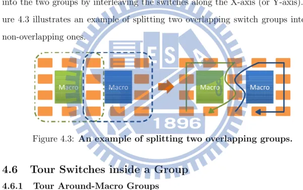
The power switches in two around-macro groups may overlap, such a scenario happens when one row (or column) of switches are embedded just in between two hard macros. The objective of this step is to separate those overlapped switches into the two groups by interleaving the switches along the X-axis (or Y-axis). Fig-ure 4.3 illustrates an example of splitting two overlapping switch groups into two non-overlapping ones.
Macro Macro Macro Macro
Figure 4.3: An example of splitting two overlapping groups.
4.6
Tour Switches inside a Group
4.6.1 Tour Around-Macro Groups
We first try to tour all the switches in an around-macro group clockwise starting from the most left-bottom one. If no two adjacent switches exceeds the Manhattan-distance constraint, we can form a cyclic sub-tour. Otherwise, the first sub-tour ends at one end of the violating edge, and we start the next sub-tour from the other end of the violating edge. Note that these two sub-tours are both acyclic. We repeat the above process until all switches are visited.
17
(b)
(a)
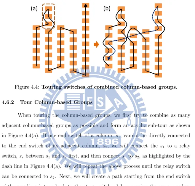
Figure 4.4: Touring switches of combined column-based groups. 4.6.2 Tour Column-based Groups
When touring the column-based groups, we first try to combine as many adjacent column-based groups as possible and form an acyclic sub-tour as shown in Figure 4.4(a). If one end switch of a column, s1, cannot be directly connected
to the end switch of its adjacent column, s2, we will connect the s1 to a relay
switch, sr between s1 and s2 first, and then connect sr to s2, as highlighted by the
dash line in Figure 4.4(a). We will repeat the above process until the relay switch can be connected to s2. Next, we will create a path starting from the end switch
of the acyclic sub-tour back to the start switch while removing the corresponding connection of the original acyclic tour. An example of creating such a cyclic sub-tour is illustrated in Figure 4.4(b). Last, for each remaining dangling column-based groups, we tour the switches from bottom to top to forms an acyclic sub-tour.
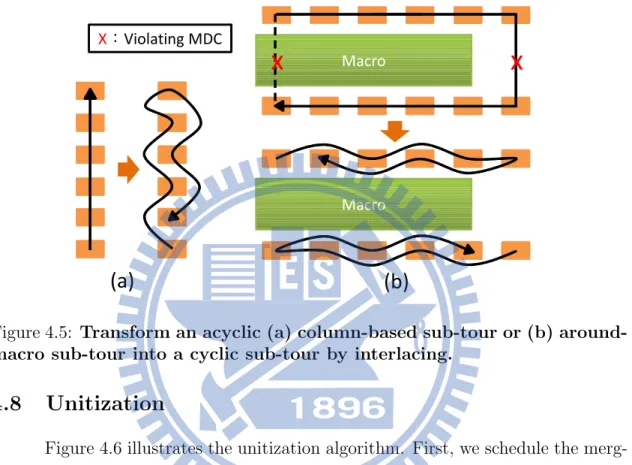
4.7
Transform Acyclic Sub-tour into Cyclic Ones
For each acyclic sub-tour, we interlace the order of its switches to form a cyclic one. Figure 4.5(a) and (b) illustrate the examples of how to interlace the
18 switch order to transform an acyclic column-based tour and around-macro sub-tour into a cyclic one, respectively.
X:Violating MDC
(a)
Macrox
x
Macro(b)
Figure 4.5: Transform an acyclic (a) column-based sub-tour or (b) around-macro sub-tour into a cyclic sub-tour by interlacing.
4.8
Unitization
Figure 4.6 illustrates the unitization algorithm. First, we schedule the merg-ing list for around-macro sub-tours and column-based sub-tours, respectively, based on the locations of sub-tours’ starting point (from lower left to upper right by de-fault). Then we append the merging list of the column-based macros to the end of the merging list of the around-macro sub-tours. Next, we iteratively use the first available sub-tour in the merging list as the current discard sub-tour. Then we at-tempt to identify a pair of adjacent switches, called the connecting switches, inside the discard sub-tour which can satisfy the following two conditions: (1) there exist a pair of connecting switches in another nearby sub-tour, denoted as the augmented sub-tour, where either connecting switch in the discard sub-tour can correspond to a connecting switch in the augmented sub-tour within the search range, and (2) the Manhattan distance between the corresponding connecting switches in the two
19
Algorithm: Unitization 1 begin
2 Schedule merging list for sub-tours around macros. 3 Schedule merging list for sub-tours away from macros. 4 Concatenate the above merging list.
5 Set searching range to Manhattan-distance constraint. 6 while ( exists more than one sub-tour ) {
7 foreach first available discard sub-tour in merging list { 8 Search the best pair of joint switches in discard sub-tour
and obtain the corresponding joint switches in the augmented sub-tour.
10 Merge discard sub-tour into augmented sub-tour. 11 Remove discard sub-tour from merging list. 12 }
13 Increase searching range. 14 }
14 end
Figure 4.6: The algorithm of unitization.
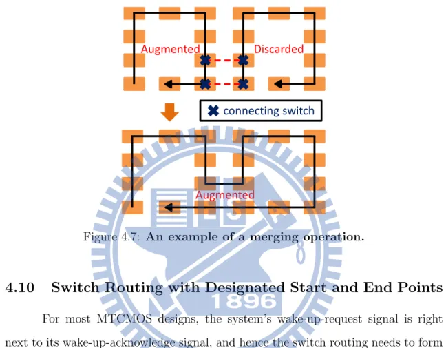
sub-tours is minimum. Once a pair of feasible connecting switches can be found in the discard sub-tour, we can merge it into the corresponding augmented sub-tour by reconnecting the connecting switches as shown in Figure 4.7. Finally, we remove the discard sub-tour from the merging list and repeat the above process for the next available sub-tour in the merging list until all the sub-tours are tried.
If more than one sub-tours are left in the merging list after this iteration, we increase the searching range and repeat the above iteration until only one sub-tour is left. The remaining sub-tour is the final Hamiltonian-cycle routing for the power switches.
4.9
Merging Operation
Figure 4.7 illustrates how a merging operation in the proposed algorithm can merge the discard sub-tour into the augmented sub-tour. Note that the modified
20 augmented sub-tour is still cyclic after the merging operation.
Augmented
connecting switch
Augmented Discarded
Figure 4.7: An example of a merging operation.
4.10
Switch Routing with Designated Start and End Points
For most MTCMOS designs, the system’s wake-up-request signal is right next to its wake-up-acknowledge signal, and hence the switch routing needs to form a Hamiltonian cycle. However, for some seldom cases, the wake-up-request signal is far apart from the wake-up-acknowledge signal, so that the switch routing here needs to find a Hamiltonian-path tour starting from the location of the wake-up-request and ending at the location of the wake-up-acknowledge signal. Our proposed frame-work also provide an operation, called stretching, to turn a feasible Hamiltonian-cycle routing into a feasible Hamiltonian-path routing with designated start and end points.
The stretching operation will first cut the original Hamiltonian cycle at the designated start point and end point, which breaks the original Hamiltonian cycle into two acyclic sub-tours. Then we apply the splitting operation (as shown in
21 Section 4.5) to turn one acyclic sub-tour into a cyclic one and reconnect it with the other acyclic sub-tour. Figure 4.8 illustrates an example of applying the stretching operation.
new starting switch
old starting switch
new ending switch
old ending switch
Chapter 5
Experimental Results
The experiments in this section are conducted based on three power-gated domains in a 4G-application MTCMOS design, which is implemented with a TSMC 40nm low-power cell library. The Manhattan-distance constraint is set to 80µm. Table 5.1 first shows the experimental result after applying the proposed switch-routing framework. In Table 5.1, Column 2 lists the total number of power switches used in a domain. Column 3 and 4 list the maximum Manhattan distance and the total Manhattan distance. Column 5 and 6 list the wire length of the resulting switch routing and the total wire length of the domain reported by Encounter. Column 7 lists the total runtime consumed by the proposed framework in seconds.
Table 5.1: Routing results of the proposed switch-routing framework on 3 power-gating domains.
power # of max MD total MD routing wire length (µm) runtime domain switch (µm) (µm) switch total (sec) Case 1 31559 78.12 411137.42 456065 80510465 3.81 Case 2 18813 75.60 254320.61 283742 47743977 2.59 Case 3 27190 78.12 335451.14 371419 46339737 4.42
The result in Table 5.1 first shows that the proposed switch-routing frame-work can always generate a feasible Hamiltonian-cycle routing without violating the Manhattan-distance constraint for all three cases, which demonstrates the
23 fectiveness of the proposed framework. Also, the longest runtime of the proposed framework is less than 5 seconds for the three cases, which demonstrates the effi-ciency of the proposed framework and its scalability to large industrial MTCMOS designs. Note that the wire length of the switch routing is at most 0.8% of the total wire length in a domain, showing that minimizing the wire length of switch routing is indeed a secondary issue when designing a power-gated domain.
Table 5.2 further shows some simulation result regarding the switch routing generated in Table 5.1. In Table 5.2, Column 2 lists the response time from the wake-up-request signal to the wake-up-acknowledge signal reported by Encounter. Column 3 lists the power-up time, defined as the time that the virtual VDD rise from ground to 99.5% of the true VDD (1.1V). Column 4 lists the peak current consumed during the sleep-to-active mode transition. The results of Column 3 and 4 are reported by a power-analysis tool [28].
Table 5.2: Simulation results of the proposed switch-routing framework on 3 power-gating domains.
power response time power-up time peak current domain (ns) (ns) (mA) Case 1 23096.25 1279.92 76.99 Case 2 13764.30 991.32 59.59 Case 3 21206.20 1181.55 66.64
Next, we attempt to solve the switch-routing problem by applying a TSP solver based on a modified complete graph as described in Section 3.2. Since we set an excessively large weight to each edge whose distance between its two switches ex-ceeds the constraint, the TSP solver should avoid passing through such a constraint-violated edge while minimizing the total path length. If the TSP solver is optimal enough, no constraint-violated edge will be visited and hence a feasible Hamiltonian-cycle can be found.
24 We try to apply a state-of-the-art TSP solver [22] to solve the switch-routing problem and check whether this advanced TSP solver can generate a feasible Hamiltonian-cycle without going through any constraint-violated edge. The TSP solver [22] can be obtained from public domain and has been applied to solve several optimization problems [25] [26] [27]. Also, this TSP solver [22] can always iteratively fine-tune an existing solution to obtain a better solution. However, this TSP solver [22] requires a two-dimensional matrix to store all edges’ weight of the complete graph.
Table 5.3 compares the maximum and total Manhattan-distance of the re-sulting Hamiltonian-cycle, the number of constraint-violated edges, and the runtime between the proposed framework and the TSP solver [22]. For Case 1 and Case 3, the TSP solver [22] cannot generate any result since building the corresponding data structure to store all edge’s weight will run out of memory at a workstation with 32GB main memory and 16 AMD64 cores. For Case 2, the resulting Hamiltonian cycle reported by the TSP solver [22] still contains few edges violating the constraint after running 100 iterations. Its runtime is 7243 seconds, which is 2796 times of the runtime consumed by the proposed framework. Even though we keep on running more iterations for over one day, the three constraint-violated edges still cannot be removed. This result demonstrates that a feasible Hamiltonian-cycle routing, which can be efficiently and effectively obtained by applying the proposed switch-routing framework, cannot be easily obtained by applying a general TSP solver.
25
Table 5.3: Comparison between the proposed framework and a TSP solver [22].
power max MD total MD # of MD runtime domain method (µm) (µm) violations (sec) Case 1 Proposed 78.12 411137.42 0 3.81
TSP [22] N.A. N.A. N.A. N.A. Case 2 Proposed 75.60 254320.61 0 2.59
TSP [22] 2363.07 148378.00 3 7243 Case 3 Proposed 78.12 335451.14 0 4.42 TSP [22] N.A. N.A. N.A. N.A.
Chapter 6
Conclusion
In this thesis, an efficient framework has been proposed to generate a Hamiltonian-cycle switch routing that can satisfy the Manhattan distance constraint and avoid the connection traveling across the hard macros. This Hamiltonian-cycle switch routing can support both the single-input and double-input power switches provided by current TSMC coarse-gain MTCMOS libraries, which cannot be both supported by applying the previous switch-routing framework [21]. The proposed framework can also handle the switch routing with arbitrary locations of its wake-up-request signal and wake-up-request signal. The experimental result demonstrates the ef-ficiency and effectiveness of the proposed framework by comparing it with a TSP solver based on industrial MTCMOS designs. The proposed switch-routing frame-work is compliant to the environment of a commercial APR tool [10] and has helped taping out multiple MTCMOS designs inside a major design-service company.
Bibliography
[1] S. Mutoh, T. Douseki, Y. Matsuya, T. Aoki, and J. Yamada, 1V high-speed digital circuit technology with 0.5gm multi-threshold CMOS, in Proc. IEEE 6th Interna-tional Annual ASIC Conference, pp.186-189, 1993.
[2] K. Roy, S. Mukhopadhyay, and H. Mahmoodi-Meimand, ”Leakage Current Mecha-nisms and Leakage Reduction Techniques in Deep-Submicrometer CMOS Circuits,” Proceeding of the IEEE, vol. 91, No. 2, Feb. 2003, pp. 305-327.
[3] J. Kao, S. Narendra, and A. Chandrakasan, Subthreshold Leakage Modeling and Reduction Techniques, ACM/IEEE International Conference on Computer Aided Design, pp.141-148, Nov., 2002.
[4] C. Long and L. He, Distributed Sleep Transistors Network for Power Reduction, ACM/IEEE Design Automation Conference, pp.181-186, July 2003.
[5] M. Anis, S. Areibi, and M Elmasry, Design and Optimization of Multithreshold CMOS (MTCMOS) Circuits, IEEE Trans. on Computer-Aided Design of Integrated Circuits and Systems, pp.1324-1342, Volume 22, Issue 10, Oct. 2003.
[6] A. Ramalingam, A. Devgan, and D. Z. Pan, Wakeup Scheduling in MTCMOS Circuits Using Successive Relaxation to Minimize Ground Bounce, JOURNAL OF LOW POWER ELECTRONICS, pp.1-8, Vol.3, No.1, 2007.
[7] H. Jiang and M. Marek-Sadowska, Power Gating Scheduling for Power/Ground Noise Reduction, ACM/IEEE Design Automation Conference, pp.980-985, June 2008.
[8] A. Abdollahi, F. Fallah, and M. Pedram, A Robust Power Gating Structure and Power Mode Transition Strategy for MTCMOS Design, IEEE Trans. on Very Large Scale Integration Systems, pp.80-89, Volume 15, Issue 1, Jan. 2007.
[9] Taiwan Semiconductor Manufacturing Company, Ltd., TSMC Reference Flow 7.0, 2007.
[10] Cadence, ”Encounder User Guide,” version v09.12-s159 1.R
[11] C. Long and L. He, Distributed sleep transistor network for power reduction, IEEE Transactions on Very Large Scale Integration (VLSI) Systems, Vol. 12, Issue 9, pp. 937–946, 2004.
28
[12] S. Mutoh, S. Shigematsu, Y. Matsuya, H. Fukuda, T. Kaneko, and J. Yamada, A 1-v multithreshold-1-voltage CMOS digital signal process for mobile phone application, IEEE J. Solid-State Circuits, Vol. 31, pp. 1795–1802, 1996.
[13] J. Kao, S. Narendra, and A. Chandrakasan, MTCMOS hierarchical sizing based on mutual exclusive discharge patterns, Proceeding of Design Automation Conference, pp. 495–500, 1998.
[14] K. Shi and D. Howard, Sleep transistor design and implementation-Simple concepts yet challenges to be optimum, Proceeding of VLSI-DAT, pp. 1–4, 2006.
[15] M. Anis, S. Areibi, M. Mahmoud, and M. Elmasry, Dynamic and leakage power re-duction in MTCMOS circuits using an automated efficient gate clustering technique, Proceeding of Design Automation Conference, pp. 480–485, 2002.
[16] Y. Lee and T. Kim, Technique for controlling power-mode transition noise in dis-tributed sleep transistor network, Asia and South Pacific Design Automation Con-ference (ASP-DAC), pp. 131–136, 2010.
[17] H. Jiang; M. Marek-Sadowska, Power/Ground Supply Network Optimization for Power-Gating, International Conference on Computer Design, pp. 332–337, 2006. [18] H. Jiang; M. Marek-Sadowska, Power gating scheduling for power/ground noise
reduction, Proceeding of Design Automation Conference, pp. 980–985, 2008. [19] S. Kim, S. V. Kosonocky, and D. R. Knebel, Understanding and minimizing ground
bounce during mode transition of power gating structures, International Symposium on Low Power Electronics and Design, pp. 22–25, 2003.
[20] R. Bhanuprakash, M. Pattanaik, S. S. Rajput, and K. Mazumdar, Analysis and reduction of ground bounce noise and leakage current during mode transition of stacking power gating logic circuits, IEEE Region 10 Conference TENCON, pp. 1–6, 2009.
[21] T. M. Tseng, Mango C. T. Chao, C. P. Lu, and C. H. Lo, Power-Switch Routing for Coarse-Grain MTCMOS Technologies, ACM/IEEE International Conference on Computer Aided Design (ICCAD), 2009.
[22] D. Applegate, R. Bixby, V. Chvatal, and W. Cook, Concorde TSP Solver, http://www.tsp.gatech.edu/concorde/index.html.
[23] C. Fremuth-Paeger, B. Schmidt, and B. Eisermann, GOBLIN:A Graph Object Library for Network Programming Problems, http://www.math.uni-augsburg.de/ fremuth/goblin.html.
[24] K. Helsgaun, LKH: An Effective Implementation of the Lin-Kernighan Heuristic for solving TSP, http://akira.ruc.dk/ keld/research/LKH/.
29
[25] D. Aldous and A. G. Percus, Scaling and Universality in Continuous Length Com-binatorial Optimization, PROC. Nat. Acad. Sci. USA 100 (20), pp.11211-11215, 2003.
[26] D. Applegate, W. Cook, S. Dash, and A. Rohe, Solution of a Min-Max Vehicle Routing Problem, INFORMS Journal on Computing 14 (2), pp.132-143, 2002. [27] G. Gutin, H. Jakubowicz, S. Ronen, and A. Zverovitch, Seismic Vessel Problem,
Communications in DQM 8, pp.13-20, 2005.