國立交通大學
電機學院光電工程研究所
碩 士 論 文
解決小尺寸色序法液晶顯示器
之色分離現象
Demonstration of a Mobile-Sized Field Sequential
Color LCD for Color Break-up Suppression
研究生:吳建良
指導教授:謝漢萍教授
黃乙白助理教授
解決小尺寸色序法液晶顯示器
之色分離現象
Demonstration of a Mobile-Sized Field Sequential
Color LCD for Color Break-up Suppression
研究生:吳建良 Student: Chien-Liang Wu
指導教授:謝漢萍 Advisor: Han-Ping D. Shieh
黃乙白 Yi-Pai Huang
國立交通大學
電機學院光電工程研究所
碩士論文
A Thesis
Submitted to Institute of Electro-optical Engineering
College of Electrical Engineering
National Chiao Tung University
in Partial Fulfillment of the Requirements
for the Degree of Master
in
Electro-Optical Engineering
Hsinchu, Taiwan, Republic of China
i
解決小尺寸色序法液晶顯示器之色分離現象
碩士研究生: 吳建良
指導教授: 謝漢萍 教授
黃乙白 助理教授
國立交通大學
光電工程研究所碩士班
Abstract (Chinese)
色序法顯示器原理是利用三原色場循序顯示的時間混色法來混出所有顏色,取代 了傳統液晶顯示器的空間混色法。這種顯示法具備了以下的優點:高色彩飽和度、高光 穿透度、高解析度以及低功率消耗,但此種顯示器卻衍生出一個問題,我們稱之為色分 離現象,這個現象將會影響到人眼觀看影像的品質,是一個不可忽視的問題。 基於以上的論述,我們提出了兩個可以有效解決靜態以及動態色分離現象的方法。 第一個方法為:RGBWmin,此方法可以有效的抑制靜態的色分離現象;第二個方法為; Five Color Field Arrangement with Wmin (5-CFA with Wmin),此方法不僅可以抑制靜態色分 離現象,也可以有效的解決動態色分離現象。最後我們將這些方法實現於 5.6 吋的色序 法液晶顯示器上,並使用此硬體架構做進一步的實驗,也成功驗證了我們所提出解決色 分離方法的可行性。ii
Demonstration of a Mobile-Sized Field Sequential
Color LCD for Color Break-up Suppression
Student: Chien-Liang Wu Advisors: Prof. Han-Ping D. Shieh
Prof. Yi-Pai Huang
Institute of Electro-Optical Engineering
National Chiao Tung University
Abstract
The Field Sequential Color (FSC) LCD displays red, green and blue fields sequentially to mix a full color image by temporal color mixing method. It has some advantages, such as high transmittance, high resolution, high color saturation and low power consumption. However, color break-up (CBU) is a serious issue to reduce image quality.
We proposed two methods for reducing CBU phenomenon. First one is RGBWmin, which can reduce static CBU by reducing the intensities of R, G, and B fields. The other one is Five Color Field Arrangement with Wmin (5-CFA with Wmin), which combines RGBWmin and color field arrangement to suppress dynamic and static CBU simultaneously. These two methods were successfully implemented in a 5.6-inch Optically Compensated Bend (OCB) mode FSC-LCD. Finally, we used the 5.6-inch FSC-LCD and a high speed camera to experiment for static and dynamic CBU. The experimental results reveal that static CBU were reduced by inserting a Wmin field. Furthermore, dynamic CBU were eliminated by using 5-CFA with Wmin method.
~ iii ~
Acknowledgement
首先,由衷感謝指導教授謝漢萍老師及黃乙白老師提供良好的研究設備與學習環 境,讓我們在專業能力、語言能力以及研究領域上能有很好的成果,也感謝老師能在我 遇到問題時,給予方向與指教,讓我對我的研究題目更了解,進而完成了” 解決小尺 寸色序法液晶顯示器之色分離現象”之論文。 在實驗室的日子裡,首先要感謝已畢業的雅婷學姊,以及博班均合學長和芳正學 長在實驗與專業知識上的指導與協助,使我在研究所這段日子學到許多。而實驗室的其 他博班學長姐們鄭榮安博士、企桓學長、裕國學長、喬舜學長、仁宇學長、柏儒學長, 提供了許多寶貴的經驗與意見,讓我受益良多。同時我要感謝我的同學們:其霖、勝昌、 宛徵、明農、景明、凌嶢、國振、仁杰在研究、生活上的幫助與分享,並陪伴我一起度 過這兩年的碩士生涯。同時也感謝實驗室的學弟妹與助理小姐們的幫忙及讓實驗是充滿 歡愉的氣氛。 最後,對於我的家人與女朋友,我要感謝你們多年來的支持與鼓勵以及生活上的 細心照顧,使我能故無後顧之憂的研究與學習,並順利完成碩士學位。這份喜悅與榮耀 我將跟所有我所認識的各位分享。~ iv ~
Table of Contents
ABSTRACT (CHINESE) ... I ABSTRACT ... II ACKNOWLEDGEMENT ... III TABLE OF CONTENTS ... IV FIGURE CAPTION ... VII LIST OF TABLES ... XCHAPTER 1 ... 1
INTRODUCTION ... 1
1.1 LIQUID CRYSTAL DISPLAYS (LCDS) ... 1
1.2 FIELD SEQUENTIAL COLOR LIQUID CRYSTAL DISPLAYS (FSC-LCDS) ... 2
1.3 PHENOMENON OF COLOR BREAK-UP (CBU) ... 4
1.4 MOTIVATION AND OBJECTIVE ... 5
1.5 ORGANIZATION ... 6
CHAPTER 2 ... 7
COLOR BREAK-UP MECHANISM AND PRIOR SOLUTIONS ... 7
2.1 PHYSIOLOGY OF EYE MOVEMENT ... 7
2.1.1 Saccade ... 7
2.1.2 Smooth pursuit ... 8
2.2 MECHANISM OF COLOR BREAK-UP IN CONVENTIONAL FSC-LCD ... 9
~ v ~
2.2.2 Static CBU ... 11
2.3 PRIOR METHODS FOR CBU REDUCTION ... 12
2.2.1 Frame frequency increase ... 12
2.2.2 Motion interpolation ... 13
2.2.3 Four color field arrangement (4-CFA) ... 15
2.2.4 Summary ... 16
CHAPTER 3 ... 17
RGBWMIN AND 5-CFA WITH WMIN METHODS ... 17
3.1 RGBWMIN METHOD ... 17
3.2 5 COLOR FIELD ARRANGEMENT WITH WMIN METHOD (5-CFA WITH WMIN) ... 21
3.3 DISCUSSION ... 23
3.4 SUMMARY ... 25
CHAPTER 4 ... 26
IMPLEMENTAL AND EXPERIMENTAL RESULTS ... 26
4.1 HARDWARE:A5.6-INCH FSC-LCD SYSTEM ... 26
4.1.1 5.6-inch FSC-LCD ... 27
4.1.1.1 OCB mode liquid crystal ... 27
4.1.1.2 Source and gate drivers ... 29
4.1.1.3 LED backlight system ... 32
4.1.2 Field Programmable Gate Array (FPGA) ... 34
4.2 IMPLEMENT THE PROGRAMS OF THE LC AND LED CONTROLLERS WITH RGBWMIN AND 5-CFA WITH WMIN METHODS ... 35
~ vi ~
4.2.1.1 Process 1: input pattern convert to input data buffers ... 36
4.2.1.2 Process 2: the data access of frame buffers ... 39
4.2.1.3 Process 3: shift data from frame buffers to data buffers ... 40
4.2.2 Module design of FSC controller for 5-CFA with Wmin method ... 41
4.2.3 Module design of LED controller ... 42
4.2.4 Simulation and implementation of FSC controller and LED controller ... 43
4.2.5 The specifications of the 5.6-inch FSC-LCD ... 46
4.3 EXPERIMENTAL RESULTS IN RGBWMIN AND 5-CFA WITH WMIN METHODS ... 48
4.3.1 Static CBU suppression ... 48
4.3.2 Dynamic CBU suppression ... 49
4.4 SUMMARY ... 53
CHAPTER 5 ... 54
CONCLUSIONS AND FUTURE WORKS ... 54
5.1 CONCLUSIONS ... 54
5.2 FUTURE WORKS ... 55
~ vii ~
Figure Caption
FIG.1.1THE CONFIGURATION OF (A) CONVENTIONAL LCD AND (B)FSC-LCD ... 2
FIG.1.2THE DISPLAY MECHANISM OF A FSC-LCD ... 4
FIG.1.3TIMING DIAGRAM OF A FSC-LCD ... 4
FIG.1.4(A)AN ORIGINAL IMAGE AND (B)CBU IMAGE ... 5
FIG.2.1AN EXAMPLE OF SACCADE EYE MOVEMENT ... 8
FIG.2.2 THE SCHEME OF CBU PHENOMENON IN A CONVENTIONAL FSC-LCD ... 10
FIG.2.3(A)THE RELATIONSHIP BETWEEN TIME AND DISPLAY POSITION OF A ... 10
FIG.2.4(A)IMAGE IN AN FSC-LCD AND PATH OF A SACCADE. ... 12
FIG.2.5 THE RELATIONSHIP BETWEEN TIME AND LOCATION OF A MOVING IMAGE IN ... 13
FIG.2.6SCHEME OF (A) CONVENTIONAL AND (B) MOTION INTERPOLATION METHOD IN AN FSC-LCD. ... 14
FIG.2.7A CROSSING OBJECT IS MOVING FROM LEFT TO RIGHT AT SPEED S AND THE ... 14
FIG.2.8(A) THE COLOR ORDER AND (B) THE RELATIONSHIP BETWEEN TIME ... 15
FIG.3.1THE FLOW CHART OF RGBWMIN ALGORITHM ... 18
FIG.3.2THE CUB SIMULATION IMAGES BY USING (A)RGB AND (B)RGBWMIN METHODS ... 19
FIG.3.3(A)THE CBU SIMULATION IMAGES IN SKY BLUE AND STRONG RED ... 20
FIG.3.4(A)THE COLOR ORDER AND (B) EYES PURSUING A MOVING IMAGE ... 21
FIG.3.5OBSERVER PERCEIVES AN IMAGE IN FOUR CONTINUOUS FRAMES (A)CONVENTIONAL COLOR SEQUENCE (B)5-CFA WITH WMIN COLOR SEQUENCE. ... 23
~ viii ~
... 27
FIG.4.2 THE TRANSITION BETWEEN SPLAY AND BEND STATES IN AN OCB MODE LC ... 28
FIG.4.3 THE TRANSITION CURVE FROM SPLAY TO BEND STATE IN OCB MODE LC ... 29
FIG.4.4 TIMING DIAGRAM WITH A BLANK INSERTION TIME IN THE CONVENTIONAL FSC-LCD ... 29
FIG.4.5THE TIMING DIAGRAM OF RSDS ... 31
FIG.4.6 SERIAL DATA INPUT TIMING DIAGRAM OF THE LED CONTROLLER ... 33
FIG.4.7 THE TOP VIEW OF LED DRIVER AND LED BACKLIGHT ... 34
FIG.4.8 THE RELATIONSHIP BETWEEN EACH MODULE OF FSC CONTROLLER ... 36
FIG.4.9THE 24-BIT W DATA OF THREE PIXELS IS OUTPUT AT 1ST FALLING EDGE OF CLOCK. ... 37
FIG.4.10THE 24-BIT R’ DATA OF THREE PIXELS IS OUTPUT AT 2ND FALLING EDGE OF CLOCK. ... 38
FIG.4.11THE 24-BIT G’ DATA OF THREE PIXELS IS OUTPUT AT 4TH FALLING EDGE OF CLOCK. ... 38
FIG.4.12THE 24-BIT B’ DATA OF THREE PIXELS IS OUTPUT AT 6TH FALLING EDGE OF CLOCK. ... 39
FIG.4.13 THE SDRAM ACCESS BETWEEN INPUT AND OUTPUT DATA BUFFERS ... 41
FIG.4.14THE COLOR SEQUENCE CAN BE CHANGED BY INSERTING A STATE MACHINE. ... 42
FIG.4.15 GRAYSCALE PWM CYCLE TIMING DIAGRAM ... 43
FIG.4.16 THE SIMULATION RESULT OF FSC CONTROLLER WITH RGBWMIN METHOD ... 45
FIG.4.17 THE SIMULATION RESULT OF FSC CONTROLLER WITH 5-CFA WITH WMIN METHOD ... 45
FIG.4.18 THE CONTROL PROCESSES IN THE 5.6-INCH FSCLCD PLATFORM ... 47
FIG.4.19 THE DISPLAYED IMAGE ON THE 5.6-INCH FSCLCD ... 47
FIG.4.20THE IMAGES DISPLAYED BY A 5.6-INCH FSC-LCD WITH ... 48
FIG.4.21 THE STATIC CBU IMAGES FOR (A)RGB AND (B)RGBWMIN METHODS ... 49
FIG.4.22 THE EXPERIMENTAL CONSTRUCT ... 50
FIG.4.23THE EXPERIMENTAL RESULTS WITH AND WITHOUT RGBWMIN ... 50
FIG.4.24 THE HISTOGRAM OF RCS IN THREE COLOR IMAGES ... 51
~ ix ~
FIG.4.26 THE EXPERIMENTAL RESULTS FOR 5-CFA WITH WMIN METHOD ... 53
FIG.5.1 THE R,G,B, AND WMIN FIELDS OF AN IMAGE ... 55
~ x ~
List of Tables
TABLE 3.1THE RELATIONSHIPS BETWEEN T AND RESOLUTIONS ... 24
TABLE 4.1 THE SPECIFICATIONS OF (A) THE GATE DRIVER AND ... 31
TABLE 4.2 THE SPECIFICATIONS OF LED DRIVER ... 33
TABLE 4.3 THE FIELD TIME BASED ON RGBWMIN AND 5-CFA WITH WMIN METHODS IN A 5.6-INCH
~ 1 ~
Chapter 1
Introduction
___________________________________________________________________________
1.1 Liquid Crystal Displays (LCDs)
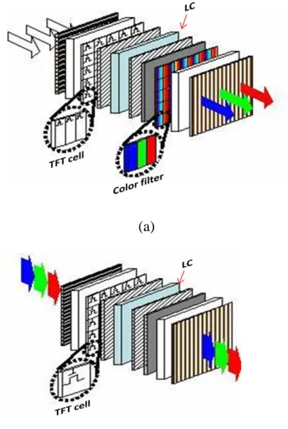
A liquid crystal display (LCD) has become more and more popular, because it is much thinner and lighter than a Cathode Ray Tube (CRT) display. The power consumption of LCD is also lower than that of CRT display. An LCD consists of backlight, Thin Film Transistor (TFT) array, Liquid Crystal (LC) layer and color filter, as shown in Fig. 1.1(a). An LCD is a display device made up of any number of color pixel in front of a light source. Each pixel is divided into three sub-pixels, which are colored red, green, and blue, respectively by an additional filter. By controlling the voltage applied across the liquid crystal layer in each pixel, light can be allowed to pass through in varying amounts thus constituting different gray levels. Light pass through the color filter in varying amounts thus a LCD can display a full color image.
A pixel of color filter is divided into three sub-pixels, red (R), green (G) and blue (B) to mix a full color image by spatial color mixing method. Thus, the resolution and light transmittance will be reduced in conventional LCDs. Therefore, how to enhance the light efficiency is a main issue of LCD.
~ 2 ~
(a)
(b)
Fig. 1.1 The configuration of (a) conventional LCD and (b) FSC-LCD
1.2 Field sequential color liquid crystal displays (FSC-LCDs)
The main components of FSC-LCD are LED backlight and high response LC. Backlighting for LCD displays, the availability of LEDs in specific colors (R, G, and B) enables a full-spectrum light source which expands the color gamut by as much as 45%. In addition, LEDs produce more lumens per watt than other alternatives. For an FSC-LCD, the Cold Cathode Fluorescent Lamp (CCFL, which is a light source classified as an electronic
~ 3 ~
component) has substituted for high efficient light emitting diode (LED) as the light source of backlight. The backlight is made up of three-primary-color (R, G, and B) LEDs, so a color image can be displayed without color filter by temporal color mixing method. Due to the color-filterless feature and LED backlight, the FSC-LCD is expected as a future display with low power consumption, high transmittance, high color saturation, high resolution, and low material cost [1][2][3].
By using temporal mixing method, the backlight turns on R, G, and B sequentially. The temporal mixing method divides a frame into three fields, as shown in Fig. 1.2. Each field consists of TFT scanning time (tTFT) and LED flashing time (tLED), as shown in Fig. 1.3. In addition, an extra time (tLC) is necessary to wait for LC response. The relationship of tone field time and frame frequency (f) is shown in equation 1-1.
1 3f = tTFT + tLC + tLED (1-1)
According to this equation, the operation time of FSC-LCD is one third of conventional one. If 60Hz is a suitable frequency of an LCD, there is only 5.56ms for TFT scanning time, LC response time and LED flashing time in one field. So a fast response time LC is necessary for reducing tLC, such as optically compensated bend (OCB) mode LC.
~ 4 ~
Fig. 1.2 The display mechanism of a FSC-LCD
Fig. 1.3 Timing diagram of a FSC-LCD
1.3 Phenomenon of color break-up (CBU)
Due to the temporal color mixing method, there is a serious issue on FSC-LCDs, called color break-up (CBU). If there is a relative velocity between a displayed image and human eyes, the CBU will be perceived. The intrinsic visual artifact, color breakup, has shown to degrade
~ 5 ~
visual quality [4][5][6][7][8]. The illustration of CBU phenomenon is shown in Fig. 1.4, we
(a) (b) Fig. 1.4 (a) An original image and (b) CBU image
sense the margin of image like a rainbow. According to the relative motion between human eyes and images, the CBU can be classified into dynamic and static CBU. The detail mechanisms of CBU will be described in section 2.1.
1.4 Motivation and objective
The FSC-LCD has the following advantages. First, by using three primary colors LED backlight, the color saturation can be enhanced. Second, the color filter can be removed, so the light transmittance and resolution is higher than conventional LCD. Third, low power consumption can be achieved. Consequently, The FSC-LCD is potential, especially, for the green products in the future. But the CBU phenomenon will degrade the image quality; this issue needs to be resolved.
For improving the image quality, some methods such as frame frequency increase, motion interpolation, and 4 Color Field Arrangement (4-CFA) were proposed for suppressing CBU phenomenon on FSC-LCDs. However, these methods cannot resolve static and dynamic CBU simultaneously. The objective of our research is to study practical methods for reducing
~ 6 ~
static and dynamic CBU simultaneously, and demonstrate the methods on a 5.6-inch FSC-LCD.
1.5 Organization
This thesis is organized as follows. In Chapter 2, we will describe the eye movement when we perceive a moving or static image. Due to the movement of eyes or image, CBU will be caused on a FSC-LCD. Then, the prior methods for reducing CBU will be mentioned. In
Chapter 3, we will describe the proposed methods for improving the image quality by
reducing CBU phenomenon, called RGBWmin and 5 Color Field Arrangement with Wmin (5-CFA with Wmin). In Chapter 4, we will implement those methods in a 5.6-inch FSC-LCD and then verify our methods for reducing CBU. Finally, conclusions and future works will be given in Chapter 5.
~ 7 ~
Chapter 2
Color break-up Mechanism and Prior Solutions
___________________________________________________________________________
We will describe the mechanism of eye movement: smooth pursuit and saccade. Depending on kinds of eye movement, the CBU phenomenon will be classified into static and dynamic CBU. How to reduce CBU is the key problem. Finally, some prior methods which were been proposed will be described.
2.1 Physiology of eye movement
Eyes are the visual system that has retina, a specialized type of brain tissue consisting of photoreceptors and interneurons. The visual system can convert light into electrochemical signals and then transport the signals along the optic nerve fibers to the brain. Humans use two types of eyes movement to track objects of interest: smooth pursuit and saccade [9].
2.1.1 Saccade
Eye saccade is quick and simultaneous movements of both eyes in the same direction. Saccade is an eye movement that randomly and rapidly moves to scan and perceive an interesting part of an object. One reason for saccade in the human eyes is that the fovea plays a critical role in resolving object, by moving the eyes so that small parts of a scene can be perceived with great resolution. The example of the saccade movement on an image is shown in Fig. 2.1 in which the white line is the movement of the eyes.
~ 8 ~
Fig. 2.1 An example of saccade eye movement
2.1.2 Smooth pursuit
“Smooth Pursuit Eye Movement (SPEM)” is the ability of the eyes to smoothly follow a moving object. Pursuit eye movement can be divided into two stages: open loop pursuit and closed loop pursuit. Open loop pursuit is the visual system's first response to a moving object it wishes to track and typically lasts about 100ms. This stage of pursuit is that visual signals have not yet had time to travel through the visual system and correct the pursuit velocity. The second stage of pursuit is called closed-loop pursuit. This stage lasts from 100ms to the end of eyes pursuit. If you are trying to pursue a target, but that target is getting farther and farther away from your fovea, during closed loop pursuit you will increase the speed of pursuit until you stabilize the image.
~ 9 ~
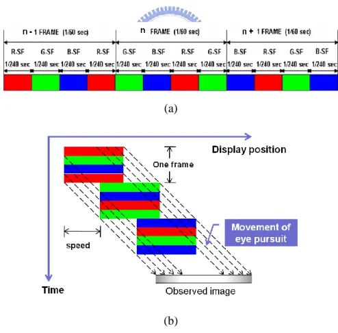
2.2 Mechanism of color break-up in conventional FSC-LCD
By displaying R, G, and B fields sequentially faster than the time resolution of the eye, a good color image can be observed. If there is a relative movement between human eyes and moving object, the field images will be integrated separately on the retina. Therefore, we feel the rainbow effect or CBU on the margin of the image. The mechanism of CBU will show in the following section.
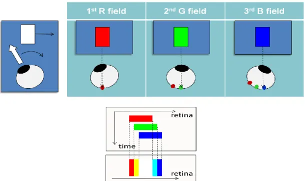
2.2.1 Dynamic CBU
For TV applications, the dynamic CBU phenomenon always occurs at the edge of moving image on a FSC-LCD. The reason for CBU is considered to be caused by temporal integration on the retina of human eyes. The mechanism of dynamic CBU is due to “Smooth Pursuit Eye Movement (SPEM)” in the visual system. Smooth pursuit is movement that smoothly tracks a moving object in visual system. The purpose of smooth pursuit is to perceive a continue moving object. Due to this reason, dynamic CBU can be perceived if three fields alternate slower than the SPEM.
If there is a white image moving from left to right on a FSC-LCD, as shown inFig. 2.2. Human eyes pursue this moving image at the same time. While displaying an image which moves from an initial pixel to the next one, an FSC-LCD will display R, G, and B fields on the initial pixel, then display three fields again on the next pixel. But human eyes will shift while displaying three fields. Thus, R, G, and B fields will separately project on the retina. After integrating in the human visual system, dynamic CBU can be perceived.
~ 10 ~
Fig. 2.2 the scheme of CBU phenomenon in a conventional FSC-LCD
(a)
(b)
Fig. 2.3 (a) The relationship between time and display position of a simulation scheme and (b) CBU image in a visual system
~ 11 ~
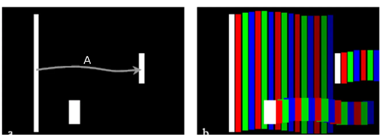
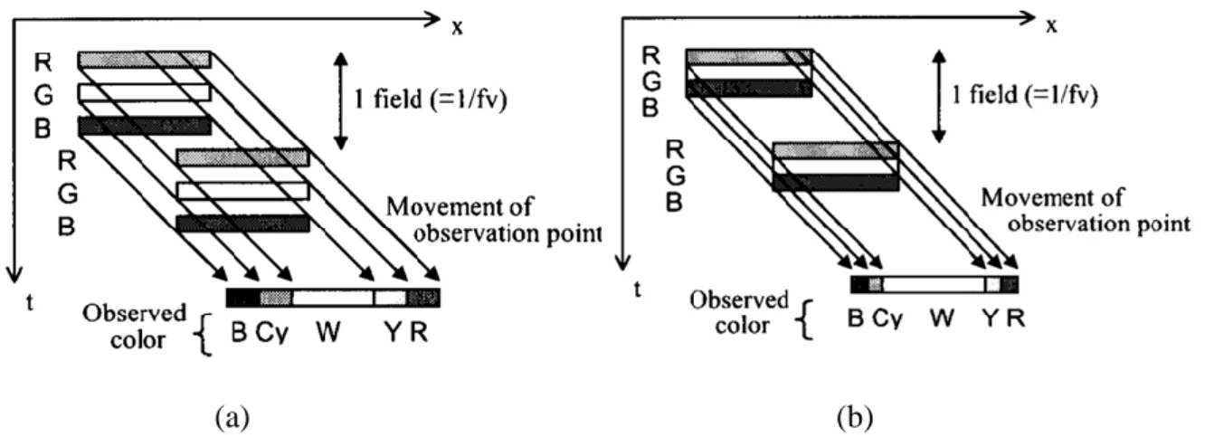
We can simulate the integration of the visual system by using matlab software, as shown in Fig. 2.3(a) which is the relationship between time and display location (horizontal display direction). In this figure, a white bar moves from left to right at 3 pixels per frame. The dotted lines represent the shift of the observer’s viewpoint. When the observer watches a moving image, observer will shift the viewpoint to follow the moving image. Consequently, the observer will recognize an image as shown in Fig. 2.3 (b). This simulation scheme will be used in the following chapters.
2.2.2 Static CBU
For a stationary image, CBU is observed during or after a saccadic eyes movement. Saccade is an eye movement that randomly and rapidly moves to scan and perceive target image. If there are several white images as shown in Fig. 2.4, eye will perceive part of the image that attracts interest. Human’s visual system will be sensitive to white bars in this case, as shown in Fig. 2.4(a), line-A represents the eye saccade movement. Saccade eye movement is much faster than SPEM, the stationary image seems to break up into several field colors, as shown in Fig. 2.4(b).
~ 12 ~
Fig. 2.4 (a) Image in an FSC-LCD and path of a saccade. (b) Observed CBU during or just after the saccade [10].
Static CBU is a serious issue due to the high velocity and random direction of eye saccade movement. We can only increase frame frequency or decrease the luminance of three fields to suppress static CBU in FSC-LCDs.
2.3 Prior methods for CBU reduction
More and more researchers try to find methods for solving CBU phenomenon, such as frame frequency increasing [11][12], motion interpolation [13], and Four Color Field Arrangement (4-CFA) [14]. These proposed methods will be described in detail.
2.2.1 Frame frequency increase
As mentioned before, increasing the frame frequency is a method to suppress the static CBU phenomenon. This is because the R, G, and B fields’ flash time will decrease. As we know, CBU is caused by three fields images separately project on the retina. If the fields’ flash time is shorter, the CBU width is narrower. Some researchers have performed experiments and simulation about threshold frequency that CBU can be eliminated. The threshold
~ 13 ~
frequency in an FSC-LCD is 2 KHz [15][16][17].
(a) (b)
Fig. 2.5 the relationship between time and location of a moving image in (a) single rate and (b) double rate FSC-LCD.
However, the 2 KHz threshold frequency is difficult to achieve because of LC response time is not fast enough. So a double frame rate was demonstrated to suppress dynamic CBU, as shown in Fig. 2.5 which shows the relationship between time and location of a moving image in double frame frequency. The CBU width is just half of original which is driven at a single frame rate.
Due to the fields flash time is reduced by using frame frequency increase method, both dynamic CBU and static CBU can be suppressed. However, the field rate is not fast enough so that this method is limited in CBU reduction.
2.2.2 Motion interpolation
To reduce dynamic CBU, a method called “Adjust of Color Element on the Eyes” (ACE) had been proposed by N. Koma and T. Huchida13, as shown in Fig. 2.6. The R, G, and B fields display on different points which can be calculated according to the speed of the moving object. If human eyes pursue this image, the three fields will be perceived on the same point
~ 14 ~
of the retina, thus dynamic CBU can be totally eliminated.
By using this method, it will be more complicated to calculate the velocity of all the moving images in advance. Moreover, if human does not pursue the moving image, CBU will be more serious, as in Fig. 2.7.
(a) (b)
Fig. 2.6 Scheme of (a) conventional and (b) motion interpolation method in an FSC-LCD.
Fig. 2.7 A crossing object is moving from left to right at speed S and the observer’s eyes trace is moving from right to left at speed M[18].
~ 15 ~
2.2.3 Four color field arrangement (4-CFA)
Four Color Field Arrangement (4-CFA) has proposed by Ya-Ting Hsu14 for suppressing dynamic CBU. The color sequence is ordered as RGBR, GBRG, and BRGB in three continuous frames. The color order is still R, G, and B but the field rate becomes 240Hz, as shown in Fig. 2.8 (a). The relationship between time and display position when eyes pursue a moving image is shown in Fig. 2.8(b). Each eye pursuit movement passes through R, G, and B fields, so the integration of color will be white. Thus, the dynamic CBU can be eliminated. This method is effective in reducing dynamic CBU, so the color field arrangement is suitable for a FSC-LCD. The computation complexity is easier to implement this method in an FSC-LCD. However, this method needs to enhance the ability to suppress static CBU.
(a)
(b)
Fig. 2.8 (a) the color order and (b) the relationship between time and display position in 4-CFA method.
~ 16 ~
2.2.4 Summary
The mechanisms of static and dynamic CBU phenomenon have been presented. In order to improve image quality by reducing CBU, some prior methods have been proposed. However, these methods also have some drawbacks. The LC response time is not fast enough so that the field rate is difficult to achieve 2 KHz. The double frame rate is limited in CBU reduction. By using ACE method, it can be more complicated to calculate image velocity in advance. In addition, this method fails when eyes do not pursue the moving image. Finally, 4-CFA method, the color sequence is ordered as RGBR, GBRG, and BRGB in three continuous frames. 4-CFA method can effectively suppress dynamic CBU, but static CBU is still visible. In the following chapter, we will propose two methods to effectively reduce static and dynamic CBU.
~ 17 ~
Chapter 3
RGBW
minand 5-CFA with W
minmethods
___________________________________________________________________________
The first method for reducing static CBU is called RGBWmin. The second method is to upgrade the first method for suppressing static and dynamic CBU simultaneously, called Five Color Field Arrangement with Wmin (5-CFA with Wmin). Because of the local dimming backlight zones[19] cannot be implemented on mobile-sized FSC-LCDs, we focus on field rate increase for reducing CBU. Therefore, RGBWmin and 5-CFA with Wmin were implemented on a mobile-sized FSC-LCD.
3.1 RGBW
minmethod
In RGBWmin method, one frame was divided into four fields, which were R, G, B, and white (W). The R, G, and B LEDs turn on simultaneously to display a W field. The gray level of each pixel in W field depends on the minimum gray level of corresponding pixel in R, G, and B field. The algorithm of RGBWmin method is shown in Fig. 3.1. The gray levels (GL) of R, G, B, and W field images are represented by GLR, GLG, GLB, and GLW, respectively.
gray level = 255 × T1 γ (3-1)
The relationship between gray level and transmittance are shown in function 3-1, where T is the transmittance of LC and γ is the gamma value of LCD. In RGBWmin algorithm, we assume the gamma value is one. The processes of RGBWmin algorithm are discribed as follows:
~ 18 ~
I. Find out the gray level of each field in one pixel from an image. II. Calculate the minimum gray level from the three fields of this pixel.
III. Subtract the minimum gray level in R, G, and B fields in this pixel, and then assign this new GL to the RGBWmin method.
IV. Assign the minimum gray level to that of the W field in this pixel. V. Repeat the same processes for each pixel of the image.
Fig. 3.1 The flow chart of RGBWmin algorithm
As we mentioned before, CBU is observed because three fields appear separately on the retina. The intensities of R, G, and B fields can be reduced by using the RGBWmin method, so CBU can be suppressed effectively. In addition, image brightness can also be maintained by inserting a W field. In a white image, only the W field will be displayed, thus CBU can be totally eliminated by using RGBWmin method. For other colors, at least one gray level of color fields will be zero.
~ 19 ~
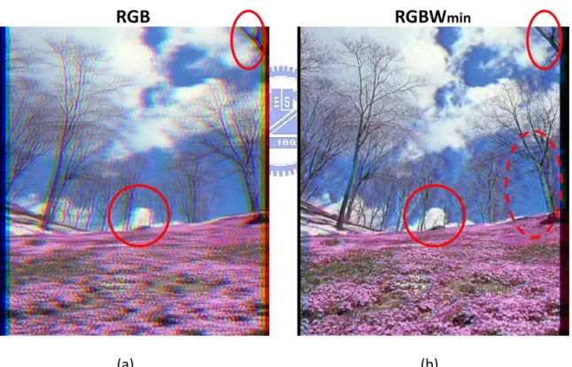
We have simulated an image with conventional RGB and proposed RGBWmin methods, as shown in Fig. 3.2. These images were shifted at 24 pixels per frame to simulate dynamic CBU by using RGBWmin and RGB methods. The image quality can be improved by using RGBWmin, as shown in the area of Fig. 3.2 circled by the solid line. As we mentioned before, the stationary image seems to break up into several color fields due to static CBU. We compare the right and left margins of these two images in Fig. 3.2, the static CBU is suppressed by using RGBWmin method. From the simulation results, RGBWmin method reduces CBU and enhances image quality.
(a) (b)
Fig. 3.2 The CUB simulation images by using (a) RGB and (b) RGBWmin methods
RGBWmin method has artifacts when a specific color image is displayed, as shown in the area of the Fig. 3.2 (b) circled by dotted line. The worst case is the gray level of the first and forth fields do not equal zero, such as sky blue and strong red colors, as shown in Fig. 3.3
~ 20 ~
(a). Dynamic CBU was simulated in a strong red image, as shown in Fig. 3.3(b).The CBU color difference can be suppressed because the gray level of the second field equal to zero and that of the third field is almost equal zero. Thus there are two fields can be seen. If the first and forth fields are seen and integrated by human visual system, CBU width of RGBWmin will be as wide as that of RGB. So in the next section, another method to resolve this issue will be explored.
(a)
(b)
Fig. 3.3 (a) The CBU simulation images in sky blue and strong red (b) The eye pursuit scheme in a strong red image
~ 21 ~
3.2 5 color field arrangement with W
minmethod (5-CFA with W
min)
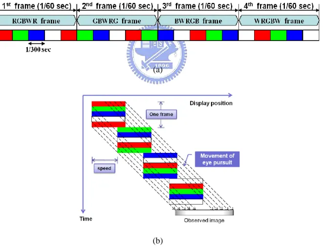
In order to eliminate dynamic CBU, a method is to vary the order of fields in each frame, based on the Ya-Ting Hsu’s research 14. We proposed the method, called 5 Color Field Arrangement with Wmin (5-CFA with Wmin). In this method, the color sequence is arranged as RGBWR, GBWRG, BWRGB, and WRGBW in four continuous frames, as shown in Fig. 3.4 (a). The color sequence is still the same as RGBWmin method but the field rate becomes 300Hz. The algorithm for designing the W field is the same as RGBWmin method. So the advantages of RGBWmin method can be kept in 5-CFA with Wmin method.
(a)
(b)
Fig. 3.4 (a) The color order and (b) eyes pursuing a moving image by using 5-CFA with Wmin method
~ 22 ~
The relationship of time and display location is shown in Fig. 3.4 (b), which describes that eyes pursue a moving image in four continuous frames. The image is integrated by visual system in continuous frames. Each dotted line represents eye movement with a moving image which passes through R, G, B, and W fields in four continuous frames, therefore the visual system will not integrate CBU on the edge of an image.
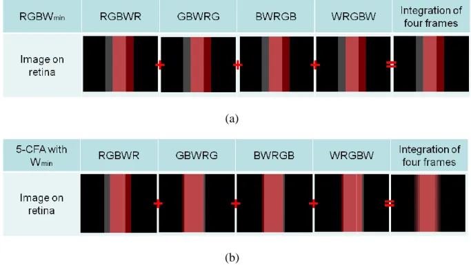
The strong red image simulation result on retina with 5-CFA with Wmin method is shown in Fig. 3.5. If the four continuous frames are perceived and integrated by human visual system, the image on the retina will be compensated at different gray levels in four continuous frames. Consequently, if the dominated field is red, dynamic CBU is the most serious by using RGBWmin method. This is because that human eyes integrate the 1st and the 4th fields.
~ 23 ~
(a)
(b)
Fig. 3.5 Observer perceives an image in four continuous frames (a) Conventional color sequence (b) 5-CFA with Wmin color sequence.
3.3 Discussion
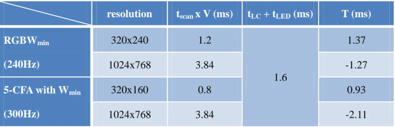
The methods we proposed are suitable for a mobile-sized FSC-LCD, because the field frequency is about 240Hz ~ 300Hz so that the field time is less than 4.17 ms. For a mobile-sized display, the resolution is less so gate driver scanning time is shorter. The relationship between time specifications of an LCD are shown in equation (3-2),
T =1f − tscan × V − tLC − tLED (3-2)
Where f: field rate
tscan: gate driver scanning time of each line V: vertical resolution
~ 24 ~
tLED: LED flash time
According to above equation, if T is larger than zero, the FSC-LCD can be driven at this field rate. For example, we assume the scanning frequency of gate driver is 200 KHz and the scanning time of each line equals 5μs (1 /200 KHz). If a display resolution is 320x160, the gate driver scanning time of a field is 0.8ms (tscan × V =160x 5μs). For a 300Hz field rate, each field time is only 3.33ms. Thus, the time left for LC response and LED flashing is only 2.53ms (3.33-0.8). If the LC response time and LED flash time is 1.6 ms, T will larger than one. If the resolution of a large-sized display is 1024x 768, the gate driver scanning time of each field equals 3.84ms (tscan × V =768x 5μs). Thus, no matter how fast the LC response and LED flash time is, T will always be less than one. Therefore, this FSC-LCD cannot be driven at a 300Hz field rate.
We also calculated the time parameters by using RGBWmin method, as shown in Table 3.1. If the resolution of display is 320x240, T will be 1.37ms. If the resolution is 1024x768, T will be -1.27ms. As these calculation results, the RGBWmin and 5-CFA with Wmin are suitable for mobile-sized FSC-LCDs.
Table 3.1 The relationships between T and resolutions in RGBWmin and 5-CFA with Wmin methods
resolution tscan x V (ms) tLC + tLED (ms) T (ms)
RGBWmin (240Hz) 320x240 1.2 1.6 1.37 1024x768 3.84 -1.27
5-CFA with Wmin
(300Hz)
320x160 0.8 0.93
~ 25 ~
3.4 Summary
The RGBWmin and 5-CFA with Wmin are proposed to suppress CBU. The R, G, and B color fields were lightened so that static CBU were suppressed by using RGBWmin method. However, dynamic CBU still appeared while eyes pursue a moving image for some colors, such as sky blue and strong red. In order to resolve dynamic and static CBU, we proposed 5-CFA with Wmin, combining RGBWmin with color field arrangement method. These novel proposed methods were implemented and verified on a 5.6-inch OCB mode FSC-LCD.
~ 26 ~
Chapter 4
Implemental and Experimental results
___________________________________________________________________________ In the previous chapter, RGBWmin and 5-CFA with Wmin methods were presented for CBU reduction. The objective of this study is to verify that RGBWmin and 5-CFA with Wmin methods can be successfully demonstrated on a 5.6-inch FSC LCD. First of all, the specifications of a 5.6-inch FSC LCD system will be described. Then, the Hardware Description (HDL) language will be explained for demonstrating a 5.6-inch FSC-LCD. Finally, experimental results will be given.
4.1 Hardware: A 5.6-inch FSC-LCD system
A 5.6-inch FSC-LCD system was used in this thesis; this system consists of a Field Programmable Gate Array (FPGA) board, LED controller, LC controller, and a 5.6-inch FSC-LCD. The diagram and specification are shown in Fig. 4.1(a) and (b). The FPGA board is a platform which we used to upload the program and then this board drives the LC and LED controllers. In the following sections, the specifications of FPGA and 5.6-inch FSC-LCD will be described.
~ 27 ~
(a)
(b)
Fig. 4.1 (a) the photograph and (b) the specifications of the 5.6- inch FSC-LCD system
4.1.1 5.6-inch FSC-LCD
4.1.1.1 OCB mode liquid crystal
The OCB mode LC was used in this FSC-LCD to achieve high speed response. In OCB mode LC, the pre-tilt angles in the top and bottom substrates are in opposite directions, as shown in Fig. 4.2, opposite pre-tilt angles result in two important properties. First, it gives rise to the optical self-phase compensation effect on LC directors. As a result, the viewing angle is wide and symmetric. Second, the bend directors in an on-state voltage eliminate the back-flow effect, resulting in a faster response time. As the applied voltage increases, the LC directors
~ 28 ~
change from splay to bend deformation, as illustrated in Fig. 4.3. Below the critical voltage (Vc≈1.8V), splay state is more stable than bend state; above Vc, bend state is more stable [20]. For application, the OCB mode LC will be maintained in bend state by applying a bias voltage. The LC can stay in bend state for a short duration if sufficient high voltage is periodically applied[21][22]. Therefore, we inserted a black frame at the end of each field by applying high voltage to make the LC maintain bend state, as shown in Fig. 4.4. In this way, the OCB mode LCs always remains in bend state to achieve high response ability.
~ 29 ~
Fig. 4.3 the transition curve from splay to bend state in OCB mode LC
Fig. 4.4 timing diagram with a blank insertion time in the conventional FSC-LCD
4.1.1.2 Source and gate drivers
A 480-output TFT-LCD source driver IC with RSDS (Reduced Swing Differential Signaling) was used for the 5.6-inch FSC-LCD, using single 12-bit differential bus conveys 24-bit data. The source driver can receive 12-bit differential data from timing controller and
~ 30 ~
can output 480-channel LCD driving voltage, the specifications are shown in Table 4.1 (a). There are some advantages of the RSDS method, as shown below.
I. Reduced bus width – enables smaller and thinner column driver boards II. Low power dissipation – extends system run time
III. Low Electromagnetic Interference (EMI) generation – eliminates EMI suppression components and shielding
IV. High noise rejection – maintains signal image V. High throughput – enables high resolution displays
For RSDS applications, the timing diagram of data transition is shown in Fig. 4.5. We can see the differential signals are received at the rising edge of clock-P and clock-N. The 24 bit data can be received by using a 12 bit differential bus during one clock-P/N cycle. Then the source driver can transform the received data, and control the LC by applying voltage to 480 output channels.
After the source driver output an electric signal in one line of the frame, the gate driver applies voltage to turn the TFT on. Thus, the source driver’s signal can store into each pixel in one line of the frame. In this way, the LC of each pixel can be controlled individually.
In order to turn TFTs on, a start pulse signal is necessary to drive the gate driver output a high voltage. After a start pulse is triggered, output pins of gate driver will sequentially produce high-driving voltage pulses for the LCD panel. This gate driver can produce voltage through 240 channels to the LCD panel, The max clock frequency is 200 KHz, as shown in Table 4.1 (b).
~ 31 ~
Fig. 4.5 The timing diagram of RSDS
Table 4.1 the specifications of (a) the gate driver and (b) the source driver for the TFT LCD panel
(a) Source driver Output 480 output channels
Input RSDS input interface for low EMI Resolution 8-bit resolution / 256 gray scale
(b) Gate driver Output 240 output channels input clock < 200 KHz
~ 32 ~
4.1.1.3 LED backlight system
The LED backlight system consists of four LED drivers and three in one LEDs (R, G, and B). Each LED driver is a 16-channel constant-current sink driver. Each channel has an individually adjustable 4096-step grayscale by Pulse-Width Modulation (PWM) operation and 64-step constant-current sink (dot correction). The dot correction adjusts the brightness variations between LED channels and other LED drivers.
This LED driver has the capability of adjusting the output current for each channel (OUT0 to OUT15) independently. The driven method, called Dot Correction mode (DC mode), is used to adjust LED brightness. Each of the 16 channels can be programmed with a 6-bit word. Thus the channel output can be adjusted in 64 steps from 0% to 100% of the maximum output current. Dot correction data are entered for all channels at the same time. The complete dot correction data format consists of 16 x 6-bit, which forms a 96-bit wide serial output data to control the current of 16 channels independently. This LED driver also can adjust the brightness of each channel by using a PWM control scheme. It uses the 12-bit width digital signal per channel to result in 4096 (212) different brightness steps, which is called grayscale mode (GS mode). The total grayscale data of 16 channels is 16 x 12 bit width, which forms a 192-bit wide data packet. Consequently, each LED current is controlled by the LED driver with DC mode operation. Each LED lighting period is controlled by a LED driver with GS mode operation. The serial data input timing diagram with DC and GS mode is shown in Fig. 4.6.
Each LED driver connects 16 channels to two rows LEDs, the photograph and specifications of the LED driver are shown in Fig. 4.7andTable 4.2. In detail, the LED driver channels 13-15 control the RLED, channels 9-12 control the GLED, and channels 5-8 control the BLED. The other channels are the input channels used to input signals to the LED
~ 33 ~
controller, such as the clock.
Fig. 4.6 serial data input timing diagram of the LED controller
Table 4.2 the specifications of LED driver Input frequency 30 MHz (max)
Output channels 16 output channels Dot correction
(DC mode)
6-bit (64 steps) for LED current
Grayscale PWM mode (GS mode)
12-bit (4096 steps) for LED grayscale
~ 34 ~
Fig. 4.7 the top view of LED driver and LED backlight
4.1.2 Field Programmable Gate Array (FPGA)
A field-programmable gate array is a semiconductor device containing programmable logic components called "logic blocks". Logic blocks can be programmed to perform the function of basic logic gates such as AND, and XOR, or more complex combinational functions such as decoders or mathematical functions. In most FPGAs, the logic blocks also include memory elements, which may be simple flip-flops or Static Random Access Memory (SRAM). In this thesis, the memory elements used in FPGA are Static Random Access Memory (SRAM) and Synchronous Dynamic Random Access Memory (SDRAM), which were used as data buffers and the frame buffers, respectively.
In order to define the behavior of the FPGA the user provides a hardware description language (HDL), the Common HDLs are VHDL and Verilog. Then, the user uses an electronic design automation tool; a technology-mapped net-list is generated. This net-list can be fitted to the actual FPGA architecture by using a process called place-and-route. The user will validate the map, place and route results via timing analysis, simulation, and other verification methodologies. Once the design and validation process is complete, the binary
~ 35 ~
file is generated (also using the FPGA company's proprietary software) to (re)configure the FPGA. In our research, the FPGA was made by Xilinx Company, and Verilog language was used to program.
In this thesis, we implemented RGBWmin and 5-CFA with Wmin methods by using Verilog language in FPGA. Therefore, the FPGA can control the LC and LED drivers, then the 5.6-inch FSC-LCD can display. Our key research is to implement the program that can match the specifications of LED and LC drivers and also can drive the LC and LED with RGBWmin and 5-CFA with Wmin methods. Next sections, the design of LC and LED driver program will be described.
4.2 Implement the programs of the LC and LED controllers with
RGBW
minand 5-CFA with W
minmethods
A FSC controller means a timing controller (TCON) to convert the input data to a desired format output data. For FSC-LCD applications, the input signal consists of R, G, and B data and the field rate is 60Hz. Therefore, we must use a FSC controller to separate the input signal into R, G, and B sub-data and output at a specific field rate. In our research, the field frequencies of the FSC-LCD were 240 Hz and 300 Hz. In order to display a full color image, a module of LED controller is also necessary. After LCs’ response, the LED backlight should display R, G, B or W sequentially in one field.
4.2.1 Module design of FSC controller for RGBW
minmethod
The FSC controller is divided into three processes in our research, as shown in Fig. 4.8. Each process consists of several program component designed by Verilog language. The function of FSC controller is tested by a test pattern image as an input.
~ 36 ~
Fig. 4.8 the relationship between each module of FSC controller
4.2.1.1 Process 1: input pattern convert to input data buffers
The function of data convert process is to accept input signal and convert it to the proper format. For general applications, each pixel of an image consists of R, G, and B sub-pixels. There are 256 gray levels of each sub-pixel, and the size of each sub-pixel is 8 bit. Therefore, the size of each pixel is 24 bit in an image. In order to transform the input image data with 24 bit to R, G, and B data separately, a data covert module is necessary.
Each pixel of the image data inputs to the FSC controller with 24 bit width, which divided into R, G, and B parts (the size of each part is 8 bit). Input data is stored in 24-bit-sized data registers, and then the W data is determined from R, G, and B data by using RGBWmin algorithm, as shown in Figs. 4.9 ~ 4.12. Each square block denotes the data register with 8 bit width; the twelve data registers were programmed to store input data. The pixel data of the input image are stored in the first data register at each falling edge of the clock, the data which stored in the data registers shift from the original data registers to the next ones at the
~ 37 ~
same time. In this way, each data will shift from first data register to the final one. We select the 1st falling edge of the clock for describing the data convert process. At the 1st falling edge of the clock, the minimum data, W can be determined from the first, second and third pixel data, as shown in Fig. 4.9. Next, the R data of the first three pixel data is selected at the 2nd falling edge of the clock, and subtract W from R to determine R’, as shown in Fig. 4.10. At the 4th falling edge of the clock, the G data of the first three pixel is selected, and subtract W from G to determine G’, as shown in Fig. 4.11. Finally, the B’ is determined by the same method at the 6th falling edge of the clock, as shown in Fig. 4.12.
~ 38 ~
Fig. 4.10 The 24-bit R’ data of three pixels is output at 2nd falling edge of clock.
~ 39 ~
Fig. 4.12 The 24-bit B’ data of three pixels is output at 6th falling edge of clock.
Finally, the R’, G’, B’, and W data can be shifted from data registers to four input data buffers (R, G, B and W data buffers), as shown in Fig. 4.8. Each data buffer can store all the data of one line of an image. The resolution of our FSC-LCD is 240x320 so the input data buffers is 107 depth by 24-bit width (107x 3pixels = 320pixels for each line) for storing the data of a line. We distributed four input data buffers for storage of the R, G, B, and W data.
4.2.1.2 Process 2: the data access of frame buffers
For the FSC-LCD applications in our research, the input signal consists of R, G, and B in each pixel and the frame rate is 60Hz. However, the output signal must be transformed to R, G, B and W separately and displayed sequentially at 240 or 300 field rate. Thus, the frame buffers are necessary for storing a frame image in advance. In order to make frame buffers, Synchronous Dynamic Random Access Memory (SDRAM) is used.
If the input data buffers are filled with data, the data of each line can be written in SDRAM, as shown in Fig. 4.8. SDRAM is divided into two banks, and each bank consists of four parts, R, G, B, and W. Because one frame data must be stored in advance, we need to
~ 40 ~
distribute SDRAM into two banks. For the SDRAM applications, the access time of read and write must be separated, which means no read on write and no write on read. Only one SDRAM was used, so the read and write time must be separated by distributing the numbers of input and output data buffers. The detail will be described in process 3.
Firstly, the data of first frame is stored in bank0 of SDRAM and the data stored in bank1 can be read out. Next, the data of second frame is stored in bank1 of SDRAM and the first frame data can be read out from bank0 of SDRAM. By this way, the bank0 of SDRAM saves the odd frame data, the bank1 saves the even frame data. In this way, we only need one SDRAM to complete a FSC controller. For RGBWmin method, the data in R part of one bank of SDRAM shifts to output data buffers, then the G, B and W parts are output to data buffers in order.
4.2.1.3 Process 3: shift data from frame buffers to data buffers
In process3, the R, G, B, and W data are shifted from the SDRAM to the output data buffers. Because the R, G, B, and W data are separately stored in four parts of one bank of SDRAM, the R, G, B, and W field data can be read out sequentially. For storing one line image, the size of the output data buffer is the same as that of input data buffer (3pixels x 107 = 320pixels). The input frequency is constant, so the time of shifting the data from input data buffers to frame buffers is constant, as shown in Fig. 4.13. Thus, the time of shifting the data from frame buffers to output data buffers (t) is constant; the six output data buffers were distributed.
The R data of one bank of SDRAM shifts to output data buffers from the first pixel to the final pixel in order. After filling one data buffer, the data of output data buffer can shift to next module, thus the LC controller can drive the LC panel. The G, B, and W data of one
~ 41 ~
bank of SDRAM repeat the same procedure and thus the LC panel can be driven by RGBWmin method.
Fig. 4.13 the SDRAM access between input and output data buffers
4.2.2 Module design of FSC controller for 5-CFA with W
minmethod
The algorithm of 5-CFA with Wmin is the same as that of RGBWmin, so the FSC controller of these two methods are similar. For 5-CFA with Wmin method, the process1 and process2 are the same as RGBWmin method. So we will only describe the process3 for 5-CFA with Wmin method.
For RGBWmin method, the color sequence is identical in each frame. But for 5-CFA with Wmin method, the color sequence is ordered as RGBWR, GBWRG, BWRGB and WRGBW in four continuous frames. In process 3, we insert an algorithm called state machine to alternatively vary the color sequence in each field, as shown in Fig. 4.14. By using this state machine, the counter counts from 00 to 11 in binary. For example, if the counter is 00, the data in frame buffers will be read out in RGBWR sequence.
~ 42 ~
Fig. 4.14 The color sequence can be changed by inserting a state machine.
4.2.3 Module design of LED controller
As we mentioned before, the current and grayscale are controlled by LED drivers with DC and GS operations. For DC mode, we should assign 6-bit binary through each channel to LED driver, and also input a clock, called SCLK, to LED driver. Each 6-bit binary can be stored in the registers of LED driver at rising edge of SCLK. After the 96th rising edge of SCLK, the total binary of 16 output channels with 16x6bit=96bit width can be stored in the register of LED driver. Thus, each LED current can be controlled.
The LED driver also can control the lighting period of LEDs by grayscale PWM operation. We should assign 12-bit binary code for each output channel of LED driver, and also input a clock, called GSCLK, to LED driver. In addition, we must input a start pulse to LED driver, called BLANK, as shown in Fig. 4.15. The grayscale PWM cycle starts at the falling edge of BLANK. The first GSCLK pulse after BLANK increases the grayscale counter by one, and then the grayscale counter increases by one at each following rising edge of GSCLK. All output with grayscale values equal to counter values are switched off. Finally, a BLANK=H signal after 4096 (12bit) GSCLK pulses resets the grayscale counter to zero and completes the grayscale PWM cycle.
We subtracted one field time (4.16ms for 240Hz field rate) from TFT scanning time and LC response time, and have 0.65 ms rest time (the detail will be described on the next page).
~ 43 ~
Thus, we set the LED flash time to 0.65ms. The clock frequency in the LED driver is 20 MHz, so the clock cycle is 50 ns. Firstly, we used a 1/16 frequency divider to generate GSCLK. GSCLK: 20 MHz/ 16 = 1.25 MHz (frequency); 1/1.25 MHz = 800 ns (clock cycle)
Thus, the grayscale counter value is 0.65ms / 800ns = 812.5 (001100101101 in 12-bit binary) According to above calculation, we set the grayscale value to 001100101101 (813) in binary. So the LED is switched off when grayscale values equal to counter values 813. Thus, the LED lighting period can be assigned to 0.65 ms by using grayscale PWM operation.
Fig. 4.15 grayscale PWM cycle timing diagram
4.2.4 Simulation and implementation of FSC controller and LED
controller
After designing the FSC controller, we simulated by using RGBWmin and 5-CFA with Wmin methods and analyze the electric properties, such as TFT scanning, LC response and LED flashing, as shown in Fig. 4.16 ~ Fig. 4.17. From this simulation results, we can carefully check the relationship between clock and data in processes 1~3. Furthermore, we
~ 44 ~
also can check TFT scanning, LC response, LED flash, and blank insertion time in each field, as shown in Table 4.3. If the simulation results are correct, we can implement these FSC controllers in FPGA to drive the 5.6-inch FSC-LCD with RGBWmin or 5-CFA with Wmin methods..
For a 320x240 FSC-LCD with RGBWmin method, the simulation results are shown in Fig. 4.16 and Table 4.3. There are four fields in one frame and each field consists of TFT scanning, LC response, LED flash, and blank insertion time. In this method, the TFT scanning time is 1.24ms, this result is similar to calculated one in Table 3.1. Due to inserting a black frame, the total scanning time is 2.51 (TFT scanning time plus blank insertion time), thus the field time is 4.16ms. If the LC response time and LED flash time are constant, this resolution is not suitable for 5-CFA with Wmin method (the field time is 3.33ms). In order to implement 5-CFA with Wmin, we change the resolution to 320x160 for reducing the TFT scanning time and the simulation result is shown in Fig. 4.17. There are five fields in one frame and each field also consists of four parts like RGBWmin method. The total scanning time is 1.66ms (TFT scanning time plus blank insertion time), thus the field time is 3.31ms.
~ 45 ~
Fig. 4.16 the simulation result of FSC controller with RGBWmin method
~ 46 ~
Table 4.3 the field time based on RGBWmin and 5-CFA with Wmin methods in a 5.6-inch FSC-LCD
resolution tscan (ms) tLC (ms) tLED (ms) tblank
RGBWmin 320x240 1.24 1 0.65 1.27
5-CFA with Wmin 320x160 0.84 1 0.65 0.82
In order to achieve such high display frequency, there are two factors needed to be considered, resolution and LC response. According to the results, the resolution less than 320x240 is more suitable. Second, the LC response time should be of less than 1.5 ms. Therefore, the mobile-sized display with OCB mode LC is suitable for RGBWmin and 5-CFA with Wmin methods.
4.2.5 The specifications of the 5.6-inch FSC-LCD
Finally, we uploaded the programs of FSC controller to the FPGA board of our hardware, as shown in Fig. 4.18, this platform was built by AUO. Following, FPGA board controlled the LC and LED controllers. Finally, the 5.6-inch FSC-LCD can display images by using RGBWmin and 5-CFA with Wmin mehtods, as shown in Fig. 4.19. The defects over the cover of the FSC-LCD were caused by LC’s defects.
~ 47 ~
Fig. 4.18 the control processes in the 5.6-inch FSC LCD platform
~ 48 ~
4.3 Experimental results in RGBW
minand 5-CFA with W
minmethods
4.3.1 Static CBU suppression
As I mentioned before, static CBU can be reduced by inserting a Wmin field to reduce the intensities of R, G, and B fields. Therefore, we displayed a image by the 5.6-inch FSC-LCD with RGB and RGBWmin methods, as shown in Fig. 4.20. The displayed image composed of strong red, grass green, sky blue, and white. We also used a slit to shake in front of the display, thus static CBU were caused, as shown in Fig. 4.21. In RGB method, stationary image seemed to break up into R, G, and B color fields on the edge of the slit, especially for a white image. In RGBWmin method, the white image did not cause static CBU. Even for other colors, the station image only broke up into one color field on the edge of the slit. Consequently, static CBU can be suppressed by inserting a Wmin field.
(a) (b) Fig. 4.20 The images displayed by a 5.6-inch FSC-LCD with
~ 49 ~
(a) (b)
Fig. 4.21 the static CBU images for (a) RGB and (b) RGBWmin methods
4.3.2 Dynamic CBU suppression
We used the 5.6-inch FSC LCD and a high speed camera to experiment for dynamic CBU, as shown Fig. 4.22. If our eyes follow the moving color-bar and move horizontally, color break-up phenomenon will appear on retina. Therefore, a high speed moving camera was utilized to simulate human eyes. Following shows the experiment flow.
Step1: Four specific color-bar images, White, Sky Blue, Strong Red, and Grass Green were utilized for testing on FSC-LCD.
Step2: High speed camera was been driven at 360 mm/s (moving direction is perpendicular to display panel), and took 60 pictures per second (exposure time of each picture is 16.6ms).
Finally, the taken pictures of high speed camera can be analyzed. The experimental results with and without RGBWmin method are shown in Fig. 4.23. As a result, Dynamic CBU was eliminated in white image by using RGBWmin method. However, dynamic CBU still appeared in other colors. Therefore, we used a methodology to analyze dynamic CBU of strong red, grass green, and sky blue images for RGBWmin mtehod. The methodology, proposed by Wan-Cheng Yi [23], is to compute the relative contrast sensitivity (RCS) that can
~ 50 ~
indicate human senses when seeing the margin of the CBU image. The results of this method demonstrated that RCS was in agreement with the psychophysical rating, mean opinion score (MOS) and indistinguishable color break-up angle (InD-CBUA), of the CBU images.
Fig. 4.22 the experimental construct
Fig. 4.23 The experimental results with and without RGBWmin were taken by a high speed camera.
~ 51 ~
We calculated relative contrast sensitivity (RCS) for experimental results (Fig. 4.23), as shown inFig. 4.24. RCS was larger; CBU was more serious in this histogram. We compared RGBWmin method with the conventional one, dynamic CBU was decreased by 9% ~ 47% by using RGBWmin method. That is why we need to propose 5-CFA with Wmin method for dynamic CBU elimination.
Fig. 4.24 the histogram of RCS in three color images by using RGBWmin and conventional methods
In order to verify that dynamic CBU can be eliminated by using 5-CFA with Wmin method, we simulated dynamic CBU for some specific colors, as shown in Fig. 4.25. According to the simulation results, 5-CFA with Wmin method eliminated dynamic CBU for each color image, only the blur margin appeared.
~ 52 ~
Fig. 4.25 the simulation results of dynamic CBU
Finally, we also used a high speed camera and the 5.6-inch FSC-LCD to track a moving image, as shown in Fig. 4.22. The experimental flow was the same as that of RGBWmin method. In order to integrate continuous four frames, we set the exposure time of the camera to 1/15 sec. The experimental results for “5-CFA with Wmin“ are shown in Fig. 4.26. The simulation results were verified by the simulation one. Therefore, 5-CFA with Wmin method eliminated dynamic CBU for each color image, only the blur margin appeared.
~ 53 ~
Fig. 4.26 the experimental results for 5-CFA with Wmin method
4.4 Summary
We have completed the controller and upload to a FPGA board to control a 5.6-inch FSC-LCD system with RGBWmin and 5-CFA with Wmin methods. The FSC-LCD displayed image at 240 Hz and 300 Hz field frequency. The result indicated that 5-CFA with Wmin method with 300 field rate was suitable for mobile-sized FSC-LCD (resolution less than 320x240) with OCB mode LC.
We used the 5.6-inch FSC-LCD and a high speed camera to experiment for static and dynamic CBU. According to the experimental results, static CBU can be reduced by inserting a Wmin field. We compared RGBWmin method with conventional one, and the results indicated that dynamic CBU was decreased by 9% ~ 47%. Furthermore, the experimental results indicated that dynamic CBU were eliminated by using 5-CFA with Wmin method.
~ 54 ~
Chapter 5
Conclusions and Future works
___________________________________________________________________________
5.1 Conclusions
We have demonstrated RGBWmin and 5-CFA with Wmin for CBU suppression. The intensities of R, G, and B fields can be reduced, so static CBU can be effective suppressed, furthermore, the brightness can also be maintained by inserting a W field. In order to well suppress dynamic and static CBU simultaneously, we combined RGBWmin with color field arrangement to proposed 5-CFA with Wmin method. RGBWmin and 5-CFA with Wmin were successfully demonstrated on a 5.6-inch FSC-LCD. The results indicated that a mobile-sized display (resolution less than 320x240) with OCB mode LC is more suitable for 300Hz field frequency.
Finally, we used the 5.6-inch FSC-LCD and a high speed camera to experiment for static and dynamic CBU. According to the experimental results, static CBU can be reduced by inserting a Wmin field. We compared RGBWmin method with conventional one, and the results indicated that dynamic CBU was decreased by 9% ~ 47%. Furthermore, the experimental results indicated that dynamic CBU were eliminated by using 5-CFA with Wmin method.
~ 55 ~
5.2 Future works
By inserting a Wmin field in the final field of one frame, the intensities of R, G, and B fields can be reduced, as shown in Fig. 3.1. Thus, static CBU can be effectively reduced. If the major colors of an image are composed of cyan, yellow, and magenta, Wmin method will not useful for static CBU reduction. For example, if the major color of an image is yellow, and the R, G, B, and Wmin fields’ images are shown in Fig. 5.1. According to this example, the intensities of R and G cannot be reduced by inserting a Wmin field. Therefore, static CBU cannot be effectively suppressed.
Fig. 5.1 the R, G, B, and Wmin fields of an image
In the future, we can change the fourth field to cyan, yellow, magenta, or other special colors. Depending on the image color, we can find out the most suitable color of the fourth field. For example, if the image is almost composed of yellow, the fourth field will display yellow. The minimum gray level will be determined from the R and G field, and assign to
~ 56 ~
Ymin field. Finally, subtract Ymin from gray level of R and G, thus the new gray levels of R, G, B, and Ymin can be determined, as shown in Fig.5. 2. The intensities of R, G, and B fields can be reduced by using RGBYmin method, thus static CBU can be suppressed.
We can use an algorithm to determine all the pixel colors of an image, then analyze what major color this image is. If the statics of the color is more than M (M can be assigned to any values), this algorithm will set the inserting field to this color.
![Fig. 2.7 A crossing object is moving from left to right at speed S and the observer’s eyes trace is moving from right to left at speed M[18]](https://thumb-ap.123doks.com/thumbv2/9libinfo/8722594.200624/26.892.252.688.585.940/crossing-object-moving-right-speed-observer-trace-moving.webp)