電漿處理對雙閘極奈米線多晶矽薄膜電晶體影響之研究
84
0
0
全文
(2) 電漿處理對雙閘極奈米線多晶矽薄膜電晶體影響之研究 A Study on the Effects of Plasma Treatment on Double-Gated Nanowire Poly-Si Thin-Film Transistors 研 究 生:李克慧. Student:Ko-Hui Lee. 指導教授:林鴻志 博士. Advisors:Dr. Horng-Chin Lin. 黃調元 博士. Dr. Tiao-Yuan Huang. 國 立 交 通 大 學 電子工程學系 電子研究所碩士班 碩士論文. A Thesis Submitted to Department of Electronics Engineering & Institute of Electronics College of Electrical and Computer Engineering National Chiao Tung University In partial Fulfillment of the Requirements For the Degree of Master In Electronics Engineering June 2007 Hsin Chu, Taiwan, Republic of China. 中華民國 九十六年 七月.
(3) 電漿處理對雙閘極奈米線多晶矽薄膜電晶體影響之研究. 研究生:李克慧. 指導教授:林鴻志. 博士. 黃調元 博士. 國立交通大學 電子工程學系. 電子研究所. 摘要 在本論文中,利用「由上而下」(top down)方式製作雙閘極奈米線薄 膜電晶體。實驗中利用固相結晶法(SPC)製作多晶矽奈米線通道,並使用氨 氣或氮氣電漿處理,以大幅增進材料及元件的效能。由實驗結果可知,雙 閘極中的上閘極(top gate)較主閘極(main gate)有較優越的控制力;與單 閘極奈米線薄膜電晶體相較,由於上閘極的加入大幅提升通道中的導通面 積,進而增進電晶體的驅動電流。另外,更可利用在雙閘極上加不同偏壓 來調變電晶體的導通臨界電壓,進而具有函數化(functional)的功能。本 論文中,將雙閘極奈米線薄膜電晶體操作在上閘極模式(top gate mode), 主閘極模式(main gate mode)及雙閘極模式(double gate),分別測量其電 i.
(4) 性並萃取其活化能,進一步討論其導通及漏電流機制和電漿處理所造成的 影響。 本論文中,並探討利用高介電質材料覆蓋單閘極奈米線電晶體,以藉 由高介電值的邊際效應(fringing effect) ,來大幅增進元件電性。. ii.
(5) A Study on the Effects of Plasma Treatment on Double-Gated Nanowire Poly-Si Thin-Film Transistors. Student: Ko-Hui Lee. Advisors: Dr. Horng-Chih Lin Dr. Tiao-Yuan Huang. Department of Electronics Engineering & Institute of Electronics National Chiao-Tung University. Abstract In this thesis, we utilize the top-down approach to fabricate double-gated nanowire thin film transistor. Solid-phase crystallization was employed to grow polycrystalline-silicon nano-channel, and NH3 or N2 plasma was used to improve the material quality and device performance. From our experimental results, the top gate of double-gated nanowire thin film transistor has superior controllability over that of the main gate. Compared with the single-gated nanowire thin film transistor, the double-gated nanowire thin film transistor depicts higher drive current with larger conducting area by the incorporation of top gate.. iii.
(6) In addition, we also extract the activation energy for the double-gated nanowire thin film transistor operated in the top gate mode, main gate mode or double gate mode, respectively. The mechanisms of ON-state and OFF-state currents and the effect of the plasma treatments were investigated. In this thesis, we also explore the possibility of using the fringing field effect to enhance the device performance by passivating the single-gated nanowire thin film transistor with high dielectric constant material.. iv.
(7) 誌. 謝. 首先誠摯地感謝指導教授黃調元博士及林鴻志博士,兩位老師的教導使我受益 匪淺。老師們不僅無私的傳授我專業的學問,更教導我正確的學習方法,如何發現 問題、觀察問題並解決問題。老師們的用心指導的帶每位學生,希望學生們以後在 各方面不論是實驗、分析還是上台報告都能有很高的水準,學生心存感謝。 從碩一進入實驗室直到碩二畢業的七百多個日子裡。回想起來,在 NDL 沒日 沒夜做實驗的日子,除了覺得辛苦外,還有小小的驕傲。不管有多累,還是靠著自 己的力量,完成了我碩士論文要研究的元件。 一路走來,要感謝的人實在太多。感謝徐行徽、蘇俊榮、李明賢、呂嘉裕、盧 景森、張凱翔等博班學長及已畢業的上界學長們給予我研究上幫助及建議,與我分 享他們的研究心得;也感謝所有跟我同時進實驗室的碩二同窗戰友,多虧了你們, 在 NDL 做實驗的日子不覺孤單,還有碩一的學弟妹們,謝謝你們讓實驗室更加歡 樂。另外還有上交大後認識的好友俐婷及佩琪以及大學就認識的同學惠婷及曉嵐, 感謝我的好友們充實了我的生命,讓我的生活更有趣。 本論文的完成另外要特別感謝交通大學奈米中心以及國家奈米元件實驗室中許 多的工程師及工作人員的大力協助。因為有你們的體諒及協助,使得實驗上的工作 能夠更加順利地進行。 最後,謹以此論文獻給我摯愛的親人,謝謝你們對我的包容和體諒,因為有你, 讓我能無後顧之憂的念我喜歡念的書,做我喜歡做的研究。你們的支持是我前進的 動力。謝謝! 李克慧 誌於風城交大 2007 年 6 月 i.
(8) Content Abstract (in Chinese)…………………………………………………………………….i Abstract (in English) ……………...…………..………………….………………...…. iii Acknowledgement (in Chinese)…….…………………….….……………………....….v Contacts…………………………………………..…………………………………….vi Table Captions……………….………………………………………………………..viii Figure Captions…………………………………………………...…………………….ix Chapter1 Introduction…………………………………………………………………...1 1.1. Double-gate poly-Si TFTs……………………………………………………1. 1.2. Overview of nanowire structures…………………………………………….3. 1.3. Plasma treatment on poly-Si…………………………………………………4. 1.4. Motivation……………………………………………………………………5. 1.5. Thesis organization……………………………………………….…………..6. Chapter 2 Device Fabrication and Measurements………………...……..………...….7 2.1. Device structure and fabrication……………………………………………..7. 2.2. Device characteristics and measurements of nanowire thin-film transistors...8. Chapter 3 Poly-Si Nanowire Thin-Film Transistors With Double Gated Structure….11 3.1. Electrical characteristics of NW-DG TFTs………………………………....12. 3.3. Mechanisms of leakage current of NW-DG TFTs……………………….…16. Chapter 4 Plasma Treatment Effects on Nanowire Double-Gated Thin-Film Transistors.21 4.1. Electrical characteristics of NW-DG TFTs with plasma treatment…………22. 4.2. Plasma treatment on metal-top-gate DG NW-TFTs ………………………..24. 4.3. Activation energy of DG NW-TFTs with different plasma treatment time…24. Chapter 5 Poly-Si Nanowire Thin-Film Transistors With High-k Passivation Layer..25 ii.
(9) 5.1. Electrical characteristics of SG NW-DG TFTs with high-k passivation layer TFTs.25. 5.2. Activation energies of SG NW-DG TFTs with high-k passivation layer.....…26. Chapter 6 Conclusions and Future works .…………………………….………......….27 6.1. Conclusions……………………………………………………..………...….27. 6.2. Future works……………………………………………………….……...…28. References…………..…...………………………...……………………........................29. iii.
(10) Table Captions Table 2-1. Performance comparisons SG NW-TFTs and DG NW-TFTs (atvVD=0.5V)…………………………………………………....38. Table 2-2 Subthreshold slope for DG NW-TFTs (at VD=0.5V) under various operat various operation modes…………………………………..…….38. iv.
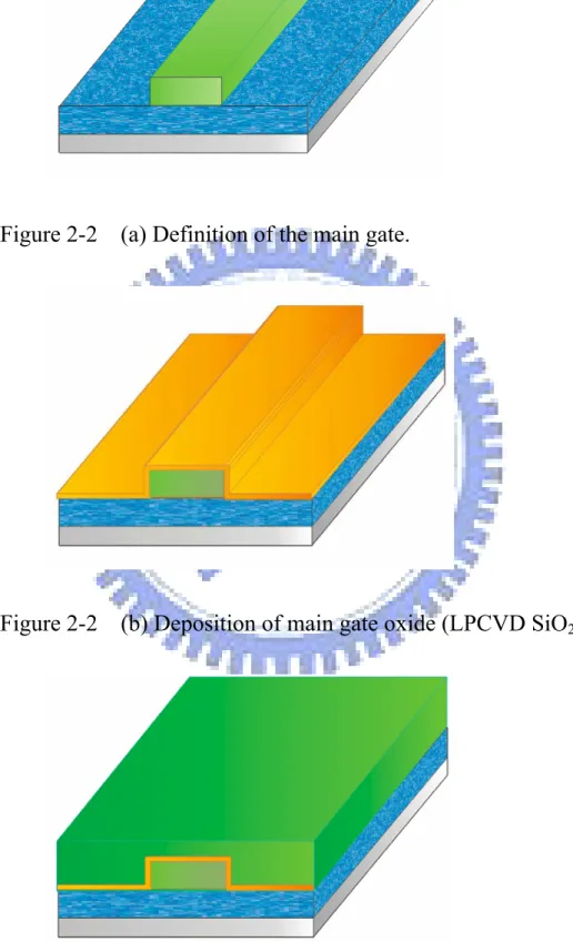
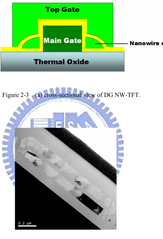
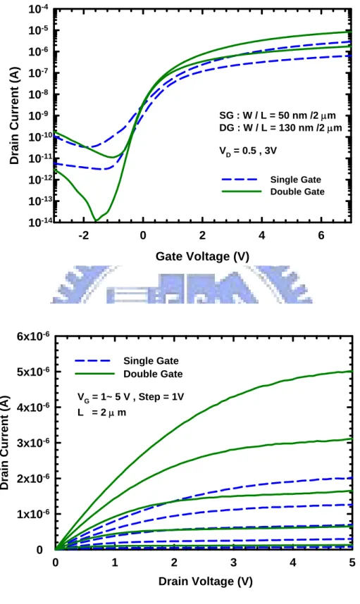
(11) nnnnnnnnnnnnnnnnnnnnnnn. Figure Captions. Figure 2-1 (a) Schematics of double-gated nanowire thin-film-transistor.. …..……….39 Figure 2-1 (b) Top view of double-gated nanowire thin-film-transistor………….…... 39 Figure 2-2 (a). Definition of the main gate………………………………………......…40. Figure 2-2 (b). Deposition of main gate oxide (LPCVD SiO2)……………...............…40. Figure 2-2 (c) Deposition of source/drain and channel layer……………...….....….…40 Figure.2-2.(d). After ion implantation,self-aligned formation of source /drain snanowire channel………………………....………………………….. 41. Figure 2-2 (e). Deposition of top gate oxide (LPCVD SiO2)……………......…………41. Figure 2-2 (f). Deposition and formation of top gate……………………………..……41. Figure 2-3 (a). cross-sectional view of DG NW-TFT…………………………..……...42. Figure 2-3 (b). TEM picture of cross-sectional view…………………..…..………..…42. Figure 2-4 (a). Parameter definition of DG NW-TFT………………..…..……...……..43. Figure 2-4 (b). TEM picture of DG NW-TFT………………………..……...…..……..43. Figure3-1.(a). Transfer characteristics of SG NW-TFTs and DG NW-TFTs with channel channel length of 2μm……………………………….…………………44. Figure3-1 (b). Output characteristics of SG NW-TFTs and DG NW-TFTs with nel channel length of 2μm ………………...….…………...………..….…..44. Figure3-2.(a) Transfer characteristics of DG NW-TFTs with channel length of 0.8mandk5μm……………………………………………...………….45 Figure3-2.(b) Output characteristics of DG NW-TFTs with channel length of 0.8 and 5 0.8aanda5μm ………………………………………..………..…..…...45. v.
(12) Figure3-3.(a). Transfer characteristics of a DG NW-TFT under TG and MG and DG andaDG mode……………………………………..…..…...………….46. Figure3-3.(b). Cross-section of a DG NW-TFT…………………...…..…...………….46. Figure3-4. Output characteristics of a DG NW-TFT under TG and MG and DG DGAmode .……………………………………………………...….…47. Figure.3-5.(a). Id-Vg characteristics of DG-NWTFT with 3hr NH3 plasma treatment time time by sweeping MG with Vtop gate from 3 to -3 V in step of 1V…..…48. Figure.3-5.(b). Id-Vg characteristics of DG-NWTFT with 3hr NH3 plasma treatment time time by sweeping TG with Vmain gate from 3 to -3 V in step of 1V….....48. Figure 3-6 (a). The MG mode (the top gate is grounded) threshold voltage as a function function of channel length for different top gate oxide thickness DG NW-TFT devices with VD = 0.5 V (Vth @ ID = 10-8 A)………….……49. Figure 3-6 (b). The TG mode (the main gate is grounded) threshold voltage as a function function of channel length for different top gate oxide thickness DG NW-TFT devices with VD = 0.5 V (Vth @ ID = 10-8 A)………….…….49. Figure 3-6 (c). The MG mode (the top gate is grounded) threshold voltage as a function function of channel length for different top gate oxide thickness DG NW-TFT devices with VD = 0.5 V (Vth @ ID = 10-8 A)………..…….50. Figure 3-7 (a). Transfer characteristics of DG-NWTFTs operate in TG mode (the main main gate is grounded) with different gate width…………….………..51. Figure 3-7 (b). Transfer characteristics of DG-NWTFTs operate in MG mode (the top top gate is grounded) with different gate width…………………….…51. Figure.3-7.(c). Transfer characteristics of DG-NWTFTs operate in DG mode with different gate width. ………………….…………………….……….. 52. Figure 3-8 (a) On-state drain current as a function of gate width……...……….……53 Figure.3-8.(b) Normalized drain current to Id (@ GW = 0.8μm) as a function of gate gate gate width……………………….…….….………………...…….…...53 vi.
(13) Figure.3-9.(a) Off-state leakage of DG-NWTFTs at 0.5V at various temperatures under TG under TG mode (the main gate is grounded)……..…………….…….54 Figure.3-9.(b) Off-state leakage of DG-NWTFTs at 0.5V at various temperatures under MG under MG mode (the top gate is grounded)………………….………54 Figure.3-9.(c) Off-state leakage of DG-NWTFTs at 0.5V at various temperatures under under DG mode……………………………………..………………..55 Figure 3-10. Activation energy of DG NW-TFTs with different gate width and gate gate gate voltage as a function of gate voltage……………………….…….56. Figure 3-11. Leakage mechanism in drain/channel junction (a) thermionic-emission (b) thermionic-field emission. (c) band-to-band tunneling…………..57 7 Figure 3-12 Leakage mechanism in gate-to-drain overlap region (a) thermionicemission (b) thermionic-field emission (c) band-to-band tunneling....58 g……...……………………………… Figure 3-13.(a) Off-state leakage of DG-NWTFTs at 0.5V at various channel lengths lengths under TG mode (the main gate is grounded)………………...59 Figure.3-13.(b) Off-state leakage of DG-NWTFTs at 0.5V at various channel lengths lengths under MG mode (the top gate is grounded)………………….59 Figure.3-13.(c). Off-state leakage of DG-NWTFTs at 0.5V at various channel lengths lengths under DG mode .……………………………………………..60. Figure 4-1(a) Transfer characteristics of DG NW-TFTs under different NH3- plasma treatment time. tox. top = 32nm………………………………………….61 Figure 4-1(b). Transfer characteristics of DG NW-TFTs under different NH3- plasma treatment time. tox. top = 18nm……………………………..….………..61. Figure 4-2. Transfer characteristics of DG NW-TFTs under different N2-plasma treatment time. tox. top = 32nm……………………………….…..……..62. Figure 4-3. Transfer characteristics of DG NW-TFTs under NH3 or N2 plasma treatment. tox. top = 32nm ……………………………………...…….62. Figure 4-4. Minimum drain current as a function of plasma treatment time. tox.top = . vii.
(14) tox.top = 32nm……………………………………………………..……63 Figure 4-5. Threshold voltage with as a function of plasma treatment time. Vth = Vg Vth = Vg @ ID = 10nA. tox. top = 32nm………………..…………….…...…..63. Figure 4-6 Transfer characteristics of metal-top-gate DG NW-TFTs under different NH3-plasma treatment time…………………..……………….……..……..64 Figure 4-7 Activation energies of DG NW-TFTs s a function of gate voltage for different plasma- treatment time…………………………………………..65 Figure 5-1 Schematic showing the stronger fringing field effect induced by the high-k high-k material in the nanowire channel………………………………….66 Figure 5-2 Transfer characteristics for the device without (i.e., SG NW-TFTs (A)) and and with high-k passivation (i.e., SG NW-TFTs (B))………….………..….66 Figure 5-3 Output characteristics for the device without (i.e., SG NW-TFTs (A)) and and with high-k passivation (i.e., SG NW-TFTs (B)).Vg ‘ = Vg – Vth........ 67 Figure.5-4.(a) Transfer characteristics of SG NW-TFTs without high-k passivation, measured at various temperatures………………………………..…….....68 Figure 5-4.(b) Transfer characteristics of SG NW-TFTs with high-k passivation, measured measured at various temperatures………………………………….……...68 Figure 5-5 Activation energy for the device without (i.e., SG NW-TFTs (A)) and with high-k passivation (i.e., SG NW-TFTs (B)), as a function of gate voltage...69. viii.
(15) Chapter 1 Introduction 1.1 Double-gated poly-Si TFTs Polycrystalline silicon (poly-Si) thin-film transistors (TFTs) have been studied for a long time for their applications to liquid crystal display [1], such as pixel switches, drivers, and peripheral control circuits in active-matrix liquid-crystal displays (AMLCDs) [2]. In recent years, Poly-Si TFTs have broaden their applications to memories and sensors, such as static radom access memories (SRAMs) [3] [4], electrical erasable programming read only memories (EEPROMs) [5], and image sensors [6]. For these applications, scaled-down poly-Si TFTs with high performance and high reliability are required. The electrical characteristics depend on the poly-Si quality and the transistor’s structure. Compared with amorphous silicon (a:Si) TFTs, poly-Si TFTs exhibit higher drive current [7] and mobility [8]. However, the performance of conventional poly-Si TFTs can not fully satisfy the requirements of these applications [9] [10] because of the presence of grain boundaries. Many pending issues remain to be resolved. For example, poly-Si TFTs normally depict anomalous off-state leakage current, which originates from the high electric field between the gate and drain [11] and the defects in grain boundaries (GBs) in the channel [12] [13]. It causes poor switching characteristics and limits their applications. Various solutions such as lightly-doped drain (LDD) poly-Si TFT [14] structure has been proposed to. 1.
(16) reduce the electric field between the gate and drain. Other structures, such as Schottky barrier thin-film transistors (SBTFT) with field induced drain (FID) [11], offset gate [15], the p-n-p gate [16] are also proposed to reduce the off-state leakage current. In addition, the grain size and grain quality in poly-Si channel material are known to greatly affect the electrical performance of poly-Si TFTs [17]. There are a lot of studies devoted to improving the channel material quality of poly-Si TFTs in order to obtain better device performance [18], [19]. Nowadays, several methods have been developed for improving the poly-Si material quality or growing poly-Si channel with single or few grain boundaries. For example, the solid phase crystallization (SPC) [20], [21] has been proposed to transfer amorphous Si into poly-Si with few defects by long time annealing. The metal-induced lateral crystallization (MILC) [22], [23] introduces metal as a crystal seed for lowering the crystallization temperature of a-Si to poly-Si with large grain size and few defects. Moreover, excimer laser crystallization (ELC) [24] and plasma treatment [25], [26] are also very useful methods to improve poly-Si channel quality. On the other hand, scaling down TFT can greatly improve the electrical performance. The smaller device size enables higher device density in SRAMs and DRAMs, and also increases the driving current of peripheral driver circuits in AMLCD applications. However, several short-channel effects are known to aggravate with reducing TFT dimension, such as threshold voltage roll-off, larger drain-induced barrier lowering (DIBL), and the kink-effect. Several multi-gate structures including double-gate [27], tri-gate [28], FinFET [29] and gate-all-around [30] CMOS technology have been proposed to improve the gate controllability over the channel, and therefore reduce short-channel effects. It has been experimentally demonstrated that the double-gated (DG) structure can provide a higher driving current because it has twice the conduction channel area 2.
(17) per device area [31]. Also, the better subthreshold slope is ascribed to the stronger control by the gate voltage on the channel potential [32]. The unique geometric structure can also suppress the short-channel effects [33], compared with single-gated TET. In addition, the use of an ultra thin silicon channel will ensure a tight coupling between the gate potential and the channel, thus reducing DIBL effect [34]. The most common operation mode of DG TFT is to bias a common gate by tying the two gates together. It can also be operated by having different biases on two gates simultaneously to flexibly control the threshold voltage of TFT [35]. As a result, the double-gated TFT is very attractive for both analog and digital applications.. 1.2 Overview of nanowire structures In order to have higher drain current, Ion/Ioff ratio, switching speed and aperture ratio, nanowire technology is crucial for scaled devices. TFT with its channel smaller than 100 nm is referred to as “nanowire device”, which has several unique features such as high surface-to-volume ratio, small size, and high surface sensitivity. Because of these advantages, silicon nanowires (SiNWs) [36] have superior electrical performance [37] and have been applied to many applications including switches [38], memories [39], [40], large-area electronics, and chemical and biological sensors [41]. Nowadays, the NWs can be prepared by either top-down [42], [43] or bottom-up approaches [44]. The top-down approaches typically need advanced lithography tools, such as e-beam, X ray, nano-imprint, etc. However, the advanced lithography tools are very expensive. For the bottom-up approaches, the metal-catalytic growth [45] and oxide-assisted catalyst-free method are usually employed [46]. The former approach is straight-forward for the fabrication of nanowire devices, but is costly. The latter approach, though less expensive, also possesses many problems, such as the 3.
(18) precise growth on the designed device location and metal contamination, etc. In this study, to circumvent these shortcomings, we develop a simple method for the preparation of Si nanowire TFT double-gated devices.. 1.3 Plasma treatments on poly-Si Grain boundaries and in-grain defects of poly-Si film as a result of the limitation of deposition condition result in the continuous distribution of traps in the forbidden bandgap [47], which will degrade the carrier transport and device electrical performance. The variation of threshold voltage and subthreshold slope of TFTs is associated with the deep states originated from the dangling bonds of grain boundaries. The mobility and minimum leakage current are associated with the tail states originated from the in-grain defects [48]. The density of in-grain defects of poly-Si film transformed from amorphous silicon by low-temperature solid-phase crystallization (SPC) is very high. These trap states can be passivated by hydrogen, but high hydrogen concentration and long treatment time are needed for its accumulation. Among various hydrogenation methods, the hydrogen plasma treatment [49] and hydrogen implantation [50] are the two most common methods. The hydrogenation tends to tie up the grain-boundary dangling bonds and improves the characteristics of poly-Si TFTs [51]. However, the weak Si-H bond is unstable at temperature higher than 400oC, and suffers from poor hot-carrier endurance [52]. Other plasma gases like NH3, N2, O2, N2O, CF4 are also used [53] -[55]. Tsai et al. showed that the electrical characteristics of poly-Si TFTs were much improved using the H2/N2 mixture plasma treatment than the pure H2 plasma treatment [56]. It is attributed to the nitrogen passivation and the promotion of hydrogen plasma generation by nitrogen radical collision. Yang et al. also showed that the 4.
(19) characteristics of poly-Si TFTs can be improved by combining the nitrogen implantation and the H2-plasma passivation [57]. Defects passivation of nitrogen could be responsible for the improved characteristics. On the other hand, it has also been proposed that NH3 plasma treatment can improve hot-carrier reliability, compared with pure H2 plasma. It is attributed to the nitrogen pile-up at SiO2/poly-Si interface and the formation of strong Si-N bond that will terminate the dangling bonds at the grain boundaries of the polySi films. [58]. 1.4 Motivation As mentioned above, the simple and low-cost top-down approach is an attractive way to fabricate nanowire devices. Recently, our laboratory proposed and demonstrated a novel and cost-effective method (i.e., no need of costly lithographic instruments) to fabricate NW DG-TFTs [59]. We have successfully fabricated nanowire poly-Si channel by borrowing the concept of the sidewall spacer formation in MOSFET. The advantages of our process are as follows. (1) It is a simple low-temperature process. (2) It is a low-cost process. It does not require costly advanced lithography tool or expensive SOI wafers. (3) The technique has strong flexibility and can be readily extended from silicon to strain silicon, silicon germanium, and germanium. (4) It is compatible with modern semiconductor processes. However, the gate controllability of the second gate is weak because of the thick gate oxide. In my thesis, a very thin gate oxide was tried to improve the second gate controllability. Moreover, the high k stacked layers of Al2O3 and HfO2 were used to 5.
(20) cap the top of the SG NW-TFT channel to study the effect of high-k gate oxide on the electrical performance. From the mechanisms discussed above, NH3 and N2 plasma treatments were explored to improve the electrical characteristics of DG NW-TFTs in our study.. 1.5 Thesis organization. In this thesis, we have fabricated double-gated nanowire thin film transistors and single-gated nanowire thin film transistor with high-k passivation layer. The overviews of double-gated poly-Si TFTs, nanowire channel, and plasma treatments are introduced in Chapter 1. In Chapter 2, we introduce the device fabrication process and the measurement parameters. Chapter 3 discusses the electrical characteristics of double-gated devices. Three operation modes, namely, TG mode (i.e., bias applied to the top gate with grounded main gate), MG mode (i.e.,bias applied to the main gate with grounded top gate,) and DG mode (i.e., bias applied to the main gate and top gate simultaneously) were discuss carefully in Section 3.1. And the leakage mechanism of DG NW-TFT was investigated in Section 3.2. In Chapter 4, we explore methods to improve the device performance by subjecting the device to different plasma treatment, and their mechanisms are discussed. In Chapter 5, we study the fringing field effect of the high-k passivation on SG NW-TFTs. Finally, we summarize the conclusions, and future works are suggested in Chapter 6.. 6.
(21) Chapter 2 Device Fabrication and Measurements 2-1 Device Structure and Fabrication The structure and top view of double-gated dual-channel thin film transistor is shown in Figs. 2-1(a) and (b). 6 inches n-type Si wafers were used as the starting substrate. First, a150nm SiO2 layer was grown by thermal oxidization on Si wafer. Then, n+-doped poly-Si layer of 100nm was grown to serve as the main gate. SiO2 dielectric with a thickness of 18 and 36 and 67 nm was grown, respectively, on polySi by low-pressure chemical vapor deposition (LPCVD) with TEOS as the source, to serve as the main gate oxide. An a-Si layer was then deposited by LPCVD at 550 oC, followed by a thermal annealing at 600 oC in N2 ambient for 24 hours to transform aSi into poly-Si (i.e., solid phase crystallization process). P31+ ion implantation with a dose of 1 x 1015 cm-2 at 15 keV was performed and the source/drain (S/D) regions were defined by a standard lithography. It should be noted that the implant energy was kept low so that the implanted dopants were distributed near the top surface of the poly-Si layer. The S/D photoresist patterns were then formed by a standard lithography. Afterwards, a reactive plasma etching was used to remove the poly-Si layer without the photoresist protection and two Si channel nanowires were formed in a self-aligned manner. Since the implantation energy is low, the dopants in places other than S/D regions were removed during the reactive plasma etching owing to the shallow projection range. The S/D dopants were activated by annealing treatment at 600 oC for 30 min. Then, an LPCVD SiO2 thickness of 18 and 32 and 60 nm, 7.
(22) respectively, was deposited to serve as the top gate oxide. A 100 nm in-situ-doped ntype poly-Si was then deposited and patterned to serve as the top gate. Finally, a 200nm SiO2 passivation oxide was deposited. The standard metallization process was used for the formation of metal pads. Both NH3-plasma and N2-plasma were used to improve the device characteristics. A parallel-plate plasma reactor with RF power of 200 W, flow rate of 700 sccm for NH3-plasma and 300 W, 200 sccm for N2-plasma were used, and the treatment temperature was fixed at 300 oC. The treatment time was varied to serve a process parameter in this study. The process flow-charts are illustrated in Figs. 2-2 (a) to (f). The fabrication process of nanowire TFT with high-k passivation was the same as the process shown in Figs. 2-2 (a) to (d), except that the main gate oxide thickness was kept at 15nm. The high-k passivation of 10nm Al2O3 and 20nm HfO2 prepared by MOCVD was finally capped with 200nm SiO2 passivation. The cross-sectional view of DG NW-TFT is shown in Fig. 2-3(a), while the images by transmission electron microscopy (TEM) after device formation is shown in Fig. 2-3(b). Figure 2-4 (a) defines the device parameters of DG NW-TFT, and the TEM picture is shown in Figure 2-4 (b). The width and thickness of NW channel are 50 and 80nm, respectively.. 2-2. Device. characteristics. and. measurements. of. nanowire thin-film transistors. The electrical performance of TFTs strongly depends on its structure and the channel quality. There are several important parameters, namely, top gate oxide. 8.
(23) thickness (tox,top), main gate oxide thickeness (tox,main), channel length (L) and gate width (GW). The channel structure depends on the geometry of main gate height and oxide thickness, and the channel size can be controlled by the over-etching time during the channel fabrication process. Current–voltage (I–V) characteristics were characterized by an HP 4156 semiconductor parameter analyzer at a stable temperature controlled by temperatureregulated hot chuck. I-V characteristics of transistors including threshold voltage (Vth) and subthreshold swing (SS) were measured and derived using an HP4156 parameter analyzer. From the ID-VG curve at VG = 0.5 V, the characteristics of DG NW-TFTs including threshold voltage (Vth), subthreshold swing (SS), field-effect mobility (μFE) can be extracted according to their definition. The threshold voltage is defined as the gate voltage (VG) to achieve a drain current (ID) of (W/L)×100 nA, i.e., Vth is extracted approximately at ID = 10 nA.. Vth = VG @ I D =. W ×100nA L. (2-1). where W and L are the channel width and length, respectively. The subthreshold swing (SS) can be calculated from the subthreshold current in the weak inversion region by. SS =. ∂VG ∂VG ∂VG = (log 10) = 2 .3 ∂ (logI D ) ∂ (logI D ) ∂ (logI D ). (2-2). Finally, the field-effect mobility (μFE) is determined by. μ FE =. Lg m WCox VD. (2-3). where gm is the maximum transconductance and Cox is the gate capacitance per unit area.. 9.
(24) The transconductance, GM, is extracted by the differentiation of ID to VG.. GM =. ∂I D ∂ VG. ⎛W ⎞ = V D = const ⎜ ⎟ μ C OX V D ⎝ L ⎠. 10. (2-4).
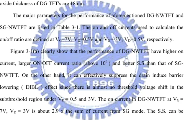
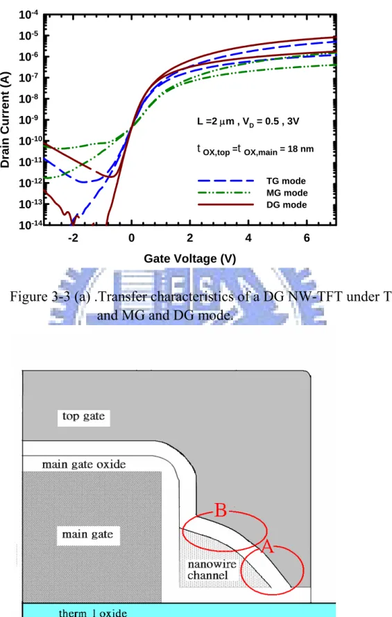
(25) Chapter 3 Poly-Si Nanowire Thin-Film Transistors With Double Gated Structure. From our previous studies, we demonstrated a novel method to develop poly-Si nanowire thin film transistors with very simple and non-expensive procedure. The nanowire thin film transistors (NW-TFTs) offer unique characteristics of lower leakage current, higher carrier mobility and better sub-threshold slope due to the inherent large surface-to-volume ratio, small volume of nanowire, fewer defects and grain boundaries existed in poly-Si nanowires. The stronger gate control can result in the suppression of undesirable short channel effects. In addition, we can improve the characteristics of NWTFTs with the ammonia (NH3) plasma treatment. In this work, we study the characteristics improvement of this device with an additional top polygate on the original main-gate, which is so called a double-gate nanowire thin film transistor (DG-NWTFT), to offer better performance including higher ON current, larger ON/OFF current ratio, and steeper subthreshold slope (S.S.) due to the additional stronger gate control. In order to further understand the electrical characteristics of DG-NWTFT, the comparison of the SG-NWTFT and DG-NWTFT, the gate oxide thickness, the gate width and the off state leakage mechanism will be studied carefully in this chapter.. 11.
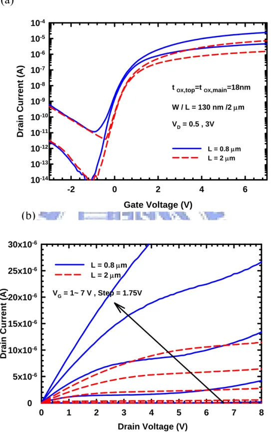
(26) 3.1 Electrical characteristics of NW-DG TFTs. vFrom Fig. 2-4 (b), the conduction channel width of about 50nm and 80nm were effectively controlled by the main-gate and the top-gate, respectively, and hence the total channel width under double-gate control mode is 130nm. The ID-VG and ID-VD characteristics of the NW-TFTs in (single-gate) SG and (double-gate) DG devices after 3-hour plasma treatment in NH3 ambient are shown in Fig. 3-1(a) and Fig. 3-1(b). The gate oxide thickness of SG-NWTFT's is 18 nm and both the main gate and top oxide thickness of DG TFT's are 18 nm. The major parameters for the performance of aforementioned DG-NWTFT and SG-NWTFT are listed in Table 3-1. The on and off currents used to calculate the on/off ratio are defined at VG=7V, VD=0.5V and VG=-3V, VD=0.5V, respectively. Figure 3-1(a) clearly show that the performance of DG-NWTFT have higher on current, larger ON/OFF current ratio (above 106 ) and better S.S than that of SGNWTFT. On the other hand, it can effectively suppress the drain induce barrier lowering ( DIBL ) effect since there is almost no threshold voltage shift in the subthreshold region under VD = 0.5 and 3V. The on current in DG-NWTFT at VG = 7V, VD = 3V is about 2.9 x the sum of current from SG mode. The S.S. can be reduced from 360 mv/dec to 180 mv/dec. From the ratio of ON-current to channel width, the current per unit channel width of DG-NWTFT is 32 μA/μm (8.4μA/260μm), which is similar to that of SG one 29 μA/μm (2.9μA/100μm). It implies that the conduction path of NW device is via the channel surface instead of the bulk. It can be observed clearly that the DG device has higher ON current and steeper S.S. and better gate controllability to suppress the DIBL effect than that of SG NWTFTs in Fig. 3-1(a) and (b). The mechanisms are (1) the improvement of the 12.
(27) subthreshold slope to suppress the DIBL effect of DG device is attributed to the stronger control of the gate voltage on the channel potential in the DG structure. (2) the increase of the on current is from two conducting area and the mutual modulation effect of the double-gates (3) the increase in the effective mobility may come from the lower average vertical electric field in the channel, which reduces the interface roughness scattering [60]. Although these advantages mention above, there is one point we have to pay attention. The off current of DG-NWTFT operated at VG=-3V, VD=3V is higher than that of SG-NWTFT, which is from the gate-induced drain leakage (GIDL) effect [61] [62]. It needs further improvement. In Fig. 3-2(a) and Fig. 3-2(b), the influence of channel length in DG-NWTFTs is also investigated. Figure 3-2(a) depicts the transfer characteristics of DG-NWTFT with the channel length of 0.8 and 2.0μm. It was reasonable to show that when the channel length is shorter, the drain current is higher. It can be summarized that the DG device has better controllability, so the drain-induced-barrier-lowing (DIBL) effect is not observed even in short channel devices. As shown in Fig. 3-2(b), the drain current for the DG-NWTFT device with the shorter channel length of 0.8 μm can not saturate. The electric field increases with decreasing the channel length under a fixed drain voltage. As the drain voltage is 8V, the drain current is much increased. The electric field in the channel is 8V/0.8μm = 1 x 10⁵ V/cm, which is too small to induce ionization [63]. It is from the DIBL and threshold-voltage-roll-off effects. The gate controllability in short channel devices is degraded by the electric field of drain, which can be easily observed in output characteristics of Fig. 3-2(b). It is also observed the saturation of drain current is difficult for the shorter channel device with L = 0.8μm.. 13.
(28) Figure 3-3 (a) shows the transfer characteristics and Figure 3-4 shows the output characteristics of DG-NWTFT device operated in SG and DG modes. For SG mode, when the device operated with the main gate grounded and the top gate as the control gate is denoted as TG, and when the device operated with the top gate grounded and the main gate as the control gate is denoted as MG. For DG mode, both top and main gates are connected together to serve as the control gate. From TEM examination, we observe that the conducting area of MG is about 60% that of TG. The ON saturation current of TG higher than that of MG is from the conducting area of TG larger than that of MG. It also means the minimum leakage current of MG should be lower than that of TG, but the fact is that the minimum leakage current of TG is lower than that of MG. It could be from our special geometric structure as shown in Fig. 3-3 (b). Because the top gate has higher controllability than that of the main gate, the channel below the top gate is in the depletion state or weak inversion state when the top gate is grounded. The channel below the main gate is in the accumulation state even with a negative voltage is applied on the main gate and also effect the channel energy band of region B (in Fig. 3-3 (b)) to be less depleted. But the region A (in Fig. 3-3 (b)) stays in the depletion state or weak inversion state. It should be noted that the larger OFF-current could be from the gate-induced drain leakage (GIDL) effect. The leakage mechanism will be carefully analyzed in the following section. From the results of Fig. 3-4 (a) and (b), they support the mechanism discussed above. Fig. 3-4 (a) shows the Id –Vg (top gate) with the main gate voltage as a parameter varied from 3 V to -3 V in a step of 1 V, and Fig. 3-4 (b) shows the Id –Vg. (main gate). with the top gate voltage as a parameter varied from 3 V to -3 V in a step of 1 V. In Fig. 3-4 (a) for the main gate is in off state, the drain current at fixed top gate voltage of 3V increases with the main gate voltage. It comes from the channel potential under 14.
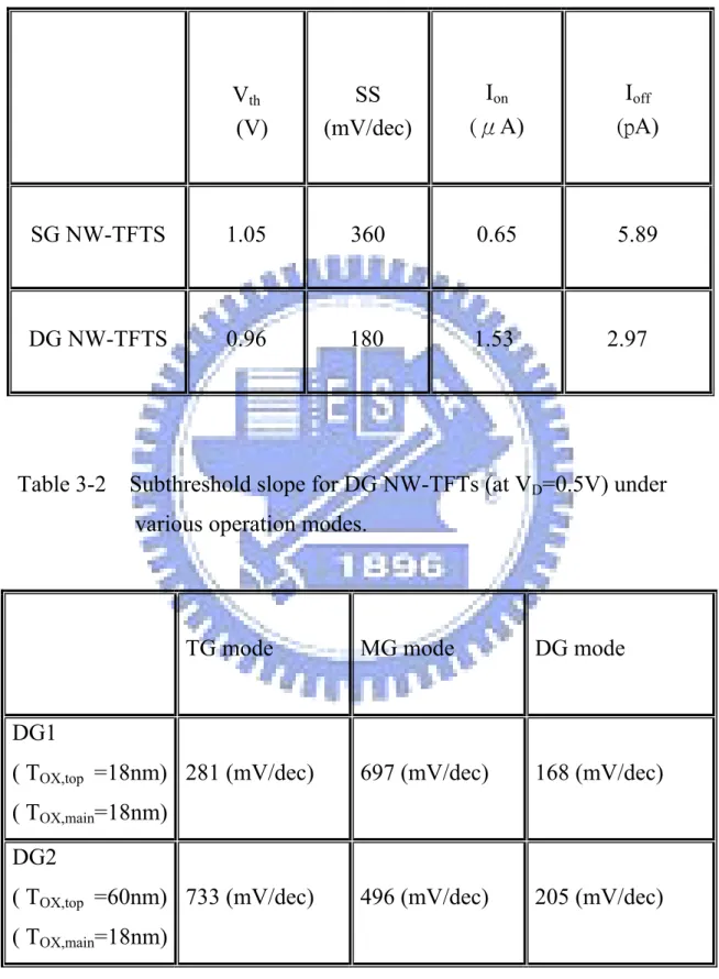
(29) the main gate will be raised by the top gate for nanowire channel [64] Owing to the high surface to volume ratio of NW structure, the channel potential is sensitive to both gates due to the floating body. From Fig. 2-3 (a), it can also be observed that a strong gate-to-gate coupling phenomenon on the corner due to the geometry. Based on two factors proposed above, the Vth (defined as the gate voltage as the drain current is 10 nA) of one transistor can be easily modulated by the gate voltage of the other one. For Vg,main applied to the main gate lower than 0 V, it should be noted in Fig. 3-4 (a) that Id-Vg,top curve for DG-NWTFT hardly shifts. In this state, the main gate side surface potential is in accumulation, and is pinned regardless of Vg,main. For the same range of Vg,top applied to top gate, the curve shift phenomena in Fig. 3-4 (b) is similar to that in Fig. 3-4 (a), but with larger shift. It is attributed the special geometry of our device structure. In order to understand the mutual interaction of TG and MG in DG-NWTFT, the DG-NWTFTs with different gate oxide thicknesses were studied and their threshold voltage as a function of channel length under different operation mode are shown in Fig. 3-6 (a), (b) and (c). DG1 and DG2 represent the DG devices with the top-gate oxide thicknesses of 18nm and 60 nm and the main-gate oxide thickness is fixed at 18 nm. In Fig. 3-6 (a), the threshold voltage of MG mode (the top gate is grounded) of DG2 is lower than that of MG mode of DG1. It is from that the effective positive oxide charge density is higher for thicker gate oxide and induces wider depletion region under the grounded top gate, the threshold voltage of MG mode of DG2 can be lower due to the contribution of the wider depletion region induced by the top gate on the corner interaction region. In Fig. 3-6 (b), it can be observed that when DG1 and DG2 operated in TG mode (the main gate is grounded), the Vth roll-off phenomena of DG2 is obvious as the channel length shorter than 2 μm. Because the thicknesses of 15.
(30) top-gate oxide of DG2 is about 2 times of DG1 and results in a lower electrical potential in the channel of DG2, and the electrical potential barrier can be more easily lowered by the drain voltage potential, i.e., DIBL effect. From Fig. 3-6 (c), we can observe that the Vth roll-off for DG mode is more effectively suppressed than that of TG and MG modes. Because the electrical potential at the corner interaction region in the channels under two gates is much higher, it needs higher drain voltage for the potential barrier lowing for the Vth rolloff. In Table 3-2 show the subthreshold slopes of TG, MG and DG modes of the devices mention above (DG1 and DG2). Under the operation of MG mode, although with the top gate grounded and the same main gate oxide thickness of DG1 and DG2, it can be observed that the subthreshold slope of DG2 is much stepper than that of DG1. It is from that the thicker top gate oxide thickness of DG2 weakens the controllability from the top gate to the channel, so it is much easier for DG2 to turn on than of DG.. 3.2 Mechanisms of leakage current of NW-DG TFTs. The off-state leakage current is a very important issue in poly-Si TFT, and it will reduce the drain current ON/OFF ratio and consume extra power. There are may causes for the off-state leakage current. In our poly-Si TFTs, the off-state leakage current is mainly from the defects and traps in the in-grain and grain boundaries of polycrystalline silicon channel. Besides, the defects at the interface of Si/SiO2 resulted from the etching damage by TCP will contribute extra leakage current. In this section, we concentrate the leakage current induced from GIDL effect.. 16.
(31) Due to the small cross-section area of nanowire channel, the total off-state leakage current should be low. However, the off-state leakage current shown in Fig. 31 is not so low as our expectation and it shows strong dependence on the voltage difference between the gate and the drain. It might be associated with the electric field in the channel near the drain. Figure 3-7 (a), (b) and (c) show that the off-state leakage currents operated in TG (main gate grounded), MG (top gate grounded) and DG modes of DG-NWTFTs with various gate widths, 2μm channel length and 18 nm thickness of main and top gate oxide after 5 hours NH3 plasma treatment. The “gate width (GW)” is defined in Fig. 2-4 (a) as the width of the gate, not equal to the channel width. The drain current as a function of the gate width is shown in Fig. 3-8 (a). The normalized drain current to Id (@ GW = 0.8μm) is shown in Fig. 3-8 (b), it revels that the off-state leakage current at Vg = - 5 V in MG and TG modes is linearly proportional to the GW size, but the proportional constant is one only for the MG mode. So we can propose that the mechanism of the off-state leakage current for MG and TG modes are not completely the same. In the off-state, if the generation and recombination centers resulted from the traps distributed in the in-grain and grain boundaries is responsible for the leakage current. The activation energy of the traps is a fixed value. The activation energies under each bias condition are extracted by fitting the slope of Arrhenious plot by the following equation [66].. I OFF = I 0 exp(−. EA ) kT. (Eq. 3-1). I o = constant independent of temperature,. 17.
(32) Ea = drain current activation energy which measures the difference between the valence band edge and the energy of the grain boundary states within kT of the Fermi level.. And IOFF ,k, and T represent the off-state leakage current , Boltzmann constant, and temperature, respectively. The derived activation energy depends on the difference between gate and drain as shown in Fig. 3-10. It excludes the possibility that the leakage is from the defects. The Id-Vg characteristics measured at the temperatures ranging from 25OC to 125OC are shown in Fig. 3-9 (a), (b) and (c). The activation energies for devices with the gate widths of 0.8 and 5 μm are shown in Fig. 3-10. It can be observed that the activation energy operated in MG mode is essentially independent of the gate width and depends on the difference between drain and gate bias. It indicates that the leakage mechanism is not related to the defects, it could be related to the electric field in the channel between gate and drain From Fig.3-9 (b) and Fig.3-10 the difference of the off-state current operated in main gate mode is mainly dependent on the overlap area between the main gate and drain region (the red dashed line indicated in Fig. 2-1 (b) and magnitude gate and drain biases. However, the overlap area is the same for all NW devices. Therefore, the Gate-induced drain leakage (GIDL) is the most likely cause for the anomalously high off-state current. There are two possible regions for the off-state leakage generation in DG NW-TFTs, one is in the drain/channel junction and the other is in the gate-todrain overlap region, illustrated in Fig. 3-11 (a), (b), (c) and Fig. 3-12 (a), (b), (c) as follows [65]. For the drain/channel junction, there are generally three cases in Figs. 311 (a), (b) and (c):. 18.
(33) 1) In low electric-field regime: The off-state current is mainly dominated by thermal emission. At first, electrons are thermally excited from the valence band into the midgap traps of grain boundaries and then jumped into the conduction band. In this case, the activation energy is about half of the bandgap as shown in Fig. 3-11 (a). 2) In medium electric-field regime: The electrons are thermally excited from the valence band to the traps or surface states in the band gap and then tunneling into the conduction band, as shown in Fig. 3-11 (b). This is known as the thermionic-field emission. 3) In high electric-field regime: The band diagram is bent seriously under high electric field. The electrons are tunneling from the valence band directly into the conduction band. The quasi-Fermi level at the channel/oxide interface shifts nearer to the valence-band edge, and the band-to-band tunneling easily happened with the aid of trap states, and lead to high leakage current in the off-state region as shown in F Fig. 3-11 (c). This is known as the band-toband tunneling. It takes place near the drain region instead of tunneling through the gate oxide, which is known as the gate-induced drain leakage (GIDL).. For the gate-to-drain overlap region, the leakage current depends on the width of the gate and the magnitude of drain bias. There are also three cases depending on the electric field strength in the gate-to-drain overlap region as illustrated in Figs. 3-12(a), (b) and (c), which are similar to that of the drain/channel junction. The GIDL current is resulted from the high electric field existed at the oxide/drain region under the high bias of VGD, which will result in a depletion region in the drain region and eventually leads to the band-to-band or trap-assisted tunneling process in 19.
(34) the depletion region. The origin of the GIDL effect in the NW devices comes from the doping profile in the drain. In our fabrication process, the low energy (e.g.,15 keV) implantation for S/D formation was used to avoid excessive dopant incorporation in the NW channels. This results in a gradient doping profile and the doping concentration decreases toward the oxide/Si interface. This will enhance the GIDL current in the OFF state. The off-state leakage currents of DG NW-TFTs with the same gate width and various channel lengths are shown in Fig. 3-13 (a), (b) and (c), after 4-hour plasma treatment in NH3 ambient. When the channel length is longer than 2 μm, the off-state currents in TG mode is strongly dependent on the channel length, but it is independent in MG mode. From Fig. 3-7 (a) and 3-13 (a),it can be observed clearly that there is still another factor contributing TG mode off-state leakage current besides the GIDL effect.. 20.
(35) Chapter 4 Plasma Treatment Effects on Nanowire Double-Gated Thin-Film Transistors. In Poly-Si TFTs, the SiO2/Si interface, grain boundaries, and in-grain defects play crucial roles in the device performance. It is well known that the quality of PolySi TFTs can be improved with plasma-treatment by passivating the dangling bonds associated with SiO2/Si interface, grain boundaries and the in-grain defects. Many gases including NH3, N2, O2, N2O, CF4 were used for plasma treatment [53]-[55]. In general, the H2 plasma treatment is very effective and common for passivation. However, it is not stable because of its weak Si-H bonds. On the other hand, the NH3 plasma treatment is attractive, as it not only offers the good feature of H2 plasma but also provides the pile-up of nitrogen at oxide/poly-Si interface and forms strong Si-N bonds to alleviate the hot carrier issue and achieve better device performance. The pure N2 plasma passivation is also promising, as it also forms strong Si-N bonds. In the past, the effect of plasma treatment on poly-Si TFT had been widely discussed. However, its effects on the nanowire device has yet to be clarified. In this work, both NH3 and N2 plasma treatments were employed and the passivation mechanisms were discussed.. 21.
(36) 4.1 Electrical characteristics of NW-DG TFTs with plasma treatment. The Id-Vg characteristics of DG-NWTFT with a gate oxide thickness of 32 nm under various NH3-plasma treatment times ranging from 0 to 5 hr are shown in Fig. 41(a). It can be seen that the drain current (@Vg=7v) increases, saturates gradually, and then decreases with the NH3-plasma treatment time, as shown in Fig. 4-1 (a). The maximum drain current can reach about 6.2 µA at a treatment time of 4 hr. The H and N ions exist in NH3-plasma treatment. The drain current increase is ascribed to the N and H passivation of defects in the gate oxide, the interface, and poly-Si of channels. As shown in Fig. 4-1(b), transfer characteristics of DG-NWTFT with a thinner gate oxide thickness of 18 nm under various NH3-plasma treatment times show similar trends, albeit it reaches the final stable state in a shorter NH3-plasma treatment time. From a previous study, the drain current is only marginally improved under H2 plasma treatment [49]. Id-Vg characteristics of DG-NWTFT with a gate oxide thickness of 32 nm under various N2-plasma treatment times ranging from 0 to 1 hr are shown in Fig. 4-2. We can see that the drain current increases and saturates gradually with the N2-plasma treatment time. The comparison of NH3 and N2 plasma treatments as show in Fig. 4-3. It can be seen that the subthreshold slope and the minimum current are better for N2 plasma treatment than for NH3 plasma treatment, given the same treatment time. It indicates that the passivation effect of N is stronger than that of H. When the plasma treatment time increases, more H and N ions diffuse into the device active region and the electrical performance is improved. Figure 4-4 shows that the minimum drain current increases initially, and then decreases with the NH322.
(37) plasma treatment time. The increase of minimum drain current when the treatment time is shorter than 2 hr is ascribed mainly to the radiation damage. While the decrease of minimum drain current when the treatment time is longer than 2 hr is ascribed mainly to the defect passivation effect of N and H in the gate oxide, the interface between gate oxide and poly-Si, and poly-Si, or the accumulated hydrogen passivation of poly-Si grain boundary, thus reducing the GIDL effect as proposed in our previous study. [67] For poly-Si-top-gate DG NW-TFT, the threshold voltage shifts toward left and then back to right with NH3-plasma treatment time, as shown in Fig. 4-5. The shift of threshold voltage toward left is from the generation of positive oxide-trapped charges induced by the plasma radiation damage. The positive oxide-trapped charges are distributed in the oxide, grain boundary and in-grain. The positive oxide-trapped charges in the grain boundaries can be reduced by H passivation. However, it takes much longer to reduce the defects inside the grains [48]. It is explained by the slowly moving back to right of threshold voltage shift with the treatment time. The slow recovery rate is dominated by the slow H diffusion rate in grain. In addition, the N accumulation at the SiO2/poly-Si interface could also contribute to the right shift of Vth. The dangling bonds at the SiO2/poly-Si interface can be effectively passivated by the strong Si-N bonds. From a previous study, the N atoms can even diffuse throughout the channel polysilicon region and passivate the in-grain defects [53]. The Si-N bonds can also increase the dielectric constant, which can enhance Id and in turn lower Vth.. 23.
(38) 4.2 Plasma treatment on metal-top-gate DG NW-TFTs Poly-Si DG-NWTFTs show large left-shift of Vth with a short (i.e., 0 to 2 hours) plasma treatment, possibly relating to radiation damage. This hypothesis is supported by the behavior of metal-top-gate (Al) DG-NWTFTs with poly-Si main gate, as shown Fig. 4-6, as the metal gate can effectively prevent the radiation damage. For metal-top-gate (Al) DG-NWTFTs with poly-Si main gate, the drain current as a function of gate voltage, with NH3-plasma treatment time as a parameter, is shown in Fig. 4-6. It can be seen that the electrical characteristics are greatly improved. The difference in subthreshold slope, minimum drain current, off-state leakage current, and threshold voltage shift with different treatment time becomes smaller. The almost constant threshold voltage shift indicates that the plasma radiation damages are indeed greatly reduced by the use of Al top-gate.. 4.3 Activation energy of DG NW-TFTs with different plasma treatment time. 1. The value of the activation energy reflects the carrier transport barrier of the grain. boundary within the poly-Si channel. The value of activation energy for various treatment times is shown in Fig. 4-7. The extracted activation energy for plasmatreated samples is higher than that for fresh devices, which implies that the trap states in the channel are passivated by the plasma treatment, so the leakage current becomes more difficult to generate.. 24.
(39) Chapter 5 Poly-Si Nanowire Thin-Film Transistors with High-k Passivation Layer. In order to improve the SG NW-TFT electrical performance, the passivation layer of SiO2 (k = 3.9, 250nm) layer was replaced with a stack layers of Al2O3 (k = 9, 10nm)/HfO2 (k = 25, 20nm)/SiO2 (200nm) in this study. By capping a passivation layer with high k material on the nanowire channel, the associated fringing field helps induce an additional conductive inversion-layer in the nanowire channel, as shown in Fig. 5-1. Similar trend is also expected for DG NW-TFTs.. 5.1 Electrical characteristics of SG NW-DG TFTs with high-k passivation layer For brevity, the single-gated TFT with SiO2 passivation is denoted as NWTFT(A), and the device with high-k passivation is denoted as NW-TFT(B) in this study. As shown in Fig. 5-2 and Fig. 5-3, we can see that the transfer and output characteristics of NW-TFT (B) show better subthreshold slope, lower drain current in subthreshold region, lower minimum drain current, and higher drain current, compared with those of NW-TFT (A), both receiving 3 hr NH3 plasma treatment. The stronger coupling causes more barrier lowering near the drain, improving the DIBL 25.
(40) effect. On the other hand, the high-k passivation layer also results in a lower equivalent oxide thickness between the gate (without channel underneath) and the channel. It is similar to the device with surrounding-gate, and therefore showing higher drain current, as clearly observed in Fig. 5-3. As for the lower minimum drain current for NW-TFT(B), it could be ascribed to more N and H ions diffusing through high-k material into in-grain and grain boundaries, resulting in more effective passivation during NH3 plasma treatment.. 5.2 Activation Energies of SG NW-DGTFTs with. 1. High-k Passivation Layer The drain current as a function of gate voltage with the measurement temperature as a parameter for NW-TFT(A) and NW-TFT(B), after NH3 plasma treatment for 3 hours, are shown in Fig. 5-4 (a) and (b), respectively. The drain current increases with the measurement temperature for both devices, albeit the temperature dependence is much minor for NW-TFT(B). This could be ascribed to the higher poly-Si quality with lower defect density by the NH3 plasma treatment for 3 hours. The lower recombination centers from lower defect density will contribute to lower carrier concentration, making it insensitive to the temperature. The above argument is supported by Fig. 5-5, which shows the activation energies of NW-TFT(A) and NW-TFT(B) after NH3 plasma treatment for 3 hours. When the gate voltage is smaller than zero bias, the activation energy of NW-TFT(B) is lower than that of NW-TFT(A) and is independent of the drain voltage. It indicates that the channel quality of NW-TFT(B) is better than that of NW-TFT(A).. 26.
(41) Chapter 6 Conclusions and Future works 6.1 Conclusions In this thesis, TFT devices with double-gated nanowire channel structure (DG NW-TFTs) were fabricated and the mechanism for electrical conductance was studied. Our results indicate that DG NW-TFTs have better electrical performance over SG NW-TFTs, including higher ON current, larger ON/OFF current ratio, steeper subthreshold slope(S.S.) and lower minimum drain current. Our results also show that stronger gate controllability that effectively suppresses the DIBL effect and lowers the leakage current in subthreshold region is achievable by employing the doubled-gated structure. In addition, the resultant DG device can act as a functional device by applying independent biases to two gates simultaneously, thus allowing the flexibility to adjust the threshold voltage of the device. The single-gated nanowire TFT with high-k passivation was also discussed in this study. The Id-Vg characteristics show that the fringing field effect from the highk passivation layer can effectively improve the device performance, including steeper subthreshold slope, lower DIBL effect….etc. In this study, we also found that both NH3 and N2 plasma treatments can dramatically improve the electrical performance of nanowire devices. In addition, we also found that the treatment time needed for suitable performance improvement is shorter with N2 plasma treatment.. 27.
(42) 6.2 Future works In this thesis, we have explored various structural parameters of nanowire TFTs, such as single-gate, double-gate, gate oxide thickness, channel size, and passivation layer on the device performance. In order to further improve the device performance, the following works are suggested for future research: 1. Several papers showed that the crystallization methods like SPC, MILC, ELC can effectively improve poly-Si channel quality. In this thesis, we concentrated our efforts on the SPC method. Other methods, such as MILC and ELC can be tried to improve the channel quality of DG NW-TFT in the future. 2. High-k gate dielectric is attractive for high performance devices. It could reduce the EOT while maintaining a higher physical thickness, thus lowering the leakage current. In addition, TFTs with high-k gate dielectric can have higher driving current. We can replace SiO2 gate dielectric with high-k material to improve device performance in the future. 3. The off-state leakage current associated with GIDL originated from the lightly-doped gate/drain overlapped region is still an important issue in our device. In the future, we can add an additional SiN layer between the main gate and drain to lower the electrical field, therefore alleviating the GIDL offstate leakage current. 4. The plasma passivation mechanism on nanowire device warrants further discussion. In the future, physical and chemical analyses such as SIMS,ECSA,OES…. can be employed to study the detailed mechanism.. 28.
(43) References [1]. S. Morozumi, K. Oguchi, SYazawa, T. Kodaira, H. Ohshima, and T. Mano, “B/W and color LC video display addressed by poly-Si TFTs,” SID Dig., pp. 156, 1983.. [2]. Ali A. Orouji, M. Jagadesh Kumar, “Leakage current reduction Poly-Si TFTs for active matrix liquid crystal displays: A comprehensive study,” IEEE Trans. Device Mater. Rel ., vol. 6, no. 2, pp. 315-325, June. 2006.. [3]. M. Aoki, T. Hashimoto, T. Yamanaka, and T. Nagano, “Large 1/f noise in polysilicon TFT loads and its effects on the stability of SRAM cells,” J. Appl. Phys., vol. 35, pp. 838-841, Feb. 1996.. [4] T. Ootani et. al., “A 4-Mb CMOS SRAM with a PMOS thin-film-transistor load cell,” IEEE J. Solid-State Circuits, vol. 25, no. 4, pp. 1082-1092, Oct. 1990. [5]. N. D. Young, G. Harkin, R. M. Bunn, D. J. McCulloch, and I. D. French, “The fabrication and characterization of EEPROM arrays on glass using a low temperature poly-Si TFT process,” IEEE Trans. Electron Devices, vol. 43, no. 11, pp. 1930-1936, 1995.. [6]. T. Kaneko, Y. Hosokawa, M. Tadauchi, Y. Kita, and H. Andoh, “400 dpi integrated contact type linear image sensors with poly-Si TFTs analog readout circuits and dynamic shift registers,” IEEE Trans. Electron Devices, vol. 38, pp. 1086-1093, May. 1991.. [7]. A. G. Lewis et al., “Degradation of polysilicon TFT’s during dynamic stress,’’ in IEDM Tech. Dig., 1991, pp. 575-578.. [8] Tadashi Serikawa, Seiiti Shirai, Akio O, “Low temperature fabrication of highmobility kamoto, and Shiro Suyama, ”poly-Si TFT’s for large-area LCD’s,” IEEE Trans. Electron Devices, vol. 36, no. 9, pp. 1929-1933, Sep. 1989. 29.
(44) [9] J. Jang, J. Y. Oh, and S. K. Kim, “Electric-field-enhanced crystallization of amorphous silicon,” Nature, vol. 395, no. 6701, pp. 481-483, Oct. 1998. [10]LH.-L. Chen and C.-Y. Wu, “An analytical grain-barrier height model and its characterization for intrinsic poly-Si thin-film transistor,” IEEE Trans. Electron Devices, vol. 45, no. 10, pp. 2245-2247, Oct. 1998. [11] .Kuan-Lin Yeh, Horng-Chih Lin, Rou-Gu Huang, Ren-Wei Tsai, and Tiao-Yuan Huang, “Conduction mechanisms for off-state leakage current of Schottky barrier thin-film transistors,” Appl. Phys. Lett., vol. 83, pp. 635-637, July. 2001. [12] .Matsumura M, Oh CH. Advanced, “Passivation of grain boundaries in polycrystalline silicon” Thin Solid Films, vol. 337, pp. 123-128, Jan. 1999. [13].lC. H. Seager and D. S. Ginley, “Anomalous leakage current in LPCVD polysilicon MOSFETs,” Appl. Phys. Lett., vol. 34, pp. 337-340, March. 1979. [14]. Shengdong Zhang, Ruqi Han, Johnny K. O. Sin, and Mansun Chan, “Reduction of off-current in self-aligned double-gate” IEEE Trans. Electron Devices, vol. 49, no. 8, pp. 1490-1492, Aug. 2002. [15] Cheol-Min Park, Byung-Hyuk Min, Jae-Hong Jun, Juhn-Suk Yoo, Min-Koo Han, “Self-aligned offset gated poly-Si TFTs with a floating sub-gate” IEEE Trans. Electron Devices, vol. 18, no. 1, pp. 16-18, Sep. 1997. [16] B. Min, C. Park, and M. Han, “A novel polysilicon thin-film transistor with a pn-p structured gate electrode,” IEEE Electron Device Lett., vol. 17, no. 12, pp. 560-562, Dec. 1996. [17] Albert W. Wang, and Krishna C. Saraswat, “A strategy for modeling of variations due to grain size in Polycrystalline thin-film transistors,” IEEE Trans. Electron Device, vol. 47, no. 5, pp. 1035-1043, May. 2000. [18]. T. Sameshima, S. Usui and M. Sekiya, “XeCl excimer laser annealing used in. 30.
(45) the fabrication of poly-Si TFT’s” IEEE Electron Device Lett., vol. 7, no. 5, pp. 276-278, 1986. [19] R. B. Iverson, and R. Reif, “Recrystallization of amorphized polycrystalline silicon films on SiO2 : temperature dependence of the crystallization parameters,” J. Appl. Phys., vol. 62, no. 5, pp. 1675-1681, 1987. [20] .A. Mimura, N. Konishi, K. Ono, J. I. Ohwada, Y. Hosokawa, Y. A. Ono, T. Suzuki, K. Miyata, and H. Kawakami, “High performance low-temperature poly-Si n-channel TFTs for LCD,” IEEE Trans. Electron Devices, vol. 36, pp. 351-359, Feb. 1989. [21] .R. B. Iverson, and R. Reif, “Recrystallization of amorphized polycrystalline silicon films on SiO2: temperature dependence of the crystallization parameters,” J. Appl. Phys., vol. 62, no. 5, pp. 1675-1681, 1987. [22]..Darren Murley, Nigel Young, Michael Trainor, and David McCulloch, “An investigation of laser annealed and metal-induced crystallized polycrystalline silicon thin-film transistors,” IEEE Trans. Electron Devices, vol. 48, no. 6, pp.1145-1151, June. 2001. [23]..Mingxiang Wang, Zhiguo Meng, Yitshak Zohar, and Man Wong, “Metalinduced laterally crystallized polycrystalline silicon for integrated sensor applications,” IEEE Trans. Electron Devices, vol. 48, no. 4, pp. 794 - 800, Apr. 2001. [24] Yu-Ru Chen, Chien-Hung Chang and Long-Sun Chao, “Modeling and experimental analysis in excimer-laser crystallization of a-Si films,” Journal of Crystal Growth, vol. 303, pp. 199-202, May. 2007. [25] .H. N. Chern, C. L. Lee, and T. F. Lei, “The effects of H2-O2 plasma treatment on the characteristics of polysilicon thin-film transistors,” IEEE Trans. Electron Devices, vol. 40, pp. 2301-2306, Aug. 1993. 31.
(46) [26] N. H. Nickel, A. Yin, and S. J. Fonash, “Influence of hydrogen and oxygen plasma treatments on grain-boundary defects in polycrystalline silicon,” Appl. Phys. Lett., vol. 65, no. 24, pp. 3099-3101, Dec. 1994. [27] Yuan Taur, “An analytical solution to a double-gate MOSFET with undoped body,” IEEE Electron Device Lett., vol. 21, no. 5, pp. 245 -247, May. 2000. [28] B. S. Doyle, S. Datta, M. Doczy, S. Hareland, B. Jin, J. Kavalieros, T. Linton, A. Murthy, R. Rios, and R. Chau, “High performance fully-depleted tri-gate CMOS transistors,” IEEE Electron Device Lett., vol. 47, no. 12, pp. 2320- 2325 , Apr. 2000. [29] Digh Hisamoto, Wen-Chin Lee, Jakub Kedzierski, Hideki Takeuchi, Kazuya Asano, Charles Kuo, Erik Anderson, Tsu-Jae King, Jeffrey Bokor, and Chenming Hu, “FinFET - a self-aligned double-gate MOSFET scalable to 20 nm,” IEEE Trans. Electron Devices, vol. 47, no. 12, pp. 2320-2325 , Dec. 2000. [30] Jae Young Song, Woo Young Choi, Ju Hee Park, Jong Duk Lee, and ByungGook Park, “Design optimization of gate-all-around (GAA) MOSFETs,” IEEE Trans Nanotech., vol. 5, no. 3, pp. 186-191, May. 2006. [31] Shengdong Zhang, Ruqi Han, Johnny K. O. Sin, and Mansun Chan, “Reduction of off-current in self-aligned double-gate TFT with mask-free symmetric LDD,” IEEE Trans.Electron Devices, vol. 49, no. 8, pp. 1490–1492, August. 2002. [32] Shengdong Zhang, Ruqi Han, Johnny K. O. Sin, and Mansun Chan, “Implementation and characterization of self-aligned double-gate TFT with thin channel and thick source/drain,” IEEE Trans. Electron Devices, vol. 49, no. 5, pp. 718-724, May. 2002. [33] Shengdong Zhang, Ruqi Han, Johnny K. O. Sin, and Mansun Chan, “A selfaligned double gate polysilicon TFT Technology” IEEE Electron Device Lett., vol. 22, no. 11, pp. 530-532, Nov. 2001. 32.
(47) [34] .Keunwoo Kim, Jerry G. Fossum, and Ching-Te Chuang, “Physical compact model for threshold voltage in short-channel double-gate devices,” in Intl. Conf. on Simulation of Semiconductor Processes and Devices (SISPAD), pp. 223-226, 2003. [35] .H. R. farrah, and R.F. steinberg, “Analysis of double-gate transistor,” IEEE Trans. Electron Devices, vol. 14, no. 2, pp. 69-74, Feb.1967. [36] X. Duan, C. Niu, V. Sahi, J. Chen, J. W. Parce, S. Empedocles, and J. L.Goldman, “High-performance thin-film transistors using semiconductor nanowires and nanoribbons,” Nature, vol. 425, no. 6955, pp. 274-278, Sep. 2003. [37] .Horng-Chih Lin, Ming-Hsien Lee, Chun-Jung Su, and Shih-Wen Shen, “Fabrication and characterization of nanowire transistors with solid-phase crystallized poly-Si channels,” IEEE Trans. Electron Devices, vol. 53, no. 10, pp. 2471-2477, Oct. 2006. [38] .J. E. Jang, S. N. Cha, Y. Choi, T. B. Butler, D. J. Kang, and D. G. Hasko et al., “Nano electron mechanical DRAM for ultra-large-scale integration,” in IEDM Tech. Dig., 2005, pp. 269-272. [39] L. Risch, L. Dreekornfeld, J. Hartwich, F. Hofmann, J. Kretz, and M. Stadele, “Multi gate transistors and memory cells for future CMOS generation,” in Proc. Tech. Dig. IEEE Silicon Nanoelectronics. Workshop, 2004, pp. 1-2. [40] .Shih-Ching Chen et al., “Nonvolatile polycrystalline silicon thin-film-transistor memory with oxide/nitride/oxide stack gate dielectrics and nanowire channels,” Appl. Phys. Lett., vol. 90, pp. 122111, Mar. 2007. [41] Yi Cui, Qingqiao Wei, Hongkun Park, and Charles M. Lieber, “Nanowire nanosensors for highly sensitive and selective detection of biological and chemical species,” Science, vol. 293, pp.1289-1292, 2001.. 33.
(48) [42] .S. Ecoffey, M. Mazza, V. Pott, D. Bouvet, A. Schmid, and Y. Leblebici et al., “A new logic based on hybrid MOSFET-polysilicon nanowires,” in IEDM Tech. Dig., 2005, pp. 277-280. [43] .F. L. Yang et al., “5 nm-gate nanowire FinFET,” in VLSI Symp. Tech. Dig., .2004, pp. 196-197. [44] .K. Das, A. K. Chakraborty, M. L. Nanda Goswami, R. K. Shingha, and A. Dhar, K. S. Coleman, S. K. Ray, “Temperature dependent shape transformation of Ge nanostructures by the vapor-liquid-solid method,” J. Appl. Phys. vol. 101, pp. 074307, 2007. [45] D. Wang, Q. Wang, A. Javey, R. Tu, H. J. Dai, H. Kim, P. McIntyre, T. Krishnamohan, and K. C. Saraswat, “Germanium nanowire field-effect transistors with SiO2 and high- k HfO2 gate dielectrics,” Appl. Phys. Lett., vol. 83, pp. 2432-2434, 2003. [46] .N. Wang, Y. F. Zhang, Y. H. Tang, C. S. Lee, and S. T. Lee, “SiO2-enhanced synthesis of Si nanowires by laser ablation,” Appl. Phys. Lett., vol. 73, pp. 3902-3904, 1998. [47] .I.-W. Wu, A. G. Lewis, T. Y.Huang, and A.Chiang, “Effects of trap-state density reduction by plasma hydrogenation in low-temperature polysilicon TFT,” IEEE Electron Device Lett., vol. 10, no. 3, pp. 123-125, Mar. 1989. [48] .I.-W. Wu, T. Y. Huang, W. B. Jackson, A. G. Lewis, and A. Chiang, “Passivation kinetics of two types of defects in polysilicon TFT by plasma hydrogenation,” IEEE Electron Device Lett., vol. 12, no. 4, pp. 181-183, Apr. 1991.. 34.
數據

+7
相關文件
– Factorization is “harder than” calculating Euler’s phi function (see Lemma 51 on p. 404).. – So factorization is harder than calculating Euler’s phi function, which is
“hard-wired” into the server code; instead, UDPServer determines the client port number by unraveling the datagram it receives from the client (using the .getPort() method). Thus
在1980年代,非晶矽是唯一商業化的薄膜型太 陽能電池材料。非晶矽的優點在於對於可見光
S15 Expectation value of the total spin-squared operator h ˆ S 2 i for the ground state of cationic n-PP as a function of the chain length, calculated using KS-DFT with various
雙極性接面電晶體(bipolar junction transistor, BJT) 場效電晶體(field effect transistor, FET).
Experiment a little with the Hello program. It will say that it has no clue what you mean by ouch. The exact wording of the error message is dependent on the compiler, but it might
[This function is named after the electrical engineer Oliver Heaviside (1850–1925) and can be used to describe an electric current that is switched on at time t = 0.] Its graph
• An algorithm for such a problem whose running time is a polynomial of the input length and the value (not length) of the largest integer parameter is a..
