798 IEEE PHOTONICS TECHNOLOGY LETTERS, VOL. 23, NO. 12, JUNE 15, 2011
Reduction of Efficiency Droop in InGaN
Light-Emitting Diode Grown on Self-Separated
Freestanding GaN Substrates
Chu-Li Chao, Rong Xuan, Hsi-Hsuan Yen, Ching-Hsueh Chiu, Yen-Hsiang Fang, Zhen-Yu Li, Bo-Chun Chen,
Chien-Chung Lin, Ching-Hua Chiu, Yih-Der Guo, Hao-Chung Kuo, Jenn-Fang Chen, and Shun-Jen Cheng
Abstract—Using a GaN nanorod template in a hydride vapor phase epitaxy (HVPE) system can manufacture a freestanding GaN (FS-GaN) substrate with threading dislocation densities
down to cm . In this letter, we report InGaN/GaN
multiple-quantum-well light-emitting diodes (LEDs) grown on this FS-GaN substrate. The defect densities in the homoepitaxially grown LEDs were substantially reduced, leading to improved light emission efficiency. Compared with the LED grown on sapphire, we obtained a lower forward voltage, smaller diode ideality factor, and higher light–output power in the same structure grown on FS-GaN. The external quantum efficiency (EQE) of LEDs grown on FS-GaN were improved especially at high injection current, which brought the efficiency droop phenomenon greatly reduced at high current density.
Index Terms—Droop, freestanding GaN (FS-GaN), homoepitax-ially, light-emitting diodes (LEDs).
I. INTRODUCTION
I
T IS well known that the c-plane InGaN based light emit-ting diodes (LEDs) suffer a phenomenon called efficiency droop, which causes power drop at high current. This phenom-enon is called efficiency droop. Several mechanisms for effi-ciency droop have been proposed, including carrier leakage [1],Manuscript received November 08, 2010; revised February 20, 2011; ac-cepted March 14, 2011. Date of publication March 28, 2011; date of current version May 25, 2011.
C.-L. Chao is with the Department of Photonics and Institute of Electro-Optical Engineering, National Chiao-Tung University, Hsinchu 300, Taiwan, also with the Electronics and Optoelectronics Research Laboratories, Industrial Technology Research Institute, Hsinchu 310, Taiwan, and also with the Depart-ment of Electrophysics, National Chiao-Tung University, Hsinchu 300, Taiwan. R. Xuan and B.-C. Chen are with the Electronics and Optoelectronics Re-search Laboratories, Industrial Technology ReRe-search Institute, Hsinchu 310, Taiwan, and also with the Department of Electrophysics, National Chiao-Tung University, Hsinchu 300, Taiwan.
H.-H. Yen, C.-H. Chiu, Z.-Y. Li, C.-H. Chiu, and H.-C. Kuo are with the Department of Photonics and Institute of Electro-Optical Engineering, National Chiao-Tung University, Hsinchu 300, Taiwan (e-mail: [email protected]. tw).
Y.-H. Fang and Y.-D. Guo are with the Electronics and Optoelectronics Re-search Laboratories, Industrial Technology ReRe-search Institute, Hsinchu 310, Taiwan.
C.-C. Lin is with the Institute of Photonic System, College of Photonics, National Chiao-Tung University, Tainan County 71150, Taiwan (e-mail: [email protected]).
J.-F. Chen and S.-J. Cheng are with the Department of Electrophysics, Na-tional Chiao-Tung University, Hsinchu 300, Taiwan (e-mail: sjcheng@mail. nctu.edu.tw).
Color versions of one or more of the figures in this letter are available online at http://ieeexplore.ieee.org.
Digital Object Identifier 10.1109/LPT.2011.2134081
and carrier delocalization from In-rich regions [2]–[5]. Great progresses have been made to mitigate this efficiency droop: semi-empirical modeling [6], compressive stressed substrates [7], or InGaN barriers for active region [8], etc. In addition, it has been shown that the reduced dislocation density on GaN bulk substrates can influence the magnitude of efficiency droop [9]. However, there is no final settlement on which one factor dominates. The homoepitaxially grown LEDs also benefit from the relatively high thermal conductivity of GaN, therefore are suitable for high current operation. Large area substrates for ho-moepitaxial growth of GaN layers have recently become avail-able as a result of recent progress in production of thick free-standing GaN (FS-GaN) layers grown by hydride vapor phase epitaxy (HVPE) [10]–[12]. Such substrates have been success-fully applied to grow LED structures using metal organic chem-ical vapor deposition (MOCVD) [13], resulting in high quality films, as demonstrated by their superior optical and electrical characteristics. In this letter, we extend our research to compare the electrical and optical characteristics of InGaN/GaN MQW LEDs grown on sapphire and HVPE FS-GaN substrates. The study on LEDs provides insight into the impact of defect reduc-tion on the performance of InGaN-based LEDs.
II. EXPERIMENTALPROCESSES
The 300 m thick freestanding GaN substrates were pro-duced using the HVPE technique. The details of growth condi-tion for the FS-GaN could be found elsewhere [12]. For direct comparisons, an optimized 2 m GaN buffer layer were also grown on 2 inch sapphire substrates. The LED structures inves-tigated are grown on 2 m GaN templates on c-plane sapphire and on FS-GaN substrates using the low pressure MOCVD system. N-type GaN layer with an electron concentration of cm . Then a five-period of InGaN/GaN QW active region is grown, consisting of 2.5-nm-thick In Ga N well and 10-nm-thick GaN barrier. On top of the active region is 20-nm-thick p-Al Ga N electron blocking layer (EBL) and 0.2- m-thick p-type GaN capping layer with a hole con-centration of cm . Subsequently, m diode mesas are defined by chlorine-based reactive ion etching. Indium-tin-oxide (230 nm) layer is used as the transparent p-contact and finally Cr/Au (100/250 nm) was deposited to be the p-GaN and n-GaN contact pads. The LED chips were then packaged into TO-46 lead frames of unencapsulated. To analyze the microstructure of the InGaN/GaN MQW grown on different substrates, the high-resolution transmission electron
CHAO et al.: REDUCTION OF EFFICIENCY DROOP IN InGaN LED GROWN ON SELF-SEPARATED FS-GaN SUBSTRATES 799
Fig. 1. HR-TEM micrographs showing the defect distribution along the LEDs. Cross section of full thickness of LEDs (a) on sapphire, and (c) on FS-GaN substrate; top region including the MQWs of LEDs (b) on sapphire, and (d) on FS-GaN substrate.
microscopy (HR-TEM) investigations were performed using a Philips CM 200 electron microscope with an acceleration voltage of 200 kV. Current-voltage – characteristics measured using a HP4156 semiconductor parameter analyzer. The electroluminescence (EL) and intensity-current – characteristics of the fabricated LEDs were also measured using the molded LEDs with the integrated sphere with a Si photodetector.
III. RESULTS ANDDISCUSSION
Fig. 1 shows cross-sectional HR-TEM images of the InGaN/GaN MQW grown on different substrates. Fig. 1(a) shows a cross section of the LEDs on sapphire substrate, and the dislocation distribution across the film. Dislocations are evident in the vicinity of the substrate interface, extending to different distances from the substrate. Fig. 1(b) shows the top region of the LEDs on sapphire substrate, which includes the active region. Dislocations are also observed crossing the MQW, and some are seen to bend and follow the layers for a short distance before threading out to the surface. The thickness of the TEM sample is estimated from the contrast distribution in the image. We estimate the dislocation density of the sapphire sample is cm and that does not vary substantially with distance from the sapphire interface. Also it is noticeable in Fig. 1(b), the quantum wells of LEDs on sapphire substrate exhibits strong lateral variations in contrast compare to FS-GaN sample (Fig. 1(d)). Fig. 1(c) and (d) showed no new phases and little defects cm in LEDs on FS-GaN substrate. When the InGaN/GaN epilayers contained a high density of defects, such as dislocations, stacking faults, polycrystal films, etc., it is well-known that the emission properties will deteriorate [14].
Fig. 2 shows the current-voltage – characteristics of the LEDs. The LEDs on FS-GaN substrate has lower forward voltage (3.37 V) compared with the LEDs on sapphire substrate (3.42 V) at 20 mA. On a semilogarithmic scale, the forward currents of the LEDs in the intermediate injection regime can be described by [15]
(1) where , , , , and , respectively, are saturation current of the diode, electron charge, Boltzmann constant, ideality factor and absolute temperature of the diode. The typical forward – characteristics of the LEDs at room temperature (RT) are plotted on semilogarithmic scale (insert plot). In intermediate current range, the ideality factor is 2.11 for LEDs on FS-GaN sub-strate and 3.96 for the LEDs on sapphire subsub-strate. The smaller turn-on voltage and ideality factor in the intermediate injection
Fig. 2. Forward current as a function of voltage for the LEDs grown on sap-phire and FS-GaN substrates. The electrical characteristics are also presented in the inset.
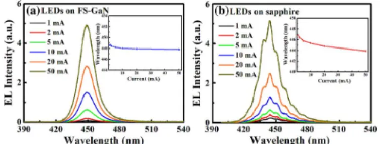
Fig. 3. EL peak wavelength at various forward current of LEDs (a) on sapphire and (b) on FS-GaN. The insert shows the spectral peak variation with the injec-tion current. (The intensities of both plots are normalized.)
regime of the LEDs on FS-GaN substrate due to lower defect density [16]. This indicates that the homoepitaxial LED has better material quality than that of sapphire [17].
Fig. 3 shows the EL spectra of the LEDs on sapphire substrate and FS-GaN substrate centered at 445 nm and 448 nm, respec-tively. The EL measurements were performed at RT with dif-ferent forward injection current in continuous wave (CW) mode. As the injection current increases from 1 to 50 mA, the peak wavelength of the LEDs on sapphire substrate shifts from 446.8 to 443.8 nm blue-shifted for 3 nm [see Fig. 3(a)]. On the other hand, the LED on FS-GaN substrate exhibits smaller blue-shift of 0.8 nm [see Fig. 3(b)]. Thus the larger blue-shift of LEDs on sapphire substrate indicates that the original quantum-con-fined Stark effect (QCSE) is much stronger than that of LEDs on FS-GaN substrate. And this phenomenon can also confirm that the strain in LEDs on FS-GaN substrate is smaller than that in LEDs on sapphire substrate [9], [17], which agrees well with our – data, further proving that homoepitaxial is an effective measure to reduce the strain in the well layers of MQW. The oscillations in EL spectra of LEDs on sapphire in Fig. 3(b) can be attributed to interference pattern due to multiple reflections within the nitride epilayers/sapphire system.
The RT optical output power of the LEDs on sapphire sub-strate and FS-GaN subsub-strate as a function of the forward in-jection current is shown in Fig. 4 insert plot. At 20 mA, the light output power of the LEDs on FS-GaN substrate is 16% higher than the LEDs on sapphire substrate. At the forward in-jection current of 300 mA, a 40% increase in the light-output power is achieved by the LEDs on FS-GaN substrate. This better
800 IEEE PHOTONICS TECHNOLOGY LETTERS, VOL. 23, NO. 12, JUNE 15, 2011
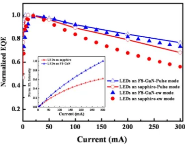
Fig. 4. Normalized external quantum efficiency as a function of forward cur-rent for LEDs on sapphire and FS-GaN under CW and pulse operations. The inserted plot is the output power versus current under CW mode.
light-output power efficiency can be particularly pronounced on FS-GaN substrate due to much larger thermal conductivity of GaN (1.3 W/cm C) than sapphire (0.258 W/cm C). The re-sults can also confirm that high quality materials, as yielded by homoepitaxy.
Fig. 4 shows the normalized external quantum efficiency (EQE) as a function of forward current for LEDs on FS-GaN and on sapphire substrates. The normalized EQE of these two types of LEDs are under continuous wave (CW) and pulse operations. The pulsed current is injected with pulse duration 2 s and duty cycle 0.1%. The difference between CW and pulsed EQE of FS-GaN sample is very small: at 300 mA, a reduction of 73% (CW) versus 76% (pulse). However, the EQE of sapphire sample shows greater difference between CW and pulsed result: 56% (CW) versus 68% (pulse).
From the reduction of dislocation, and also the improved thermal conduction of substrate, the enhancement of LED efficiency can be expected. In Fig. 4, between CW and pulsed EQE, the difference is only a few percents, while the sap-phire samples show greater differences (about 12%) between different methods. Comparing these measurements, we can quantify (in first order) that the total enhancement between pulsed FS-GaN and CW sapphire-GaN, which is 20% (76% versus 56%), can be attributed to 12% of thermal conduction improvement and 8% of material quality improvement.
IV. CONCLUSION
In summary, we have demonstrated that growing InGaN/GaN MQW on FS-GaN can improve electrical and optical properties of LEDs. As a consequence, the In GaN/GaN MQW LEDs on FS-GaN show a smaller forward voltage and ideal factor com-pared with LEDs on sapphire substrate. The blue-shift of EL peak wavelength was decreased from 3 to 0.8 nm, the injec-tion current from 1 to 50 mA. The LEDs on FS-GaN shows
about 40% increase in the light-output power compared with the LEDs on sapphire at 300 mA due to better heat dissipation. The EQE of LEDs grown on FS-GaN improved greatly in the output power, and showed much less droop at high currents. Thus use of FS-GaN substrates is a promising approach for fabrication of high power InGaN-based LEDs.
REFERENCES
[1] M. H. Kim, M. F. Schubert, Q. Dai, J. K. Kim, E. F. Schubert, J. Piprek, and Y. Park, “Origin of efficiency droop in GaN-based light-emitting diodes,” Appl. Phys. Lett., vol. 91, pp. 183507–183507-3, 2007. [2] S. Chichubu, T. Azuhata, T. Sota, and S. Nakamura, “Luminescences
from localized states in InGaN epilayers,” Appl. Phys. Lett., vol. 70, pp. 2822–2824, 1997.
[3] S. F. Chichibu, T. Azuhata, M. Sugiyama, T. Kitamura, Y. Ishida, H. Okumura, H. Nakanishi, T. Sota, and T. Mukai, “Optical and struc-tural studies in InGaN quantum well structure laser diodes,” J. Vac.
Sci. Technol., vol. B 19, pp. 2177–2183, 2001.
[4] Y. C. Shen, G. O. Mueller, S. Watanabe, N. F. Gardner, A. Munkholm, and M. R. Krames, “Auger recombination in InGaN measured by photoluminescence,” Appl. Phys. Lett., vol. 91, pp. 141101–141101-3, 2007.
[5] X. Ni, J. Lee, S. Liu, V. Avrutin, Ü. Özgür, H. Morkoç, and A. Mat-ulionis, “Hot electron effects on efficiency degradation in InGaN light emitting diodes and designs to mitigate them,” J. Appl. Phys., vol. 108, pp. 033112–033112-13, 2010.
[6] Q. Dai, Q. Shan, J. Wang, S. Chhajed, J. Cho, E. F. Schubert, M. H. Crawford, D. D. Koleske, M.-H. Kim, and Y. Park, “Carrier recombi-nation mechanisms and efficiency droop in GaInN/GaN light-emitting diodes,” Appl. Phys. Lett., vol. 97, pp. 133507–133507-3, 2010. [7] J. H. Son and J. L. Lee, “Strain engineering for the solution of efficiency
droop in InGaN/GaN light-emitting diodes,” Opt. Express, vol. 18, pp. 5466–5471, 2010.
[8] Y.-K. Kuo, J.-Y. Chang, M.-C. Tsai, and S.-H. Yen, “Advantages of blue InGaN multiple-quantum well light-emitting diodes with InGaN barriers,” Appl. Phys. Lett., vol. 95, pp. 011116–011116-3, 2009. [9] K. Akita, T. Kyono, Y. Yoshizumi, H. Kitabayashi, and K. Katayama,
“Improvements of external quantum efficiency of InGaN-based blue light-emitting diodes at high current density using GaN substrates,” J.
Appl. Phys., vol. 101, pp. 033104–033104-5, 2007.
[10] M. K. Kelly, R. P. Vaudo, V. M. Phanse, L. Görgens, O. Ambacher, and M. Stutzmann, “Large free-standing GaN substrates by hydride vapor phase epitaxy and laser-induced liftoff,” Jpn. J. Appl. Phys., vol. 38, pp. L217–L219, 1999.
[11] J. Jasinski, W. Swider, Z. Liliental-Weber, P. Visconti, K. M. Jones, M. A. Reshchikov, F. Yun, H. Morkoç, S. S. Park, and K. Y. Lee, “Char-acterization of free-standing hydride vapor phase epitaxy GaN,” Appl.
Phys. Lett., vol. 78, pp. 2297–2299, 2001.
[12] C. L. Chao, C. H. Chiu, Y. J. Lee, H. C. Kuo, P.-C. Liu, J. D. Tsay, and S. J. Cheng, “Freestanding high quality GaN substrate by associ-ated GaN nanorods self-separassoci-ated hydride vapor-phase epitaxy,” Appl.
Phys. Lett., vol. 95, pp. 051905–051905-3, 2009.
[13] C. R. Miskys, M. K. Kelly, O. Ambacher, G. Martínez-Criado, and M. Stutzmann, “GaN homoepitaxy by metalorganic chemical-vapor depo-sition on free-standing GaN substrates,” Appl. Phys. Lett., vol. 77, pp. 1858–1860, 2000.
[14] S. Chichibu, K. Wada, and S. Nakamura, “Spatially resolved cathodo-luminescence spectra of InGaN quantum wells,” Appl. Phys. Lett., vol. 71, pp. 2346–2348, 1997.
[15] E. F. Schubert, Light-Emitting Diodes, 2nd ed. Cambridge, U.K.: Cambridge Univ. Press, 2006, ch. 4.
[16] J. Xu, M. F. Schubert, A. N. Noemaun, D. Zhu, J. K. Kim, E. F. Schubert, M. H. Kim, H. J. Chung, S. Yoon, C. Sone, and Y. Park, “Reduction in efficiency droop, forward voltage, ideality factor, and wavelength shift in polarization-matched GaInN/GaInN multi-quantum-well light-emitting diodes,” Appl. Phys. Lett., vol. 94, pp. 011113–011113-3, 2009.
[17] D. Zhu, J. Xu, A. N. Noemaun, J. K. Kim, E. F. Schubert, M. H. Craw-ford, and D. D. Koleske, “The origin of the high diode-ideality fac-tors in GaInN/GaN multiple quantum well light-emitting diodes,” Appl.