Thermal stability study of Ni/Ta n-GaN Schottky contacts
G. L. Chen, F. C. Chang, K. C. Shen, J. Ou, W. H. Chen, M. C. Lee, W. K. Chen, M. J. Jou, and C. N. Huang
Citation: Applied Physics Letters 80, 595 (2002); doi: 10.1063/1.1425455
View online: http://dx.doi.org/10.1063/1.1425455
View Table of Contents: http://scitation.aip.org/content/aip/journal/apl/80/4?ver=pdfcov Published by the AIP Publishing
Articles you may be interested in
Temperature dependence of 1/f noise in Ni/n-GaN Schottky barrier diode J. Appl. Phys. 112, 024507 (2012); 10.1063/1.4737258
Electrical, microstructural, and thermal stability characteristics of Ta/Ti/Ni/Au contacts to n- GaN J. Appl. Phys. 95, 1516 (2004); 10.1063/1.1633660
Nitrogen-vacancy-related defects and Fermi level pinning in n-GaN Schottky diodes J. Appl. Phys. 94, 1819 (2003); 10.1063/1.1591417
Environmental and thermal aging of Au/Ni/p-GaN ohmic contacts annealed in air J. Appl. Phys. 91, 3711 (2002); 10.1063/1.1448885
Ni and Ni silicide Schottky contacts on n -GaN J. Appl. Phys. 84, 881 (1998); 10.1063/1.368151
This article is copyrighted as indicated in the article. Reuse of AIP content is subject to the terms at: http://scitation.aip.org/termsconditions. Downloaded to IP: 140.113.38.11 On: Thu, 01 May 2014 06:27:41
Thermal stability study of Ni
Õ
Ta
n
-GaN Schottky contacts
G. L. Chen, F. C. Chang, K. C. Shen, J. Ou, W. H. Chen,a) M. C. Lee, and W. K. Chen
Department of Electrophysics, National Chiao Tung University, Hsinchu, Taiwan 300, Republic of China
M. J. Jou and C. N. Huang
Epistar Corporation, Hsinchu, Taiwan 300, Republic of China
共Received 24 July 2001; accepted for publication 15 October 2001兲
The Schottky behavior of Ni/Ta and Ni contacts on n-GaN was investigated under various annealing conditions by current–voltage measurements. It is found that with the addition of Ta between the Ni layer and the GaN substrate the thermal stability properties of devices can be significantly improved. Experimental results indicate that a high quality Ni/Ta n-GaN Schottky diode with an ideality factor and barrier height of 1.16 and 1.24 eV, respectively, can be obtained under 1 h annealing, at 700 °C. © 2002 American Institute of Physics. 关DOI: 10.1063/1.1425455兴
Due to the properties of wide band gap, high electron saturation velocity, large breakdown field and thermal stabil-ity GaN materials have recently attracted much attention in the area of high-temperature, high-power device applications,1–3 such as metal–semiconductor field effect transistors and high electron mobility transistors. However, the realization of these devices not only counts on the quality of the material properties, but also relies critically on the performance of metal contacts, in particular the Schottky contacts. Therefore, the exploration of thermally stable Schottky contacts is very desirable for implementation of such kinds of devices. With regard to a GaN Schottky study, numbers of elemental metals, including Pd, Pt, Ti, Ni, Au, Cr and Re,4 – 8 and intermetallics of PtSi and NiSi have been investigated extensively and several advancements have been achieved.8 –9 Here, we present an alternative method that uses a Ni/Ta contact scheme to improve the thermal stability properties of the GaN Schottky contact. We ob-served that a high quality Schottky diode with an ideality factor and barrier height of 1.16 and 1.24 eV, respectively, can be obtained for samples annealed under severe annealing conditions of 700 °C for 1 h.
The 2-m-thick n-GaN film employed here was pre-pared using metalorganic vapor phase epitaxy. The corre-sponding background concentration and electron mobility are 1.7⫻ 1017cm⫺3 and 566 cm2/V•s, respectively. In or-der to characterize electrical properties, Ni/Ta Schottky di-odes were then made for these samples.
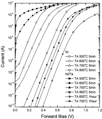
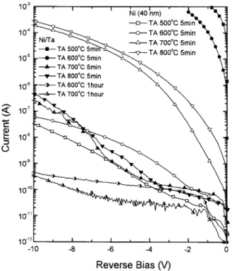
In Figs. 1 and 2, we present the dependence of the for-ward and reverse bias characteristics of pure Ni and Ni/Ta bilayer Schottky contacts on n-GaN annealed at various tem-peratures from 500 to 800 °C from 5 min to 1 h, respectively. From the forward log I – V curves, the ideality factors n, Schottky barrier heights b, and saturation current Is of these diodes can be obtained. The extracted device param-eters for these Schottky diodes are summarized in Table I.
As far as the Ni/n-GaN Schottky diodes are concerned, under a fixed annealing time of 5 min we find that the for-ward I – V curve共open symbols兲 tends to shift to the left 共low
voltage and high current兲 with an increase in temperature, indicating poorer rectifying characteristics have occurred in these high-temperature annealed Ni diodes. Clearer pictures can be seen from the deduced device parameters. As can be seen in Table I, despite the fact that a good quality Schottky diode with an ideality factor of 1.14 and barrier height of 0.93 eV can be obtained at an annealing temperature of 500 °C, a further increase in the annealing temperature does deteriorate the I – V characteristics, particularly that of the barrier height. It changes to 0.85 eV at 600 °C, 0.76 eV at 700 °C, and 0.70 eV at 800 °C. Such degradation is attribut-able primarily to the onset of interface reactions of Ni and GaN and a burst of loss of N at the interface at 550– 600 °C,
a兲Electronic mail: [email protected]
FIG. 1. Forward I – V characteristics of Ni and Ni/Ta n-GaN Schottky con-tacts after being annealed at temperatures from 500 to 800 °C for 5 min or 1 h, respectively.
APPLIED PHYSICS LETTERS VOLUME 80, NUMBER 4 28 JANUARY 2002
595
0003-6951/2002/80(4)/595/3/$19.00 © 2002 American Institute of Physics
This article is copyrighted as indicated in the article. Reuse of AIP content is subject to the terms at: http://scitation.aip.org/termsconditions. Downloaded to IP: 140.113.38.11 On: Thu, 01 May 2014 06:27:41
in accord with the arguments given by Liu et al.,9by Bermu-dez and Kaplan,10and by Venugopalan et al.11
In contrast, very unlike behavior is observed in the Ni/Ta
n-GaN Schottky diodes after annealing at various high
tem-peratures for 5 min. As can be seen in Fig. 1, when Ta is added to the contact layer the corresponding forward I – V curve 共closed symbols兲 tends to shift to the right with an increase in annealing temperature, rather than the tendency to shift to the left in the Ni-only diodes. Moreover, it is worth mentioning that the Ni/Ta Schottky diode displays virtually no rectifying characteristics at annealing temperatures of 500– 600 °C. It improves almost immediately after the tem-perature exceeds 700 °C. The resultant ideality factor n is almost close to 1 and the barrier heights are 1.12 and 1.16 eV, respectively, for 700 and 800 °C samples. Such good Schottky characteristics are unusual for high-temperature an-nealed GaN diodes.
To examine the long-term thermal stability of the Ni/Ta GaN Schottky diode, we conducted further experiments with
an extended annealing time of 1 h at 600 and 700 °C, respec-tively, and of 30 min at 800 °C. The results are also shown in Figs. 1 and 2 and in Table II. It is interesting to note that no clear evidence of degradation is observed for 600 and 700 °C annealed diodes under prolonged thermal treatment. In fact, slightly better results are obtained for these diodes. The cor-responding ideality factor remains almost unchanged, but the barrier height improves from 1.12 to 1.17 eV for 600 °C and 1.16 –1.24 eV for 700 °C as the annealing time is increased from 5 min to 1 h. As for the 800 °C sample, insulator-like behavior is observed for an annealing time of 30 min.
For thermal stability study of GaN, it has been demon-strated that both conventional Pt and N GaN Schottky diodes,8,9can be stable up to 400–500 °C for 1 h annealing, as shown in Table II. The addition of Si to the Pt GaN diode is found to have a noticeable effect in improving the thermal stability compared to the Pt-only diode, for which the an-nealing temperature can be increased up to 600 °C for 1 h without severe degradation of its performance. Although Venugopalan and Mohney6in their study have shown that a Re contact is more thermal stable than most reported GaN Schottky contacts, satisfactory rectifying characteristics can only be obtained at an operating temperature as high as 150 °C. Based on the above discussions, we determine that our Ni/Ta/n-GaN does perform comparatively well with re-gard to the thermal stability since a high quality Schottky diode with a barrier height of 1.24 eV and an ideality factor of 1.16 can still be obtained at a temperature of 700 °C for less then 1 h annealing.
One additional point worth mentioning is that when the Ni/Ta GaN Schottky diode is subjected to long-term expo-sure, for example, 1 h, at 600 or 700 °C, the reverse leakage current is reduced to a value of 10⫺7A/cm2 and exhibits nearly voltage-independent characteristics. These findings to-gether with the excellent forward characteristics seem to im-ply that the metal–semiconductor interface that results in this case is highly metallurgically stable and nearly free of any interface reactions and component interdiffusion共which will be discussed in more detail later兲 since, if imperfections do occur, they will form an intervening dipole layer and other contaminants at the interface and cause an increase in leak-age current at high reverse bias voltleak-age.
The strong dependence of electrical properties in the Ni/Ta/n-GaN Schottky diode on the annealing temperature FIG. 2. Reverse I – V characteristics of Ni and Ni/Ta n-GaN Schottky
con-tacts after being annealed at temperatures from 500 to 800 °C for 5 min or 1 h, respectively.
TABLE I. Electrical parameters of Ni/ and Ni/Ta/n-GaN diodes.
Metal Annealing temperature 共°C兲 Ideality factor n Barrier height,b 共eV兲 Series resistance, Rs 共⍀兲 Leakage current, JR 共A/cm2兲 Ni 500, 5 min 1.14 0.93 200 1⫻10⫺6 600, 5 min 1.20 0.85 250 1⫻10⫺5 700, 5 min 1.21 0.76 250 1⫻10⫺2 800, 5 min 1.21 0.70 280 2.5⫻10⫺2
Ni/Ta 500, 5 min Poorly rectified
600, 5 min Poorly rectified
700, 5 min 1.08 1.12 600 1.5⫻10⫺6
800, 5 min 1.08 1.16 950 1.5⫻10⫺6
600, 1 h 1.09 1.17 650 9.5⫻10⫺7
700, 1 h 1.09 1.24 3800 1⫻10⫺7
800, 30 min Insulator like
596 Appl. Phys. Lett., Vol. 80, No. 4, 28 January 2002 Chenet al.
This article is copyrighted as indicated in the article. Reuse of AIP content is subject to the terms at: http://scitation.aip.org/termsconditions. Downloaded to IP: 140.113.38.11 On: Thu, 01 May 2014 06:27:41
and annealing time is believed to correlate closely to the degree of partial oxidation of the Ta metal layer, as con-firmed by our Auger electron spectroscopy depth profile analysis and x-ray photoelectron spectroscopy measurements published in a previous paper.12 The presence of oxygen in all of our samples except the as-deposited one clearly indi-cates that the oxygen originates primarily from the process environment during the thermal annealing step. For the ex-perimental setup used here, we have found that the Ta film starts to oxidize at 400 °C and almost fully converts into tantalum oxide at 700 °C and above, particularly for long-term exposure. Thus, the evolution of electrical properties for the Ni/Ta/n-GaN diode on the annealing temperature can be inferred as follows. When the sample is annealed at low temperatures where the amount of unintentionally oxygen introduced into the contact region is still rather small, the Ta near the GaN remains in its elemental form. The resulting Ni/Ta/n-GaN film in this case behaves virtually the same with respect to the forward and reverse I – V characteristics, i.e., nearly ohmic characteristics, as the Ta/n-GaN diode. On the other hand, when the oxidation of Ta is more complete, the Ni/Ta/n-GaN diode becomes more of a metal–insulator– semiconductor type structure and the effective barrier height in this case is determined largely by the physical parameters of the Ni and Ta2O5layers and the GaN substrate, including
the work function, electron affinity and Schottky barrier pin-ning factor S. By employing S⫽0.4,13 the calculated barrier height for pure Ni on Ta2O5is⬃1.4 eV, very close to that of
the observed maximum barrier height, 1.24 eV, in our Ni/Ta/n-GaN diodes. But if the diode is subjected to pro-longed exposure at a higher temperature the tantalum oxide becomes too thick for the carriers to flow over and as a result insulator-like diode behavior is observed for our 800 °C GaN diode.
With regard to the thermal stability of these diodes, it is known that tantalum oxide possesses a relatively low Gibbs formation energy, G(Ta2O5)⫽⫺484 Kcal/mol, compared to
G(Ga2O3)⫽⫺260, G(Ta2N)⫽⫺65 and G(GaN)
⫽⫺26.4 Kcal/mol,14 and once the tantalum oxide has
formed, the oxide–semiconductor interface becomes quite thermodynamically stable. It not only successfully stops the outdiffusion of Ga and N from the substrate, but also essen-tially prevents the penetration of Ni into GaN and
accumu-lation on its surface to form metal gallides that will degrade the Schottky performance. Thus, the formation of a highly stable thin tantalum oxide layer between Ni and the GaN substrate may be the reason for the good thermal stability of our Ni/Ta/n-GaN diodes.
In summary, we have carried out an electrical study of a Ni/Ta/n-GaN Schottky diode under prolonged exposure at high temperatures. Our results indicate better Schottky per-formance can be obtained for an n-type GaN diode if an intermediate Ta layer is added between Ni and the GaN sub-strate. After high temperature annealing, the optimum ideal-ity factor and barrier height can reach values of 1.08 and 1.24 eV, respectively. More important, it is found that high quality diode performance can still be obtained for these di-odes under 700 °C, 1 h thermal annealing, which is unusual for an n-GaN Schottky diode. The above finding suggests a Ni/Ta Schottky contact is potentially useful for GaN high-temperature, high-power device applications.
The authors would like to acknowledge financial support from the National Science Council, Republic of China, under Contract Nos. NSC89-2212-M009-061 and -056.
1Z. Fan, S. N. Mohammad, O. Aktas, A. E. Botchkarev, A. Salvador, and H.
Morkoc, Appl. Phys. Lett. 69, 1229共1996兲.
2Q. Chen, M. Asif Khan, J. W. Yang, C. J. Sun, M. S. Shur, and H. Park,
Appl. Phys. Lett. 69, 794共1996兲.
3
J. C. Zolper, R. J. Shul, A. G. Baca, R. G. Wilson, S. J. Pearton, and R. A. Stall, Appl. Phys. Lett. 68, 2273共1996兲.
4A. C. Schmitz, A. T. Ping, M. A. Khan, Q. Chen, J. W. Yang, and I.
Adesida, Semicond. Sci. Technol. 11, 1464共1996兲.
5
A. T. Ping, A. C. Schmitz, M. A. Khan, and I. Adesida, Electron. Lett. 32, 68共1996兲.
6H. S. Venugopalan and S. E. Mohney, Appl. Phys. Lett. 73, 1242共1998兲. 7J. D. Guo, M. S. Feng, R. J. Guo, F. M. Pan, and C. Y. Chang, Appl. Phys.
Lett. 67, 2657共1995兲.
8
Q. Z. Liu, L. S. Yu, S. S. Lau, J. M. Redwing, N. R. Perkins, and T. F. Kuech, Appl. Phys. Lett. 70, 1275共1997兲.
9Q. Z. Liu, L. S. Yu, S. S. Lau, F. Deng, and J. M. Redwing, J. Appl. Phys.
84, 881共1998兲.
10
V. M. Bermudez and R. Kaplan, Phys. Rev. B 48, 2436共1993兲.
11
H. S. Venugopalan, S. E. Mohney, B. P. Luther, S. D. Wolter, and J. M. Redwing, J. Appl. Phys. 82, 650共1997兲.
12G. L. Chen, F. C. Chang, W. C. Chuang, B. R. Huang, W. C. Chen, M. C.
Lee, and W. K. Chen, Jpn. J. Appl. Phys., Part 2 40, L255共2001兲.
13
J. Robertson and C. W. Chen, Appl. Phys. Lett. 74, 1168共1999兲.
14D. R. Lide, Handbook of Chemistry and Physics, 72nd ed. 共Chemical
Rubber, Boston, 1991–1992兲. TABLE II. Comparison of Schottky properties of GaN diodes.
Metal Ideality factor, n Barrier height,b (I – V) 共eV兲 Barrier height,b (C – V) 共eV兲 Stable temperature 共°C兲 Reference Ni共100 nm兲 1.16 ¯ 1.06 400, 5 min 7 Ni共100 nm兲 1.10 0.88 1.09 500, 1 h 9 Pt 1.16 0.73 0.91 400, 1 h 8 Pd共200 nm兲 1.04 0.94 1.07 300/5 min 4 Re共70 nm兲 1.09a 0.78 1.03 700/10 min 6 Ni/Ga/Ni ¯ ¯ ¯ 700/10 min 11 NiSi共Ni/Si/Ni兲 1.14 0.86 1.47 600/1 h 9 PtSi共Pt/Si/Ni兲 1.12 0.69 0.74 600/1 h 8
Ni/Ta共50/50 nm兲 1.09 1.17 ¯ 700/1 h This work
a
Operation temperature of 150 °C.
597
Appl. Phys. Lett., Vol. 80, No. 4, 28 January 2002 Chenet al.
This article is copyrighted as indicated in the article. Reuse of AIP content is subject to the terms at: http://scitation.aip.org/termsconditions. Downloaded to IP: 140.113.38.11 On: Thu, 01 May 2014 06:27:41