2004 IEEE Asia-Pacific
Conference on Advanced System Integrated Circuits(AP-ASIC2004)I Aug. 4-5,2004
11-7
A Hardware Efficient
64-QAM Low-IF Transceiver Baseband
for
Broadband Communications
Ching-Chi
Chang, Muh-Tian Shiue*, and Chomg-Kuang Wang Graduate Institute of Electronics Engineering, and Department of Electrical Engineering,National Taiwan University, 106 Taipei, Taiwan R.O.C.
*Department of Electrical Engineering, National Central University, 320 Jung-Li, Taiwan R.0.C E-mail: [email protected]
AbslmcI-This paper presents a hardware efficient VLSl design of digital baseband for 64-QAM communication systems over the last- mile cable network. This VLSI system design involves a mt-efficient architecNre of the adaptive equalizer and a two-phase linear architecture of the pulse shaping filters, which d u c e the hardware requirement by a factor of four comparing with traditional quadrsture d i m t form FIR filters. In this design, the two.fold carrier recovery Imp possesses
a pull-in range of i l O O k H z (i.e. f18,500ppm of the symbol rate) and -82dBc jitter suppr?ssion. Based on the proposed multi-staged LMS-based fractionally-spaced equalizer, the receiver realizer the symbol spaced timing recovery in a i200ppn tolerance of the symbol rate. The acquisition time of the proposed 64-QAM blind adaptive system is 7ms, and the transceiver reaches the operation speed of the case for
32.28Mbls 64-QAM low-IF digital CATV system over NTSC 6MHz
bandwidth channels. Using 0.35pm CMOS technology, the transceiver design occupies a chip area 5.5mm x 5.5mm and power consumption 1.35W (1.OW for RX) when the power supply is 3.3V.
1. INTRODUCTION
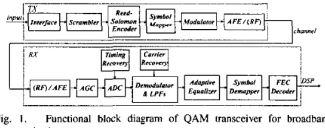
Fig.1 shows a typical functional block diagram of QAM transceiver for last-mile broadband digital communication systems, such as digital CATV [I], SCM-VDSL [2] and Wireless MAN [3]. The transmitter mainly consists of an FEC encoder, a symbol mapper, a Nyquist pulse shaping filter (PSF), a quadrature mixer, and the analog front end (AFE). In the receiver, a digital quadrature mixer and two identical low-pass filters (LPFs) are used to demodulate the received passband signal. The coherent carrier recovery (CR) loop is employed to combat the performance degradation from non-coherent receiving. The timing recovery (TR) loop for symbol timing synchronization provides the ADC a proper sampling instant. In order to combat the IS1 caused by the band-limited channel, an adaptive equalizer with blind adaptation is utilized.
In a conventional architecture of a baseband adaptive QAM decision feedback equalizer (DFE), both feed forward (FF) and feedback (FB) filters contain tens to hundreds adaptive complex laps. This requires a significant hardware on an S K chip. In order to
reduce the chip area, the equalizer can employ a multiplication- and-accumulation (MAC) unit with higher clocking rate by paying the power consumption and circuit complexity [4]. Practically, this advantage will be eliminated when the equalizer is designed to combat various channel conditions with variable equalization tap numbers [1][5]. In a coherent receiving, it i s then imperative to extract frequency and phase of the canier from the incoming signal 161. Most of the data modems require fast carrier frequencylphase acquisition in the starlup and high jitter suppression in the steady state. In practice, it is hard to he satisfied in a simple CR loop, especially when the RF local oscillator (LO) frequency offset has to be taken into account in RF transmission systems [ 1][3]. In order to reduce the transceiver chip area, the PSF in the transmitter and the LPF in the receiver can be replaced by image rejection lowpass filters (IRLFs) 171. The IRLF is a linear-phase half-hand filter with an YQ-path interleaving
scheme. The hardware cost of the IRLF can be further reduced by eliminating the long delay line which is proportional to the number of coefficient taps.
Fig. I. Funaianal block d i a p m of QAM tr~nsceiver for broadband communications
Based on the QAM transceiver architecture shown in Fig.1, this paper presents a hardware efficient architecture for thc multi-stagc LMS-based blind equalizer. The proposed pipeline architecture of the equalizer shown in Fig.3 processes some parallel parts sequentially to reduce the hardware requirement by a factor of four comparing with the architecture implemented directly from the transfer function. Taking the advantage of the TI2 fractionally spaced equalizer, the TR loop shown in Fig.4 utilizes a haud-rate decision-directed early-late timing extraction scheme to achieve a &200ppm timing frequency
tolerance within 7m,s acquisition. Since it is mandatoty to provide wide locking range and low jiner variation of carrier recovery in a high constellation Qkn RF uansmission system, the proposed two-fold CR loop can achieve a locking range ilO0kHz (i.e. il8,500ppm of the symbol rate) and jitter suppression -82dBc for
carrier retrieval in a single architecture as shown i n Fig.7. In order to further reduce the hardware complexity, the proposed architecture shown in F i g 2 for the two-phase linear FIR filter can actualize higher hardware efficiency than an IRLF can do.
The organization of this paper is as follows. The transceiver design is presented in Section 11. Section 111 presents VLSI implementation considerations of the transceiver. Section IV shows the simulation results. and the conclusion will he drawn in section V.
11. TRANSCEIVER ARCHITECTURE
In this hansceiver VLSI architecture design, the 64-QAM 4 . 0 3 5 MH z low-IF digital CATV system is demonstrated. Based on the various digital CATV channel models [SI, all the functional blocks are designed to overcome the non-ideal transmission circumstances.
A. Transmitter
In the proposed QAM transmission system, in order to avoid the drawback of analog demodulation, such as DC offset and mismatch between quadrature paths, the low-IF 4.036MHz modulator is implemented in digital domain. In addition, the anti-sinc FIR filter
2004 IEEE Asia-Pacific Conference on Advanced System Integrated Circuits(AP-ASIC2004)/
Aug.
44,2004
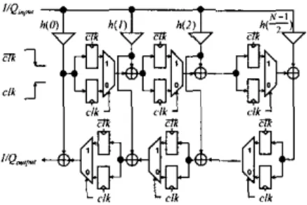
with linear phase is used to compensate the inherent DAC distortion. The square-root raised-cosine filters with a roll-off factor 0.1152 are employed for both transmitter PSFs and receiver LPFs in the CATV system. The proposed two-phase linear FIR filter architecture shown in Fig.2 translates the linear phase FIR filter into a linear phase halfband filter. Using the two-phase clocking technique, the in- phase data are latched by the negative clock edge in upper registers while the quadrature data are latched by the positive clock edge in the lower registers. The mutiplexers (MUXs) are controlled by the clock phase to pass the in-phase data to the adders when the clock is high. In contrast, the quadrature data is passed to the adders when the clock is low. Comparing with the traditional quadrature direct form FIR filter, which is composed of 2N multipliers and (2N - 2) adders, the hardware complexity is reduced to
(N+
1)/2 multipliers and ( N - 1) adders. where N is the tap number of the quadrature PSF. The power consumption is approximately half of the traditional quadrature direct form FlR filter.easily set up according to the channel condition by the hand-shaking protocol during the startup of the transmission.
clW4
Fig. 3. equalizer
T h e proposed 8-stage pipeline architecture far the adaptive blind
j
-1
DAC H.-.mterW Phase... I
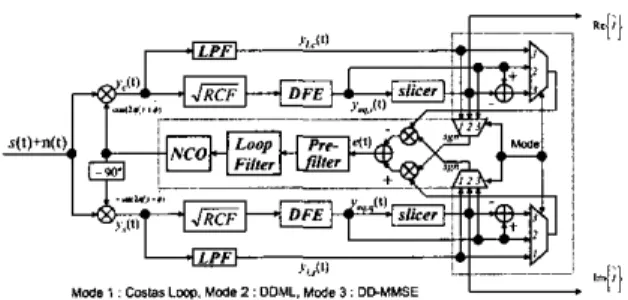
Fig. 4. R e receiver archilecture using mixed-made baud-rate liming rewvery
loop
Fig. 2. Thc proposed two-phase architecture for the pulse shaping filter
B. Adaptive Equalizer
modified LMS algorithm is shown in the following.
Based on the multi-stage and signed delay-LMS algorithm
[a],
theC(n
+
1) = C(n)+
p.
r(n - 1).
sgn(e*(n-
1)) (1) where C(n) is the adaptive complex coefficient. p i s the updating step size, which is designed to be a number of power of two for scaling the signal r ( n-
1).
sgn(e'(n - 1)) in each adaptive stage with a factor of two to eliminate multiplications. e(n) and r(n) are the error message and the received signal, respectively, and the complex multiplier is replaced by a two's complementer. A stop-and-go flag mechanism [9] associated with IL is introduced for blind updating. The reduced constellation algorithm (RCA) is adopted to blindly start the equalizer in the acquisition state.1f the direct form and fully parallel process are employed to construct complex filter banks, it will consume (4N
+
4M) real multipliers and adders, where N and M are FF and FL3 tap numbers respectively. In order to reduce the hardware cost and circuit complex- ity at the same time, the 8-stage pipeline architecture shown in Fig.3 is proposed. The clk in Fig.3 is %times of symbol clock rate, i.e. 43.04MHe. The complex-value convolution is sequentially performed by four real value convolutions during the preliminary three hardware stages. After decreasing delays, the real value convolution results are ready at T3 to 7'6, and complex-value sums, slicing, equalized signal SNR calculations and 118 decimation are performed in the final stages, T6 and T7. The proposed pipeline architecture of the blind adaptive equalizer consumes ( N+
M ) real multipliers and adders which is only a quaner of the architecture implemented directly from the transfer function. The programmable numbers N and M can be"
...
IFig. 5. The phase detector and lhe loop filter of the timing recovery loop
C. Timing Recovery
Instead of suffering signal SNR degradation in an all-digital TR I m p with an interpolator, the mixed-mode TR loop architecture shown in FigA is devised. Practically. the stochastic estimation tech- nique cooperated with a digital phace-locked-loop (PLL) is employed to maintain system stability. Based on the baud-rate early-late timing estimation algorithm shown in Eq.(2) [IO], the decisiondirected early-late timing estimation derived in E.4.(3) is proposed.
e ( i ) = %An
.
[yeq(T, i)-
yeq(-T, 7)1> (2) e(.) = Elsgn(in(7)) ' [?/eq,n+t(i) - Yeq,n-l(T)]} (3) where A, and yeq are transmitted and equalized signals, respectively, and I , is the decision result. The digital multiplier can be avoided by using the sign bit of the slicer output. Fig.5 shows the circuit of the phase detector and the loop filter of the baud-rate TR loop. Preceded the proportional and integral (PI) loop filter, an 11R pre- filter is employed to suppress the noise power. This pre-filter is of 5 to 10 times wider bandwidth than the I m p filter, and the closed loop architecture can be treated as a second order PLL.2004
IEEE
Asia-PacificConference on
AdvancedSystem
Integrated
Circuits(AP-ASIC2004)/ Aug.4-5,2004
D. Carrier Recovery
Clhe proposed CR loop has three operation stages [61. In the acquisition state, the two-fold CR loop is configured to be the prior CR loop, a modified Costas loop shown in Eq.(4), and stam at time A as shown in Fig.6(a). At time B. the two-fold CR loop is switched to the posterior CR loop when the adaptive equalizer converges roughly. Meanwhile, the DC component of the prior CR loop output, wdC. is extracted and added to the initial frequency of the numerical-control-oscillator (NCO). The posterior CR loop begins with the NCO frequency at WO
+
wdc as shown in Figd(b). In this tracking state, the equalizer operates in an ISI-affected converged mode and the CR performs decision-directed maximal-likelihood (DD-ML) phase estimation derived in Eq.(5). At time C. the equalizer fully converges and the C R loop is further switched to a decision- directed minimum-mean-square-error (DD-MMSE) phase estimation shown in Eq.(6). Using the equalized signal, the CR loop provides high jitter suppression in the steady state. The proposed architecture shown in Fig.7 is hardware efficient since the three-staged operation and the two-fold architecture share most of the circuit functions.4 M L = -Irn{sgn(i') ' Y l ( t ) } (4) 4 M L = -Im{i* .ye&)} ( 5 )
4 , ~ s ~ = E{ [ ~ e q ( t ) -
f]'
. a g n ( y e q ( t ) ) } ( 6 )(4
( b )Fig. 6.
recovery loop (b) Posterior carrier recovery loop 161
The behavior of two-fold carrier recovery loop (a) Prior carrier
this chip for automatic verification. The head-end transmitter function is also included for system self testing. Using TSMC 0.350711 lP4M CMOS technology, the chip occupies 5.5mm x 5.5mm chip area as shown in Fig.8.
Fig. 8.
CATV Modem
The layout for 4 . 0 3 5 M H z Low-IF digilal baseband of 64-QAM
IV. SIMULATION RESULTS
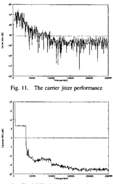
Using the post-layout extracted circuit under 4 process corners, the digital baseband transceiver is simulated in all transmission channel models. The tolerance of the carrier offset in a digital CATV system is 1100kHz. i.e. *la, 500ppm of the symbol rate, as shown in Fig.9. Fig.10 shows the frequency convergence of the TR loop when the symbol timing offset is as large as i 2 0 0 p p m . As soon as the receiver enters the steady state, the carrier jitter can be reduced down to -82dBc@100kHz away from the carrier frequency, as shown in
Fig.1 I . Fig.12 shows the mean-square-error (MSE) of the q u a i i r e d
signal. The constellation for decision in the steady state is shown in Fig.13. The acquisition time is i'rns, which is much less than the requirement of lOOms in a CATV system. Table I summarizes the simulation performance of this 64-QAM Low-IF transceiver digital baseband chip.
_i
I
1
D - . - I - -
-1-Y-
Fig. 9. The +100hH1 compensation frequency of the carrier recovery loop
Fig. 7. The proposed archilecrure lo realize the threestaged two-fold canier
recovery loop 161
I l l . VLSI IMPLEMENTATION CONSIDERATIONS Three approaches of the VLSI design are employed. The non- regular functional blocks are written in a high level description language (HDL) and synthesized using standard cell methodologies. Then, the clock trees and control signals are manually synthesized to ensure timing constraints. Finally, !he dedicated multipliers and adders are synthesized by CAD tools with specifications of delay, area, styles and power. In addition, a self-test circuit is also built in
I -1 3- I-
-
_m1 - u _ n
Fig. IO. The +2OOpprn cornpensalion frequency of the timing recovery loop
2004 IEEE Asia-Pacific Conference on Advanced System Integrated Circuits(AP-ASIC2004)/ Aug. 4-5,2004
System Clock
n/c_
Fig. I I . The carrier jitter performance
43.04MHr
T “ . r n I _
Fig. 12. The MSE of the blind adaptivc equalizer
IF Frequency PSFLPF Tsp Number Anti-sinc Filter Tap Number
Equalizer Tap Number
V. CONCLUSION
This paper presents a hardware efficient VLSI architecture of digital baseband for 64-QAM low-IF digital CATV system with data rate 32.28Mbls. Taking the advantage of the proposed multi-staged LMS based blind equalizer. timing offset tolerance HOOppm of the
baud rate TR loop and pull-in range better than 5OOppm with
-82dBc jitter suppression of the two-fold CR loop are demonstrated. Both architectures of the adaptive equalizer and the two-phase linear pulse shaping filter contribute the most hardware reduction in this
transceiver chip. Since single carrier modulation (SCM) technology is considered one of the main candidates for the Wireless MAN system [3], the proposed architecture, which contains the transmitter, synchronous loops and the programmable blind equalization, can be applied to fixed broadband wireless access networks.
REFERENCES
[ I ] Digital Audio-visual Council. “Lawer layer pmtoeols and physical interfaces,” DAVlC 1.2 Spec@cation Pan 8, Rev 4.2, 1997. [2] TIE1.4, “Vdsl technical specification. pan 2: Technical specification for
B single-carrier modulation (scm) transceiver.,” Working Gmup TIE1 (DSL Acces), Greensboro, NC. February 2WI.
4.035MHz 39
9 m 2 1 . m:19 Timing Recovery Tolerance
Carrier Recovery Tolerance Carrier JitIer Performance Equalizer SNR Performance
Receiver Acquisition Time Rocess Technology Gate Count i2ooppm i l O O k H l -8ZdBe~lOOkHr 30dB 7ms TSMC 0.35fim 1P4M 280.195 L ~~ Supply Voltage 3.3v
Power Consumption 1.35W (RX1.OW) Chip Size 5.5mm x 5.5mm
[3] IEEE Standard for Lacal and Metropolitan Area Networks. “Pan 16: Air interface for fixed broadband wireless access systems-amendment 2 Medium access control modifications and additional physical layer specifications far 2-1 1 ghz,” April 2W3.
[4] C. F. Wu. M. T. Shiue, C. C. Huang, and S. 1. IOU, “Qadvsb dual
mode equalizer design and implementation:’ AP-ASIC, pp. 323 -326. Aug 1999.
“Very-high bit-rate digital subscriber lines (vdsl) metallic interface, pan I : Functional requirements and common specification,”
Working Gmup TIE1 (DSL Access), Vancouve,: Canada. February 2002.
[61 C. C. Chang, C. C. Lin. M. T. Shiue, and C. K. Wan& “A wide pull-in
range fast acquisition hardware-sharing two-fold carrier recovery loop.”
ISCAS, vol. 4, no. 12, pp. 358-361, May 2001.
171 L. K. Tan, 1. S. Putnam. and E Lu, “A 70-mbls variable-rale IOZCqam
cable receiver ic with integrated IO-b adc and fec decoder:’ IEEE 3. Solid Stole Cirerrit, vol. 33, no. 12, pp. 2205-2218, Dec 1998. [8] M. T. Shiue, Transceiver V U 1 Design for High Speed Local Access
Moderns. Ph.D. thesis, National Cenlral Univ., Taiwan R.O.C., Scpt
1998.
[91 G. Picchi and G. Prati. “Blind equalization and carrier recovery using a
slop-and-go decesion-directed algorithm.:’ IEEE Trans. Commun., vol.
COM-35, no. 9, pp. 877487, Sepl 1987.
1101 K. H. Mueller and M. Muller, ‘Thing recovery in digital synchronous data receivers:’ IEEE Trans. Commun.. vol. COM-2.1, pp. 516-531, May 1976.
[ 5 ] TIE1.4.