ISCAS 2000
-
IEEE International Symposium on Circuits and Systems, May 28-31, 2000, Geneva, SwitzerlandA NOVEL TWO-PORT 6T CMOS S U M CELL STRUCTURE FOR
LOW-VOLTAGE VLSI SRAM WITH SINGLE-BIT-LINE SIMULTANEOUS
READ-AND-WRITE ACCESS (SBLSRWA) CAPABILITY
B. ?:
Wang
and
James
B. Kuo
Rm. 338, Dept. of Electrical Eng., National Taiwan University Roosevelt Rd., Sec.
4,
Taipei, Taiwan106-17
Fax:886-2-2363-6893,
Telephone:886-2-2363-525
1x338Email:[email protected]
Abstract
This paper reports a two-port 6T CMOS SRAM cell structure for low-voltage VLSI SRAM with single-bit-line simultaneous read-and-write access (SBLSRWA) capability. With a unique structure by connecting the source terminal of an NMOS device in the SRAM cell to the write word line, this SRAM cell can be used to provide SBLSRWA capability for 1V two-port VLSI SRAM as verified by SPICE results.
Summary
Introduction
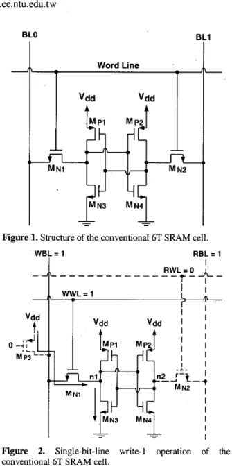
In a conventional SRAM cell as shown in Fig. 1, double bit lines have been used for read and write accesses -read and write operations are done via the same pair of bit lines. Therefore, while designing two-port memory IC with simultaneous read and write capability, two more pass- transistors and an extra pair of bit lines are needed to be incorporated into the memory cell. As a result, the size of the memory cell is increased substantially. If the memory cell structure can be simplified to provide the operation with only one bit line for read and the other bit line for write, the size of this memory cell can be reduced a lot for implementing two- port VLSI SRAM.
The difficulty of using the conventional SRAM cell with single-bit-line write access can be perceived from Fig. 2. As
shown in Fig. 2, if logic-1 is to be written from the left bit line WBL via the pass transistor MNI into the left side of the memory cell (node nl), where logic-0 is originally stored. During the write-in operation, the voltage at node n l cannot
be raised to exceed Vdd - Vm by the write bit line WBL, where v d d is the power supply voltage and Vm is the
threshold voltage of the pass transistor MN,. In addition, since the ratioed-logic structure, which is made ,of the NMOS devices MNI and MN3 in the memory cell and the PMOS device Mp3. which is the driver of the bit line WBL, plus the fact that the electron mobility of the NMOS devices
This work is supporte'd under R.O.C. National Science Council Contracts #88-22 15-E002-033 & #88-2622-E002-028.
B LO
I
Figure 1. Structure of the conventional 6T SRAM cell.
RBL = 1
'If1
- - - _ _ _ _
~ R W L l E-
W L = 1
Figure 2. Single-bit-line write-1 operation of the
conventional 6T SRAM cell.
is larger than the hole mobility of the PMOS device, the
0-7803-5482-6/99/$10.00 a2000 IEEE
voltage of node n l is difficult to be raised during the single- bit-line write-logic- 1 operation. As a result, the conventional
SRAM cell structure cannot be used for two-port memory circuits with the single-bit-line write-logic- 1 operation. Although several techniques [1]-[2] have been applied to resolve this difficulty, the penalty cannot be justified for realizing two-port VLSI SRAM. Using DTMOS techniques, a two-port 6T SO1 CMOS SRAM cell for low-voltage SRAM with SBLSRWA has been reported [3]. In this paper, with a unique structure by connecting the source terminal of an NMOS device in the S Wcell to the write word line, this 6T SRAM cell can be used to provide single-bit-line simultaneous read-and-write access capability for 1V two- port VLSI SRAM.
SBLSRWA
$RAM
Cell
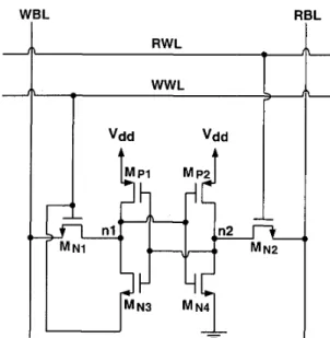
Fig. 3 shows the single-bit-line simultaneous read-and-write access (SBLSRWA) two-port 6T SRAM cell. As shown in the figure, the source terminal of the NMOS device MN3 is connected to the write word line WWL instead of to the ground as in the conventional SRAM cell. In the SBLSRWA memory cell, the left side is connected to the write bit line WBL via the pass transistor MN,, which is controlled by write word line WWL. The right side of the SBLSRWA memory cell is connected to the read bit line RE3L via the pass transistor MN,, which is controlled by the read word line
RWL. By this configuration, simultaneous read and write accesses of the SBLSRWA can be facilitated. During the write-logic-1 access, initially, logic-0 is stored at node n l . The previous problem associated with the turn-on of the
Figure 3. Structure of the two-port simultaneous read-and-
write access (SBLSRWA) 6T SRAM cell.
NMOS device M,, in the conventional SRAM cell for single-bit-line write-logic- 1 access can be avoided. Instead, owing to the write word line WWL-connected source terminal of MN3, during the single-bit-line write-logic- 1 operation, the source of the NMOS device M,,is tied to high, usually at Vdd. As a result, during the single-bit-line write- logic-1 operation, the voltage of node n l can reach high at Vdd - Vm easily. Consequently, MN4 turns on and Mp2 turns off. Thus, the right side of the SBLSRWA cell, node n2, switches to OV, which makes the voltage of node n l raised to 1V. This concludes the write-logic- 1 operation.
In order to verify the effectiveness of the SBLSRWA SRAM
cell, transient analysis during simultaneous read and write accesses of the SBLSRWA SRAM cell at a low supply voltage has been carried out. In the SBLSRWA SRAM cell under study, all six transistors have an aspect ratio of 0.3pd0.25pm. Two parasitic capacitors of O.1pF are assumed at write and read bit lines (WBL, RBL). Based on a 0.25pm CMOS technology, Fig. 4 shows the transient waveforms during the write access of the SBLSRWA 6T
SRAM cell at
v&,
of 1V based on SPICE simulation results. As shown in the figure, there are four cases for the write access-
(1) logic-0 is written into the storage node n l , which is stored with logic-0 (logic-0 + logic-0), (2) logic-1 is written into the storage node n l , which is stored with logic-0 (logic-0+
logic-1), (3) logic-1 is written into the storage node n l , which is stored with logic-1 (logic-1+
logic-1), (4)logic-0 is written into the storage node n l , which is stored with logic-1 (logic-1+
logic-0). The transients associated with these four cases are described below.I
cp"
0.4 0.21
I I I -0 I 5 10 ' - 1 1- 20 25 Time (ns)-[
I I I I I+ I 1 35Figure. 4 Transients during the write access of the two-port SBLSRWA 6T SRAM Cell at Vdd Of 1v.
Logic-0
+
Logic-0 Write
In this case, before the single-bit-line write-logic-0 operation
is executed (WWL=O), thc storage node t i l is at logic-0 (OV)
since M,, is on. The write bit line WBL is also at logic-0
(OV). When WWL switches from low to high, write access is initiated. During the initial ramp-up period of WWL with ils voltage before reaching thc threshold voltage of M,,
(V,),
node n l is being charged with its voltagc rising with WWL since M,, is on. Note that at this tiinc M,, is off. During the ramp-up period of WWL with a voltage grcater than the thrcshold voltage of M,, (VTN), M,, turns on. At this timc, since tlie write bit line is at logic-0, node n l is discharged as shown. Due to the ratioed-logic structure of MN, and M,,,
the voltage of node n l is maintained at 0.15V during most of the write-logic-0 access period when WWL is at its logic-l value (IV). After the write-logic-0 access is over, WWL ramps down. During tlie initial ramp-down of WWL, the transconduclance of M,, becomes smaller. As a result, despite tlic down-slew of WWL, duc to the ratioed-logic structure of M,, and M,,, the voltage uf nodc til slcws upward during the initial ramp-down of WWL. When WWL is below V,,, M,, tiiriis off and the voltage of nodc n l slcws downward with the ramp-down of WWL. When comes down to tlie logic-0 level (OV), node nl is also pullcd down to 0V. This accomplishes thc logic-0
+
logic-0 wrile operation.Logic-0
+
Logic-1 Write
In this case, before the singlc-bit-line write-logic- I operation is executed (WWL=O), the storage node n I is at logic-0 (OV)
since M,, is on. The write bit linc WBL is at logic-I (IV). During the initial ramp-up period of WWL when WWL is smaller than V,, as in the logic-0
+
logic-0 case, node nl is being charged with its voltage rising with WWL since M,,is on. When WWL is greater than Vm, M,,, turns
on.
Different from the situation io thc logic-0
+
logic-0 case, node til riscs fuither since WBL is now at IV instead of OV.As a result, M,, also helps charging node n l lowartl
V,,,,
-V,. The rise in node n l is coupled to node n2 - the gate of
M,, h a s 11 transient pulse with its peak greater than Vdd,
Therefore, node n l also has a transient pulse with its peak exceeding V,,d - V7N, Then, Mp2 turns oif and M,, turns on -node 112 fills to OV. Consequcntly, MPI turns on and node
t i l is pulled up to V,, of IV to conclude the writc-logic-1 operation.
Logic-1
+
Logic-1 Write
hi this case, before tlie single-bit-line write-logic-1 operation is executed, M,, is
off
and both WBL and node n l are at I VWhen WWL switclies from low to high, M,, will not turn on because its V,, is equal to 0. At this time, since both M,,
and M,, are off, node n l maintains its logic-1 potential stahly throughout the whole write-logic-1 cyclc.
Logic-1
--tLogic-0 Write
In this case, before the single-bit-line write-logic-0 operation is executed, node n l is at logic-l (IV) since M,, is off. Write bit line WI3L is at logic-0 (OV). During the ramp-up of WWL above V,, MNI turiis on, thus node n l is pullcd down by the logic-0 of WBL. As a result, M,, turns off and Mpz
turns on, which leads lo the turn-off of M,,, and the turn-on of MN,. At this time, node n l is chuged hy M,, and discharged by MN,. As a result, node n l slews upward to a potential about O.I5V, which is determined by the ratioed- logic slructure of MN, and MN, as described in the logic-0 --f
logic-0 case. When tlie write-logic-0 access is over, WWL ranips down. As in the logic-0
+
logic-0 casc, during the initial ramli-down of WWL, the traiisconductancc of M,, becomes smaller. As a result, despite the down-slew of WWL, due to the ratioed-logic structure of M,, and M,,, the voltage of node n l slews upward during the initial ramp- down of WWL. WhenmA
is below V,, M,, turns off, and the voltage of node n l slews downward with the r a m p clown of WWL. When WWL conies down tu tlic logic-0 level (OV), node nl is also pulled down to OV. This accomplishes the logic-1 --f logic-0 write operation.As shown in Pig. 4, among four write cases, during the write pulse when WWI, is high, in both logic-0
+
logic-0 and logic-1+
logic-0 cases, nodc n l is not at OV. Instead, nodcn l is at 0.15V. This may consume transient power consumption, but can he overcome by shortening thc pulse width of WWL.
t
RWL
RBL
t
WBL
Figure 5. Layout of the SBLSRWA 6T SRAM cell.
The SBLSRWA SRAM cell consists of six transistors and two bit lines. In contrast, in the conventional two-port 8T
SRAM cell, eight transistors and four bit lines are required. Thus, the SBLSRWA SRAM cell is much more compact as compared with the conventional two-port 8T SRAM cell. Something worth mentioning is that due to its asymmetrical configuration, the layout style of SBLSRWA 6T SRAM cell has to be different fiom that of the conventional 6T SRAM
cell in order to minimize its area. In the conventional 6T SRAM cell (Fig. l), the sources of NMOS devices MN3 and MN, are both connected to ground, therefore they can share their layout regions to decrease the cell area. However, this technique cannot be applied to the SBLSRWA because the sources of M,, and MN4 in it are no longer connected together. However, by sharing the source of MN3 with that of the cell at the left and the source of MN4 with that of the cell at the right, the layout area of the SBLSRWA 6T cell is almost the same as a conventional 6T SRAM cell. Fig. 5
shows the layout of the SBLSRWA 6T SRAM cell. Using a 0.25 pm CMOS technology, its area is about 12pm2and is much smaller than a conventional 8T two-port SRAM cell whose area is approximately 20pm2 - a more than 40% reduction in the layout area of an SRAM cell.
Conclusion
In this paper, a two-port 6T CMOS SRAM cell structure for low-voltage VLSI SRAM with single-bit-line simultaneous read-and-write access (SBLSRWA) capability has been described. With a unique structure of connecting the source terminal of an NMOS device in the SRAM cell to the write word line, this S R A M cell can be used to provide SBLSRWA capability for 1V two-port VLSI SRAM.
References
[ l ] T. S. Yang, M. A. Horowitz, and B. A. Wooley, " A 4ns
4Kx1 bit Two-Port BiCMOS
SRAM,"
IEEE Journal ofSolid-state Circuits, Vol. 23, Oct. 1988, pages 1030-
1040.
[2] M. Ukita, S. Murakami, T. Yamagata, H. Kuriyama, Y. Nishimura, and K. Anami, "A Single-Bit-Line Cross- Point Cell Activation (SCPA) Architecture for Ultra- Low-Power SRAM's," IEEE Journal of Solid-state
Circuits, Vol. 28, No. 11, Nov. 1993, pages 1114-1118.
[3] S. C. Liu and J. B. Kuo, " A Novel 0.7V Two-Port 6T
SRAM Cell Structure with Single-Bit-Line Simultaneous Read-and-Write Access (SBLSRWA) Capability using PD SO1 DTMOS Techniques," IEEE
SOI Conference Dig., Sonoma County, CA, Oct 1999.