Design and performance evaluation of
a
distributed
knockout switch with input and output buffers
Y. -J.
C h e n gT.-H. Lee W.-Z.Shen
Indexing terms: Output-queued switches, Distributed-knockout switches
Abstract: A nonblocking ATM switch with input and output buffers is proposed and its performance is evaluated. The proposed switch is a modified version of an existing distributed- knockout-switch. In the proposed switch architecture, an input port with a nonempty queue always sends a cell to the switch at the beginning of each time slot. The cell sent out from an input port reaches either its destination output port (if it wins the contention) or a different input port (if it loses). A priority scheme is adopted to preserve service-cell sequencing. A cell is discarded if it loses a predetermined number of consecutive contentions. A modified architecture which can provide multicast service is also presented. Simulations are performed to evaluate the proposed switch architecture under both uniform- and hot-spot nonuniform-traffic models.
1 introduction
Broadband integrated-services digital networks (ISDN) are expected to provide a wide range of services, such as voice communication, videoconferencing and file transfers, which have different bandwidth, connection time and quality-of-service requirements. A high-capac- ity switch is an essential component for the success of broadband ISDN. Various switch architectures such as the buffered-banyan switch [2], the sort-banyan switch [3], the shared-buffer memory switch [4], the knockout switch [5] and others, have recently been proposed and analysed.
Basically, input-queued switches (such as the sort- banyan switch) require less hardware complexity than output-queued switches (such as the knockout switch). However, owing to head-of-line blocking, the perform-
0 IEE, 1996
ZEE Proceedings online no. 19960500
Paper first received 7th June 1995 and in revised form 25th March 1996 Y.-J. Cheng and W.-Z. Shen are with the Department of Electronics Engineering and Institute of Electronics, National Chiao Tung University, Hsinchu, Taiwan 300, Republic of China
Y.-J. Cheng is also with the Telecommunication Laboratories, Ministry of Transportation and Communications, Republic of China
T.-H. Lee is with the Department of Communication Engineering, National Chiao Tung University, Hsinchu, Taiwan 300, Republic of
China
ance of input-queued switches is not satisfactory. Tech- niques such as speeding up the switch or windowing [6] which can improve performance also increase the hard- ware complexity. On the other hand, output-queued switches (such as the shared-buffer-memory switch and the knockout switch) can achieve excellent throughput and delay performance. However, it has been shown [7] that the performance of an output-queued switch may become unacceptable under bursty traffic conditions. Therefore, a comproilnise between reducing hardware complexity and maintaining good system performance under nonuniform traffic situations by means of a switch with input and output buffers seems to be the best approach.
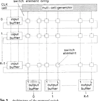
switch element array
-
-C L K cell , .I null- cel I generotor
I
0 1
Fig. 1 Architecture of the proposed switch
1 L
output butter
~ 7-
K-I
The concept of the distributed-knockout switch was introduced in [l], where a recursive high-capacity rnod- ular switch was proposed. In that design, buffers were provided at the output port, and it
was
shown that, hardware complexity could be reduced significantly in comparison with the original knockout switch. A mod- ification with input and output buffers was studied in[7]. However, in [7], the authors only evaluated the per- formance without proposing any architecture. In this paper, we present a feasible architecture of the distrib- uted knockout switch by chaining the rightmost switch elements to input ports. In the modified switch archi-
I49
tecture, a cell which loses contention can retry immedi- ately in the next time slot. A priority scheme is adopted to preserve cell sequencing. Performance of the pro- posed switch is evaluated by computer simulations. 2 Switch architecture and its operation
Fig. 1 shows the architecture of the proposed switch. It is similar to the distributed knockout switch studied in [I]. The major difference is that the output of each rightmost switch element is connected back to the input port. A consequence of this feedback design is that a cell which loses contention is not dropped. Instead, it reaches a different input port and can contend for the desired output port in the next slot.
cross state toggled state
or a n d
A V J A i l A w A n
pw 5 P" pw
'
P"Fig. 2 Functional diagram of the switch element
The operation of the switch elements is identical to that of the switch elements proposed in the recursive modular switch [l] and is illustrated in Fig. 2. and
P,
indicate, respectively, the address and the priority of cells input from the west side, A , and P, cells input from the north side. Each switch element can only be in the cross or the toggled state. If A , # A , or P,< P,,
the switch element is in the cross state and routes cells from the west side to the east side, and cells from the north side to the south side. If A,, = A,, andP,,
>P,,,
the switch element is in the toggled state and routes cells from the west side to the south side and cells from the north side to the east side.
To describe the routing mechanism, an example of a 4 x 4 switch with L = 2 is illustrated in Figs. 3-5, where L represents the maximum number of cells which can be received in a slot per output port. For simplicity, the cell body is not shown in these Figures. The buffer at each input port is partitioned into an upper buffer and a lower buffer. Note that, unlike the recursive modular switch, a cell which loses contention is routed to a different input port and is stored in the lower buffer of that input port. The upper buffer is for storing cells which arrive at the input port. An input port will always send the cell in the lower buffer, if nonempty at the beginning of a slot. If the lower buffer is empty, the cell at the head of line of the upper buffer is transmitted. In Fig. 3, the cells to be transmitted by input ports 0, 1 and 2 are all destined to output port 1 at the beginning of time slot n. Since L = 2, only two cells out of the three can reach output port 1 at the end of time slot n. In this example, the cell transmitted by
input port 0 is delivered to the lower buffer of input port 2 for transmission in time slot n
+
1. The head of line cell of input port 3 is routed to its destination out- put port 2 without any contention because only this cell is destined to output port 2 in time slot n. The results at the end of time slot n are shown in Fig. 4.0 0 1 1 2 2 3 3 b u f f e r OW 4 x 8 switch- element array Output I 1 0 1 2 3
Opeiarion ofa 4 x 4 switch with L = 2 beginning of time slot n Fig.3 buffer) element output array buffer
,
I 0 1 2 3Fig.4 Operation of a 4 x 4 switch with L = 2 end of time slot n
Fig.5 Operation of a 4 x 4 switch with L = 2: end of lime slot n + I
T o preserve cell sequencing, the priority of a cell which reaches an input port is increased by one. For example, as shown in Fig. 4, the priority of the cell which reaches the lower buffer of input port 2 is increased by 1 and this cell will be transmitted in time
IEE Proc -Cornmu, , Vol 143, No 3, June I996
slot n + 1. The results at the end of time slot n
+ 1 are
shown in Fig. 5. With the feedback design, maintaining a desired cell-loss probability, the value of L and the hardware complexity can be significantly reduced. The detailed design of switch elements was considered in [l]. In Section 3 we present the design details of the input-port controller.3 Design of input-port controller
The input-port controller shown in Fig. 6 consists of a control logic circuit, a priority incrementer, two skew D-type flip-flops, a write-control circuit, two serial-to- parallel converters (SIP), a parallel-to-serial converter (PIS), and two buffers, where the lower-buffer size is one cell and the upper-buffer size is eight cells. The control logic and the priority incrementer of the input- port controller should perform the following actions. ( a ) If the priority value of a cell which reaches an input port
is equal to 0
or2p
- 1, where P is the number o fpriority bits, the cell is discarded. Otherwise, the prior- ity value is incremented by one and the cell is stored in the lower buffer.
(b) If the lower buffer is not empty, the cell in the lower buffer is sent to the switch. Otherwise the head- of-line cell in the upper buffer is transmitted.
IcLK
input-buffer I 1 O D ' priority ~ incrementeri PF,I
/AF,
CLK input buffer priority in c rementeriBlock diugrum of the input-port controller Fig. 6
To meet the goal of timing synchronisation and alignment, the cells are skewed properly before they are sent to the switch. This skewing can easily be per- formed by a delay circuit (e.g. a D-type flip-flop) and buffers. Hence, the address and priority field signals of the upper input port will be delayed a clock cycle by D- type flip-flops, respectively, and then sent to the next input port so that the cells can be aligned for routing to their destination output ports via the switch ele- ments.
4 A multicast version
The proposed switch architecture can be modified to provide multicast service, as illustrated in Fig. 7. An
IEE Proc.-Commun., Vol. 143, No. 3, June 1996
additional bit for indication of multicasting, called the multicast bit, is added to the cell format. Multicast modules are provided to handle multicast cells. The function of the switch elements is modified. Define the state variable Y of a switch element as
Y = {
orM,
= 0,A,
= A, andP,
>
P,
(
1) where M , and Mn are the multicast bits of cells from, respectively the west, and north sides. A switch element is in the toggled state if Y = 0 or cross state if Y = 1. For example, the first cell of input port 3, a multicast cell, will be routed to a multicast module which will generate copies and send them to proper output ports using the bit-addressing method. The proper destina- tion output ports are stored in the look-up table. In this example, the multicast cell is copied to output ports 0, 1 and 3.0 1
ifM, = l!,M,,, = M,andP,
>
P,ifM,
# hfnorA,
# A,orP,
5
P,
0
I
output1
3
1
buffertable -..+ 0 1
multi cast controller control point-l
Fig. 7
ing controller Architecture
of a 4 x 4 Jwitch with a multicast module RC = rout-
input
I
1
K-bit shifter register ~- K-bit shifter register-
control Si(7naI1
;
I
?
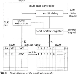
'Igna1Fig. 8 Block diagram of the multicust controller
The multicast module consists of an output buffer, a multicast controller and a look-up table. The block dia- gram of the multicast controller is shown in Fig. 8. The source address (SA) and the VPIIVCI of a multicast
cell are first extracted for determining the proper desti- nation output ports The look-up table can be imple- mented by content-addressable memory (CAM) and RAM. The CAM gives an address to read K-bit data from the RAM when the contents in the CAM are matched with the values of SA and VPIiVCI The K-bit data will then be loaded into the shift register and shifted to the control-point register in each output- buffer controller which will be described below Input cell delayed m bits will also be sent to the control point, where m is equal to K clock cycles plus the access time of the look-up table for synchronising with the control signal (CS) If the value of the control-point register is 1, the input cell is stored into the output buffer. In our example, the multicast cell will be received by output ports 0, 1 and 3 and be discarded by output port 2
With bit addressing, the multicast module can quickly generate from 2 to K copies and send them to pi oper destiiiatioii output ports The number of multi- cast modules can be selected based on the amount of multicast traffic More multicast modules are required for more multicast traffic To provide multicast service. a small switch is required at each output port The switch size is ( L
+
M ) x ( L+
M ) where L is the number of links per output port and A4 is the numberof multicast modules
control- point
reg i s t e r IDO, I D I , ID2,
-_
point
routing controller
I C input con
OD,
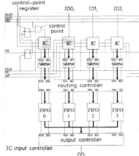
Fig. 9 Block diagram of the output-buflei contiolla
A block diagram of the output-buffer controller is shown in Fig. 9. It consists of input controllers (IC), skew buffers, FIFOs, a routing controller and an out- put controller. This output-buffer controller is shown for an output port with
L
= 3 and A4 = 1. The first input controller receives the multicast cell, and other input controllers receive unicast cells. The control sig- nal is shifted to a D-type flip-flop and latched by another D-type flip-flop which is a control-point regis- ter for storing the control signal. If the control signal is equal to 1, the multicast cell is passed to the input con- troller which detects its priority value. If the priority value of the incoming cell is equal to 0, the cell is dis- carded. Otherwise, the cell is sent to the skew buffer for cell alignment so that the four cells can be synchro- nised. The routing controller, which is a small switch, isI52
used to route input cells to the FIFOs in a round-robin fashion so that the FIFOs can be used fairly to reduce the cell-loss probability. The output controller serves the four FIFOs sequentially.
5 Performance evaluation
Approximate analysis of a nonblocking switch with input and output buffers has been provided previously [7-91. Unfortunately, results obtained from approxi- mate analysis are not very accurate. Moreover, our proposed switch does not fit the model analysed in [7- 91. For example, the lower buffer of the uppermost input port is always empty. Also, with the function defined for each switch element, an input port in an upper position has a higher priority than an input port in a lower position. Therefore, in this Section we present the performance of our proposed switch archi- tecture obtained from computer simulations.
1 0 7 -0 9 0 8 c 3 Q L Y O 7
c
5 0 6 0 5 0 4 0 4 0 5 0 6 07 0 8 0 9 1.0 offered loadThroughput of a 32 x 32 switch f o r K = 32, B, = 32 and Bo =
Fig. 10 32, 95% confidence interval -9- L = 1 ..- -0- - - L = 2 - - 0 - - - L = 3 _ _ A - - L = 4
Assume there are B, cells in the upper buffer of an input port and Bo cells in the output buffer. We simu- late the proposed switch with
L
= 1 to L = 4. Consider first the uniform-traffic model, i.e. cells are generated independently with identical probabilities by input ports and each cell is equally likely destined for every output port. The throughput of a 32 x 32 switch under different traffic loads is shown in Fig. 10. The maxi- mum throughput forL
= 1 is less than 0.6 and the maximum throughput for L 1 3 is close to 1. In the simulations, both B, and Bo were set to 32 cells. There- fore, L = 3 approaches an output-queued switch and thus should be a good choice.The cell-loss probability for different input buffer sizes is shown in Fig. 11. The simulation results were obtained at an offered load of 0.8 and Bo = 32 cells. From the results one can see that, for L = 3, an input buffer size of eight cells is enough to achieve a cell-loss probability of no more than at an offered load of 0.8. To determine the proper number of priority bits, we simulated the proposed switch with various num- bers of priority bits. The results are shown in Fig. 12. It can be seen from Fig. 12 that two bits are enough for the priority field.
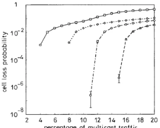
Let us consider now the cell-loss probability under the hot-spot nonuniform-traffic model. Suppose that there is a hot output port which attracts h% traffic
from all input ports. The rest 1 - h% traffic is destined to all output ports with equal probability. We simu- lated the original knockout switch and our proposed switch and the results are shown in Fig. 13. It can be seen that our proposed switch can handle the investi- gated hot-spot nonuniform traffic much better than the original knockout switch.
e.- ... 0 . - ...
1.
. I . . . . . . . .e - . . .I
1
J
2 4 6 8 10input buffer size (cells)
Fig. 1 1 Relationship between cell-loss probability and input buflkr size for K = 32 and B = 32 at 0.8 offered load, 95% confidence interval
-n- L = ? - - - 0 - - - L = 2 - _ _ 0 - - L = 3 -- A-- L = 4
I
A
X
z
Q!
-s
10-F:
1
10-8I
0.5 0.6 0.7 0.8 0.9 1.0 ottered loadFi .12 Relationship between cell-loss probability and offered load for d a r e n t numbers ofpriority bits for K = 32, E, = 8, E, = 32, and L = 3, 95% confidence interval -0- P = I - -
-o---
p = 2 - - 0-- P = 3 ..~ -A- - p = 4 l o - * I I 0 0.1 0.2 0.3 0.4 0.5 h o t - s p o t rate, %Fig. 13 Comparisons between the knockout switch ( K S ) and the pro- posed switch ( P S ) ; fo r the KS, E, = 0 und Bo = 40: for the PS, E, = 8 and
Bo = 32, 95% conzdence interval -0- KS, L = 1 _ _ _ 0--- KS, L = 2 - -
o-..
-- K s L = 3 _ _ _ a- - KS, L = 4 2 4 6 8 10 12 14 16 18 20 percentage of multicast trafficFig. 14 Relutionship between cell-loss probability and percentuge of mul- ticast trafiic for various numbers ofmulticast modules for K = 32, L = 3, C
= 2, B . = 32, E , = 64 und E, = 32 at 0.8 offered load, 95% conjidence inteyvaf -0- M = 1 ---0--- M = 2 - - O - - M = 3 - - A - - M = 4 4
a
12 16 20 24 28 32multicast buffer size (cells)
Fig. 15
size for various percentages of multicast traficjor K
C = 2, E, = 32, and B, = 32 ut 0.8 offered lud,'95%confidence interval -0- R = 1
- - 0 - - R = 3 - - A - - R = 4
Relationship between cell-loss probability and multicast bufler 32, L = 3, A4 = 1, ---0--- R = 2 2\ c .- 3 lo-* 0 n 0, CL -
2
10-4 8 16 24 32 40 48 56 64 output butter size (cells)Fig. 16 Relationship between cell-loss probability and output buffer size for various numbers of copies for K = 32, L = 3, M = I , R = 3, B, = 32 and E, = 32 at 0.8 offered loud, 95% confidence interval
-0-
c
= 1---0--- c = 2
- -
o--
c = 3- - a - - c = 4
In Figs. 14-16 are plotted the results for multicast services. It is assumed that all multicast cells generated by a particular input port have the same distributions for the number of copies, and the destinations of the copies are uniformly distributed over the output ports.
153
When the buffer of an output port is full, an arriving cell is discarded. A multicast cell is discarded if the buffer of the multicast module is full. Every discarded cell is counted once (no matter whether it is lost by a multicast module or an output port) in computing the cell-loss probability. It is clear that more multicast modules are required for a higher percentage of multi- cast cells. To determine the conditions on the number of multicast modules to achieve stability, we define the following variables:
K = number of ports in the switch M = number of multicast modules
pi = probability of arrival of a cell in a time slot on input i
pu = probability of arrival of a unicast cell to an output port in a time slot
pm = probability of arrival of a multicast cell in a time slot
Ri
= probability that a cell which arrives at input i is a multicast cellCi
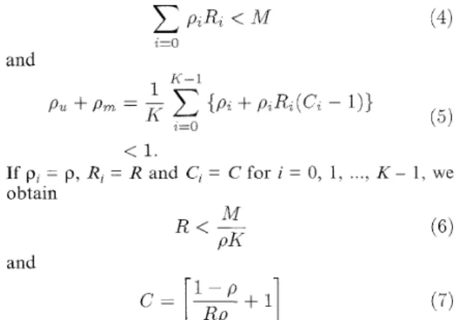
= average number of copies requested by a multicast cell generated by input iFrom the above definitions, we can obtain
and
1 K - l
Pm = - P,R,C,
a=O
K
For the proposed switch to be stable (assuming that B,
= Bo = -), the following two constraints have to be satisfied: K-1 and i=O
.
K-I (4)<
1. If pi = p, R, = R a n d C, = C f o r i = 0, 1, ..., K - 1, we obtainM
R < -
PK andc =
[-+I] 1 - Pwhere
[XI
represents the largest integer smaller than or equal tox.
The above equations give the conditions on the minimum number of multicast modules. For exam- ple, if the percentage of multicast traffic is 80% at p = 0.8 for K = 32, then 21 multicast modules are required. If there is only one multicast module, the percentage of multicast traffic must be under 3.9% at p = 0.8. Simi- larly, the average number of copies is at most eight cells under a 3% multicast traffic at p = 0.8.From the results obtained from unicast traffic, L = 3 was chosen for the study of the system performance for multicast service. The relationship between cell-loss probability and the percentage of multicast traffic using various numbers of multicast modules is shown in
154
Fig. 14. To achieve a low cell-loss probability, say lo-’, the conditions defined by eqns. 6 and 7 must be satis- fied.
The required multicast-buffer size is determined by the percentage of multicast traffic. The relationship between cell-loss probability and multicast-buffer size under various percentages of multicast traffic is shown in Fig. 15. It can be seen that the cell-loss probability decreases slightly as the multicast-buffer size increases when the percentage of multicast traffic is greater than or equal to 4%. If the percentage of multicast traffic is less than or equal to 3%, a multicast buffer of 18 cells is enough to obtain a cell-loss probability of no more than at an offered load of 0.8. The required out- put-buffer size is determined by the number of copies. The relationship between cell-loss probability and out- put-buffer size for various numbers of copies is shown in Fig. 16. If the average number of copies is less than or equal to 4, the output-buffer size can be limited to only 44 cells, and
a
cell-loss probability of no more than at an offered load of 0.8 will still be obtained.6 Conclusions
A nonblocking ATM switch has been designed based on the distributed-knockout principle. The design greatly simplifies the complexity with feedback links to chain the rightmost switch elements to input ports. As opposed to the original distributed knockout switch studied in [I], the proposed switch only drops cells which lose contention for a set consecutive number of times. With a simple priority scheme, the proposed switch is capable of preserving cell sequencing. The maximum throughput of the proposed switch was shown to be close to 1 when the number of links per output port is greater than or equal to 3. With a little modification, the proposed switch can provide multi- cast services. 7 1 2 3 4 5 6 7 8 9 10 References
CHAO. H.J.: ‘A recursive modular terabitkecond ATM switch’, IEEE J . Select. Areas Commun., 1991, 9, (8), pp. 1161-1172
JENQ, Y.C.: ‘Performance analysis of a packet switch based on a
jingle-buffered banyan network’, IEEE J. Select. Areas Commun., 1983, 1, ( 6 ) , pp. 1014-1021
HUI, J.Y., and ARTHURS, E.: ‘A broadband packet switch for integrated transport’, ZEEE J. Select. Areas Commun., 1987, 5 ,
pp. 12661273
KOZAKI. T., ENDO, N., SAKURAJ, Y., MATSUBARA, O., MIZUKAMI, M., and ASANO, K.: ‘32 x 32 shared buffer type ATM switch VLSI’s for B-ISDN’s’, IEEE J. Select. Areas Com-
~ 1 7 . . 1991, 9, (8), pp. 1239-1247
YEH. Y.S.. HLUCHYJ, M.G., and ACAMPORA, A.S.: ‘The knockout switch: A simple, modular architecture for high-per- formance packet switching’, IEEE J. Select. Areas Commun., 1987, 5. (8), pp. 12741283
HLUCHYJ, M.G., and KAROL, M.J.: ‘Queueing in high-per- formance packet switching’, IEEE J. Select. Areas Comnzun., 1988, 6, (9), pp. 1587-1597
SUH, J.J., and JUN, C.H.: ‘Performance analysis of the knock- out switch with input buffers’, IEE Proc. Commun., 1994, 141,
( 3 ) , pp. 183-189
KAROL, M.J., HLUCHYJ, M.G., and MORGAN, S.P.: ‘Input versus output queuing on a space-division packet switch’, IEEE Trans., 1987, COM-35, (12), pp. 1347-1356
OIE, Y., MURATA, M., KUBOTA, K., and MIYAHARA, H.: ‘Performance analysis of nonblocking packet switch with input and output buffers’, IEEE Trans., 1992, C O M 4 0 , (8), pp. 1 2 9 6 1297
ENG, K.Y., HLUCHYJ, M.G., and YEH, Y.S.: ‘Multicast and broadcast services in a knockout packet switch’. Proceedings of IEEE INFOCOM’88, 1988, pp. 29-34
![Fig. 1 shows the architecture of the proposed switch. It is similar to the distributed knockout switch studied in [I]](https://thumb-ap.123doks.com/thumbv2/9libinfo/7571145.125229/2.920.489.802.149.956/architecture-proposed-switch-similar-distributed-knockout-switch-studied.webp)