Both the proposed filters possess transmission zeros at out band for suppressing unwanted signals. A double-pole double-throw bare die transmitting/receiving switch is mounted on the surface of the substrate. The interconnection between the bare die switch and the buried circuits is established by bond wires. The effect of the bond wire is considered by incorporating its equivalent inductance into the design of the filters. The overall size of the antenna front-end module is only 6.2 mm 5.4 mm 0.98 mm with most of the space (near two-thirds of the volume) reserved for the antenna so as to have a better radiation performance. Also, to avoid the potential close proximity coupling among the buried circuits and the antenna, numerous metal vias connecting the top and bottom grounds in the module are designed for shielding. Since the radiation of a small antenna is influenced by the nearby circuit ground due to induced ground current, the developed antenna front-end module is tested on two FR4 printed circuit boards (PCBs) with different sizes (i.e., 55 mm 20 mm and 80 mm 46 mm). It is demonstrated that the antenna module performs well on these two grounded PCBs. The achieved 10-dB return-loss bandwidths are near 900 MHz for the transmitting and receiving paths. The measured radiation patterns are quite omnidirectional with peak gains (including the losses of circuit components) at approximately 0 dBi for the transmitting path and
1.7 dBi for the receiving path.
Index Terms—Inverted-F antenna, low-temperature co-fired ce-ramic (LTCC), RF front-end module, system-on-package (SOP), wireless local area network (WLAN).
I. INTRODUCTION
R
ECENTLY, the wireless local area network (WLAN) sys-tems have been widely used in handheld devices such as notebooks and personal digital assistants (PDAs). The size and weight of the components are important factors in the product development. The “system-on-package” (SOP) is an important concept to implement a miniature circuitry, which integrates many active and passive devices of a functional system or Manuscript received February 13, 2008; revised June 09, 2008 and August 19, 2008. First published October 24, 2008; current version published November 07, 2008. This work was supported in part by the National Science Council, R.O.C., under Contract NSC 96-2752-E-009-003-PAE.C.-C. Weng and S.-J. Chung are with the Department of Communication En-gineering, National Chiao Tung University, Hsinchu 30050, Taiwan (e-mail: chiachunweng@hotmail.com; sjchung@cm.nctu.edu.tw).
C.-F. Chang was with the Department of Communication Engineering, National Chiao Tung University, Hsinchu 30050, Taiwan. He is now with the Realtek Semiconductor Corporation, Hsinchu 30076, Taiwan (e-mail: rickycfc@msn.com).
Digital Object Identifier 10.1109/TMTT.2008.2005889
sity switches) and buried passive devices (low-pass filters, bandpass filters, baluns, diplexers, matching networks, and even antennas) into a package. The LTCC technology is used widely in multilayer substrate for designing a miniature RF passive component, due to low tolerance in dielectric constant, high degree of integration, and feasibility for multilayer circuit design.
In this study, we develop an RF front-end antenna switch module using LTCC, which is to be applied in the IEEE 802.11a WLAN. Following the IEEE 802.11a standard, the RF front-end modules using LTCC technology have been presented in [3]–[6], where only the filters and active devices were integrated in the module. Different from the authors’ prior works, the RF front-end antenna switch module proposed here possesses a higher integration level, including not only the passive circuit components (a bandpass filter and low-pass filter) and active device (a double-pole double-throw (DPDT) T/R switch), but also an embedded antenna.
Although the LTCC-based antenna front-ends have been pub-lished in recent years, most of them operated at the millimeter-wave frequency [7]–[9]. The component design and circuit in-tegration were straightforward, resulting in a large module size as compared to the wavelength. For the microwave application, due to the long wavelength, the module needs to be designed in a miniature size. This implies that the buried components would be crowded in the high dielectric-constant material. The coupling among circuits and the antenna should thus be care-fully handled to retain each component’s function. Recently, a microwave antenna integrated LTCC module has been devel-oped for the Bluetooth application [10], which achieved a com-pact size (12 mm 12 mm), as compared to the wavelength at 2.4 GHz. However, the antenna performance, especially the ra-diation pattern, was not checked. The influence of the size of the printed circuit board (PCB) on the antenna characteristics was also not considered.
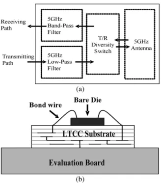
The block diagram of the 5-GHz antenna switch module to be developed in this paper is shown in Fig. 1(a). The two filters and the antenna are buried in the LTCC substrate, while the bare-die DPDT T/R switch is mounted on the top surface of the LTCC substrate. Note that for suppressing the harmonic signals from the power amplifier (not included in the present module) while remaining a minimum insertion loss, a low-pass filter, instead of a bandpass filter, is used in the transmitting path.
The interconnection between the switch and antenna, as well as that between the switch and buried circuits, are established 0018-9480/$25.00 © 2008 IEEE
Fig. 1. (a) Block diagram of the proposed RF front-end antenna switch module. (b) Side view of the bare die, bond wires, and buried circuits.
by bond wires, as shown in Fig. 1(b). Since the bond wire be-haves as an inductor in the high-frequency range, we have to take its effect into consideration [11]–[13] so as to improve the impedance matching of the buried circuit. In this paper, we consider the effect of the bond wire by incorporating it into the design of the bandpass filter and low-pass filter. The fil-ters were designed and simulated using Ansoft Corporation’s full-wave electromagnetic (EM) High Frequency Structure Sim-ulator (HFSS) simSim-ulator [14] and Applied Wave Research Inc.’s Microwave Office circuit simulator [15]. The experimental and simulation results are presented in each section.
II. DESIGN OFCOMPONENTS
The receiving path of the 5-GHz antenna switch module is composed of an antenna, a DPDT switch, and a bandpass filter, while the transmitting path is composed of a low-pass filter, the DPDT switch, and the antenna. There are 14 layers (seven thin layers and seven thick layers) used in the LTCC substrate for all the components.
In the development of the antenna switch module, there were totally four types of the LTCC modules fabricated for the test purpose. The four modules contain all the buried components (i.e., the bandpass filter, low-pass filter, and antenna), but with different output ports. Modules 1 and 2 have two output ports, which were built for testing the performances of the bandpass filter and low-pass filter, respectively. The two output ports of these modules were connected to the filter ports by additional 50- lines in the LTCC. All the other components were left floating. Fig. 2 presents the photograph of the test fixture for modules 1 and 2. Module 3 was fabricated for antenna testing, which has a single output port connected to the buried antenna in the LTCC. Note that although without the DPDT switch in these three modules, the bond wire associated with each passive
Fig. 2. Test fixture for modules 1 and 2.
TABLE I
FOURRF FRONT-ENDMODULES FORTESTING
Tx= Transmitting Path, Rx = Receiving Path.
component was reserved since its effect had been considered in the component design. Finally, module 4 is the complete an-tenna switch module including the buried passive components, the DPDT switch, and the connecting bond wires. This module has three output ports, the first corresponding to the transmitting path, the second to the receiving path, and the third reserved for an external antenna for diversity application. Table I sum-marizes the four types of the modules. More details about the modules will be revealed in the following.
A. Bandpass Filter
The proposed bandpass filter uses inductors as the impedance transformer at the I/O ports instead of capacitors in most band-pass filter configurations [16]–[19]. The inductor can be imple-mented by an external bond wire or internal buried circuits.
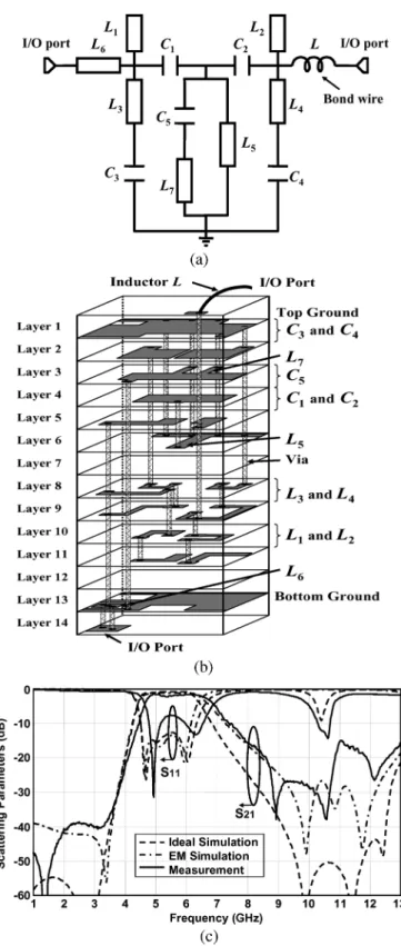
The schematic of the new bandpass filter for the module is shown in Fig. 3(a). It is a third-order filter with one parallel
LC resonator (formed by striplines and and capacitor ) and two equivalent parallel LC resonators, which are com-posed of two series LC resonators ( , , and , ) and two open-end stripline stubs . The two series LC resonators can provide finite transmission zeros at lower frequencies. In the passband, these resonators behave as inductors, which are shunt to the two capacitive striplines and , thus generating two transmission poles. In addition, the striplines and are open-end stubs with different length, which are quarter-wave-length resonators providing two transmission zeros at higher fre-quencies (near the second harmonics of the operating frequen-cies). Moreover, the series LC resonator can provide the third transmission zero at a higher frequency.
Fig. 3. (a) Schematic of the proposed bandpass filter. (b) 3-D layout of the bandpass filter. (c) Simulated and measuredS-parameters of the bandpass filter.
The capacitors and are admittance inverters used to control the coupling between the LC resonators and act together with and as dc-decoupling capacitors to block the dc signals before and after the filter. The stripline acts as an impedance transformer matching the resonators to the external
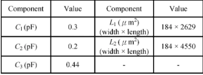
impedance, as does the inductor . Notably, the inductor (ap-proximately 1 nH) is not buried in the LTCC substrate, but im-plemented utilizing an external bond wire, which is used to con-nect the bandpass filter and the top-surface bare die (the DPDT T/R switch). The corresponding component values are listed in Table II.
The 3-D layout of the bandpass filter is shown in Fig. 3(b). 14 layers are used. The thicknesses of the first layer and the eighth to thirteenth layers are all equal to 0.09 mm, and those of other layers are 0.04 mm. The bandpass filter was fabricated in module 1 using the Dupont 951 LTCC process with a substrate dielectric constant of 7.8. The commonly used FR4 PCB with a dielectric constant of 4.4, loss tangent of 0.02, and thickness of 0.8 mm, is used as the evaluation board (Fig. 2) for measuring the performance of the fabricated LTCC filter.
The measured -parameters, as well as the ideal circuit simulation and EM simulation results, are shown in Fig. 3(c). The measured results agree with the EM simulations, but exhibit only two poles in the passband due to the inaccuracy of the LTCC process. The inaccuracy also deteriorates the return loss in the passband and results in the discrepancy between the measurement and simulation in the higher stopband. The reason for the inaccuracy is that during the LTCC firing process, there is tape shrinkage between 10%–5% occurring in the length and width dimensions and slightly in the height. It will change the capacitance and inductance in the LTCC module and cause the discrepancies between the EM simulation and measurement. Nevertheless, the measured insertion losses from 4.85 to 6 GHz are less than 2.31 dB with a minimum value of 1.5 dB at 4.92 GHz. Both the transmission zeros at the higher frequen-cies of 8.92 and 10.5 GHz provide suppression near 38 dB. In addition, the suppression in the range of 1–3 GHz is higher than 38.7 dB.
B. Low-Pass Filter
The schematic of the proposed low-pass filter incorporating the bond wire is shown in Fig. 4(a). The low-pass filter has six elements with two transmission zeros in the stopband. The inductor was implemented utilizing the external bond wire, which was used to connect the low-pass filter and the top-surface bare die (the DPDT T/R switch). Since the short stripline of low characteristic impedance can be represented by a T-equiva-lent circuit [20], as shown in Fig. 4(b), the stripline in shunt
Fig. 4. (a) Schematic of the proposed low-pass filter. (b) Equivalent circuit of the low-pass filter.
TABLE III
CORRESPONDINGCOMPONENTVALUES FOR THELOW-PASSFILTER
with the capacitor would be resonant at two higher frequen-cies, thus producing two transmission zeros. By changing the length of the stripline or the value of the capacitor , we can control the frequency locations of the two zeros. The corre-sponding component values are listed in Table III.
The 3-D layout of the proposed low-pass filter is shown in Fig. 5(a). Since the filter has only five buried elements, we use three layers (eighth to tenth layers) for this layout. In order to reduce the fabrication inaccuracy affecting the filter perfor-mance, the thick layers were used for enhancing the capacitance tolerance.
The measured results with a bond wire (using module 2) are depicted in Fig. 5(b). The simulation results are also shown for comparison. There is a small discrepancy between the measure-ment and simulation in the higher stopband due to the inaccu-racy of the LTCC process. The measured insertion losses from 4.9 to 6 GHz were less than 1.57 dB with a minimum value of 0.95 dB at 5.3 GHz. Moreover, the transmission zeros at
Fig. 5. (a) 3-D layout of the low-pass filter. (b) Simulated and measured S-pa-rameters of the low-pass filter.
10.3 and 12.4 GHz provide suppressions of 35.6 and 41.4 dB, respectively.
C. DPDT T/R Switch
A DPDT T/R switch is used to switch the antenna port to the bandpass filter or the low-pass filter for receiving or transmit-ting signals, respectively. The requirement of the switch is low insertion loss at operating band and high rejection between the through and isolation ports. In order to miniaturize the entire module, a GaAs pseudomorphic HEMT (pHEMT) monolithic microwave integrated circuit (MMIC) DPDT bare die switch [21] is used for the module integration. The size of the bare die switch is 0.99 mm 0.93 mm. The insertion loss and isolation at the operating frequencies (4.85–6 GHz) are around 1 and 25 dB, respectively.
D. Embedded 5-GHz Antenna
An embedded 5-GHz antenna was designed in the LTCC multilayer substrate. The antenna is required to have input impedance near 50 for good return loss and possess proper antenna gain (with peak gain larger than 0 dBi). The radiation
Fig. 7. (a) Geometry of the small PCB containing the antenna switch module. (b) Size of the 5-GHz antenna in the LTCC module. Ant. Feed= antenna feed.
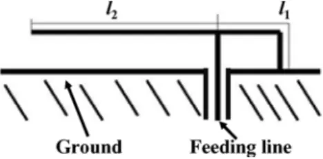
patterns should be as omnidirectional as possible at the op-erating frequencies. The antenna designed for this module is based on the inverted-F antenna shown in Fig. 6, where and are the lengths of the short- and the open-circuited strips. For resonance, the electrical length of should be near 90 at the operating frequency [22].
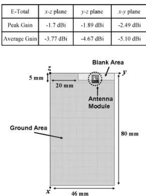
The present antenna switch module is proposed for use on a small FR4 PCB with size of 55 mm 20 mm (the typical size for a USB dongle) in which the substrate ground occupies an area of 50 mm 20 mm 5 mm 4 mm , as shown in Fig. 7(a). The LTCC antenna module (module 3) with area of 6.2 mm 5.4 mm [see Fig. 7(b)] is to be placed on the corner of the substrate (the blank area), with the circuit portion (filters and
Fig. 8. EM simulated and measured return losses(1=S ) of the embedded inverted-F antenna on the PCB with size of 55 mm2 20 mm.
switch) intruding into the ground area. The antenna occupies an area of 4 mm 5.4 mm.
The EM simulator (HFSS) was used to simulate and design the 3-D LTCC embedded antenna. The resultant antenna struc-ture, as shown in Fig. 7(b), is little dissimilar to a typical in-verted-F antenna in the antenna’s right half part (including the area around the antenna feed and short end) due to the consider-ation of impedance matching. However, this area, like a conven-tional inverted-F antenna, still contributes most of the antenna’s radiation field since large induced current distributed around it. Also, in order to reduce the antenna size, the open-circuited end of the inverted-F antenna is bent downward. The antenna was built on only two layers. The bent open-circuited end was placed on the top surface of the module, and the other portion of the antenna was on the second layer, with vertical via con-necting them. We may tune the antenna resonance frequency by cutting the open-circuited end if the frequency is shifted down-ward due to the fabrication inaccuracy. The electrical length of equals 12.3 mm and the other dimensions are shown in Fig. 7(b). A -matching network on the top surface of the LTCC was reserved to match the input impedance. The M1 is the series element, and M2 and M3 are the shunt elements for the -matching network. The bond wire for connecting the an-tenna and the DPDT switch was also kept on the module before the 50- output line.
The EM simulated and measured return losses are presented in Fig. 8. The measured 10-dB return-loss bandwidth is from 4.73 to 5.95 GHz, which agrees quite well with the sim-ulated one (from 4.7 to 6.0 GHz). Fig. 9 shows the far-field nor-malized radiation patterns in the principal planes at 5.25 GHz. Both the measured and simulated results are shown for compar-ison. It is seen that they are consistent with each other and are quite omnidirectional in the – - and – -planes. The measured peak gains in the – -, – -, and – -planes are 0.35, 0.15, and 0.12 dBi, respectively. The average gains in these planes are correspondingly 1.32, 3.03, and 3.18 dBi.
III. INTEGRATION OF THEANTENNASWITCHMODULE According to the proposed bandpass and low-pass filters, we integrated these circuits and the antenna into a package and sim-ulated the coupling effect and isolation. We first pre-simsim-ulated each buried components, then put them together into a package,
Fig. 9. EM simulated and measured far-field normalized radiation patterns in the: (a)x–z-plane, (b) y–z-plane, and (c) x–y-plane at 5.25 GHz on a PCB with a size of 55 mm2 20 mm.
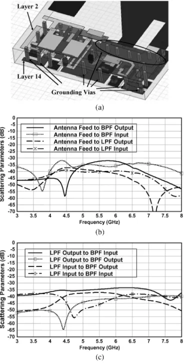
and finally fine tuned the entire antenna module. The size of this antenna switch module is merely 6.2 mm 5.4 mm 0.98 mm. 14 LTCC layers were used with seven thin layers (0.04 mm) and seven thick layers (0.09 mm). The thickness of each metal plate (silver alloy) is 0.006 mm. The second and fourteenth layers are grounding layers to shield other EM interference. As shown in Fig. 10(a), many grounding vias, connecting between the two shielding layers, were designed for equalizing the potentials of the two grounding layers and suppressing the coupling among the buried circuits. The simulated results of the couplings be-tween the antenna port, bandpass-filter ports, and low-pass-filter ports are shown in Fig. 10(b) and (c) where “BPF input” (“LPF input”) and “BPF output” (“LPF output”) denote the input and output ports of the bandpass (low-pass) filters, respectively. The isolation between the antenna and two filters, and those between the filters, are all higher than 30 dB in the frequency range from 3 to 8 GHz. The simulated results show that the EM couplings among all the components in the module have been designed with negligibly small values.
The 3-D layout of the antenna switch module (module 4) is shown in Fig. 11(a). Fig. 11(b) presents a photograph of the LTCC module and indicates the metal pads on the top surface including two dc control voltage pads (Vc1 and Vc2), three grounding pads (GND3, GND4, and GND5), and two antenna pads (pad1 and Ext. Ant.). This module contains three output ports, i.e., the transmitting port (TX port), receiving port (RX
Fig. 10. (a) Grounding vias between layers 2 and 14. (b) Couplings between the antenna and filters. (c) Couplings between the low-pass filter (LPF) and the bandpass filter (BPF).
port), and external antenna port. The 0.7-mil gold wires were used as the bond wires between the DPDT switch and pads. The -matching network was realized in between the Ant. Feed, pad3, GND1, and GND2. The SMD device (0201 size) between pad2 and pad3 is the dc-blocking capacitor. Significantly, pad1 and pad2 are connected through the buried 50- transmission line in the LTCC substrate. Separating pad1 and pad2 is to avoid the surface mount solder paste adhering to pad1 and affecting the bond wire connecting from pad1 to the switch. An external antenna port (named Ext. Ant.) is reserved for antenna diversity application from which an external antenna can be connected to
Fig. 11. (a) 3-D layout of the antenna switch module. (b) Finished antenna switch module, showing the metal pads on the top surface. GND = grounding pad, Ext. Ant. = external antenna pad, V c = dc control voltage pad, BPF= bandpass filter, LPF = low-pass filter.
Fig. 12. Antenna switch module mounting on an FR4 evaluation board with a size of 55 mm2 20 mm.
this front-end module. Fig. 12 shows a photograph of the fabri-cated LTCC antenna switch module mounting on an FR4 eval-uation board with a size of 55 mm 20 mm.
Fig. 13. Measured return loss(1=S ) in the transmitting path of the entire antenna switch module on the small PCB with a size of 55 mm2 20 mm.
Fig. 14. Measured normalized radiation patterns in: (a) the x–z-plane, (b)y–z-plane, and (c) x–y-plane at 5.25 GHz for the transmitting path on the small PCB with size of 55 mm2 20 mm.
The transmitting path is composed of the LPF, DPDT switch, and antenna. Moreover, a -matching network, which includes a series capacitor (1 pF) and shunt inductor (1 nH) on the FR4 evaluation board can improve the input impedance in the trans-mitting path. The measured return loss in the transtrans-mitting path of the entire antenna switch module is presented in Fig. 13. The frequency range of return loss larger than 10 dB is from 4.76 to 5.73 GHz (approximately 970 MHz) with a maximum return loss of 33 dB at 5.3 GHz.
The measured normalized radiation patterns of the entire an-tenna switch module on the small PCB at 5.25 GHz for the trans-mitting path are shown in Fig. 14. It is seen that the patterns are quite omnidirectional in the three principal planes. The peak
TABLE IV
PEAK ANDAVERAGEGAINS IN THETRANSMITTINGPATH ON THESMALLPCB WITHSIZEof 55 mm2 20 mm
Fig. 15. Measured return loss(1=S ) in the receiving path of the entire an-tenna switch module on the small PCB with a size of 55 mm2 20 mm.
(average) gains in the – -, – -, and – -planes are 0.24 dBi ( 2.45 dBi), 1.24 dBi ( 3.19 dBi), and 1.25 dBi ( 2.91 dBi), respectively. Table IV summarizes the results. Due to the inte-gration with the circuits, these antenna gains are varied from those described earlier.
The receiving and transmitting paths share the embedded an-tenna and DPDT switch. The bandpass filter is included in the receiving path of the LTCC substrate. In addition, a series in-ductor (1 nH) is added in the receiving path on the small FR4 evaluation board to improve the input impedance. The measured return loss in the receiving path of the entire antenna switch module is presented in Fig. 15. The bandwidth of return loss larger than 10 dB is from 4.74 to 5.63 GHz (approximately 890 MHz) with a maximum return loss of 24 dB at 5.3 GHz.
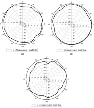
Fig. 16 shows the measured normalized radiation patterns at 5.25 GHz for the receiving path, which are also omnidirec-tional in the three principal planes. The peak (average) gains are 1.7 dBi ( 3.77 dBi), 1.89 dBi ( 4.67 dBi), and 2.49 dBi ( 5.10 dBi), respectively in the – -, – -, and – -planes. Table V summarizes the results. Due to the extra loss of the bandpass filter to the low-pass filter, the antenna gains in the receiving path are lower than those in the transmitting path.
Since the radiation of a small antenna is influenced by nearby conductors due to the induced conductor currents, the size of the grounded PCB would thus affect the radiation performance of the antenna front-end module. In order to see whether the developed antenna module can be used in a different PCB, a large PCB with a size of 80 mm 46 mm (the typical size for a PCMCIA WLAN card) was fabricated for testing. As shown in Fig. 17, the substrate ground of the large PCB occupies an area of 75 mm 46 mm 20 mm 5 mm , leaving a ground-free blank area of 26 mm 5 mm. Note that the length (26 mm) of the blank area was determined by simulation according to an
Fig. 16. Measured normalized radiation patterns in: (a) the x–z-plane, (b)y–z-plane, and (c) x–y-plane at 5.25 GHz for the receiving path on the small PCB with size of 55 mm2 20 mm.
TABLE V
PEAK ANDAVERAGEGAINS IN THERECEIVINGPATH ON THESMALLPCB WITHSIZE OF55 mm2 20 mm
Fig. 17. Geometry of the large FR4 PCB containing the antenna switch module.
optimal radiation pattern of the antenna module. A -matching network on the large PCB with a shunt inductor (2.7 nH), a series
Fig. 18. Measured return loss(1=S ) in the transmitting path of the entire antenna switch module on the large PCB with size of 80 mm2 46 mm.
Fig. 19. Measured normalized radiation patterns in the: (a) x–z-plane, (b)y–z-plane, and (c) x–y-plane at 5.25 GHz for the transmitting path on the large PCB with a size of 80 mm2 46 mm.
resister (0 ), and a shunt capacitor (0.3 pF) was used to improve the input impedance.
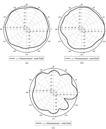
Fig. 18 shows the measured return loss in the transmitting path of the entire antenna switch module on the large PCB. The 10-dB return-loss bandwidth is 857 MHz, ranging from 4.962 to 5.819 GHz. The measured normalized radiation patterns at 5.25 GHz in the transmitting path of the entire antenna switch module on the large PCB are shown in Fig. 19. The radiation patterns are omnidirectional in the – -and – -planes. A radiation null of 17 dB happens at 330 in
degraded, the finished antenna front-end module still works well on the large PCB.
IV. CONCLUSION
In this paper, a compact RF front-end module using LTCC multilayer technology has been designed and realized. The module includes a BPF, an LPF, a DPDT bare die switch, and an embedded inverted-F antenna, and has a very small size of 6.2 mm 5.4 mm 0.98 mm. The effect of the bond wire has been taken into account by incorporating into the design of the filters. Both the proposed filters possess transmission zeros at out band for suppressing unwanted signals. The performances of the developed antenna front-end module on two PCBs with different sizes (55 mm 20 mm and 80 mm 46 mm) have been demonstrated. The measured radiation patterns are om-nidirectional. The return-loss bandwidth and antenna gain are enough and suitable for the IEEE 802.11a application. In the future, more circuit components, such as the power amplifier, low-noise amplifier, and RF transceiver can be integrated to the LTCC module. Dual-band components (bandpass filter, antenna, and balun) can also be designed in to achieve a com-plete RF front-end module for the IEEE 802.11 a/b/g WLAN applications.
ACKNOWLEDGMENT
The authors would like to thank the MAG.Layers Scientific-Technics Company Ltd., Hsinchu, Taiwan, for fabricating the LTCC antenna switch module and for helpful suggestions on the LTCC layouts. Moreover, much appreciation and thanks is also extended to Hexawave Inc., Hsinchu, Taiwan, for providing the DPDT T/R switch bare die. The reviewers are also appreciated for their valuable comments and suggestions.
REFERENCES
[1] J.-H. Lee, G. DeJean, S. Sarkar, S. Pinel, K. Lim, J. Papapolymerou, J. Laskar, and M. M. Tentzeris, “Highly integrated millimeter-wave passive components using 3-D LTCC system-on-package (SOP) technology,” IEEE Trans. Microw. Theory Tech., vol. 53, no. 6, pp. 2220–2229, Jun. 2005.
[2] S.-H. Wi, Y.-B. Sun, I.-S. Song, S.-H. Choa, I.-S. Koh, Y.-S. Lee, and J.-G. Yook, “Package-level integrated antennas based on LTCC tech-nology,” IEEE Trans. Antennas Propag., vol. 54, no. 8, pp. 2190–2197, Aug. 2006.
[3] Y.-J. Ko, J. Y. Park, J.-H. Ryu, K.-H. Lee, and J. U. Bu, “A minia-turized LTCC multi-layered front-end module for dual band WLAN (802.11 a/b/g) applications,” in IEEE MTT-S Int. Microw. Symp. Dig., Jun. 2004, pp. 563–566.
[4] C.-H. Lee, S. Chakraborty, A. Sutono, S. Yoo, D. Heo, and J. Laskar, “Broadband highly integrated LTCC front-end module for IEEE 802.11a WLAN applications,” in IEEE MTT-S Int. Microw. Symp.
Dig., Jun. 2002, pp. 1045–1048.
[5] G. Wang, M. Van, F. Barlow, and A. Elshabini, “An interdigital band-pass filter embedded in LTCC for 5-GHz wireless LAN applications,”
IEEE Microw. Wireless Compon. Lett., vol. 15, no. 5, pp. 357–359, May
2005.
[6] M.-C. Wu and S.-J. Chung, “A small SiP module using LTCC 3D cir-cuitry for dual band WLAN 802.11 a/b/g front-end solution,” presented at the Silicon Monolithic Integr. Circuits RF Syst. Conf., Jan. 2006. [7] J.-H. Lee, N. Kidera, G. DeJean, S. Pinel, J. Laskar, and M. M.
Tentzeris, “AV -band front-end with 3-D integrated cavity filters/du-plexers and antenna in LTCC technologies,” IEEE Trans. Microw.
Theory Tech., vol. 54, no. 7, pp. 2925–2935, Jul. 2006.
[8] J.-H. Lee, N. Kidera, S. Pinel, J. Laskar, and M. M. Tentzeris, “Fully integrated passive front-end solutions for aV -band LTCC wireless system,” IEEE Antennas Wireless Propag. Lett., vol. 6, pp. 285–288, 2007.
[9] D. Y. Jung, W.-I. Chang, K. C. Eun, and C. S. Park, “60-GHz system-on-package transmitter integrating sub-harmonic frequency amplitude shift-keying modulator,” IEEE Trans. Microw. Theory
Tech., vol. 55, no. 8, pp. 1786–1793, Aug. 2007.
[10] L. K. Yeung, J. Wang, Y. Huang, S.-C. Lee, and K.-L. Wu, “A compact LTCC Bluetooth system module with an integrated antenna,” Int. J. RF
Microw. Comput.-Aided Eng., vol. 16, no. 3, pp. 238–244, 2006.
[11] F. Alimenti, P. Mezzanotte, L. Roselli, and R. Sorrentino, “Modeling and characterization of the bonding-wire interconnection,” IEEE Trans.
Microw. Theory Tech., vol. 49, no. 1, pp. 142–150, Jan. 2001.
[12] M. A. I. Mostafa, J. Schlang, and S. Lazar, “On-chip RF filters using bond wire inductors,” in Proc. 14th Annu. IEEE Int. ASIC/SOC. Conf., 2001, pp. 98–102.
[13] J. Y. Chuang, S. P. Tseng, and J. A. Yeh, “Radio frequency characteri-zation of bonding wire interconnections in a molded chip,” in Electron.
Compon. Technol. Conf., Las Vegas, NV, 2004, pp. 392–399.
[14] High Frequency Structure Simulator (HFSS). Ansoft Corporation, Pittsburgh, PA, 2001.
[15] Microwave Office. Appl. Wave Res. Inc., El Segundo, CA, 2002. [16] L. K. Yeung and K.-L. Wu, “A compact second-order LTCC bandpass
filter with two finite transmission zeros,” IEEE Trans. Microw. Theory
Tech., vol. 51, no. 2, pp. 337–341, Feb. 2003.
[17] W. Y. Leung, K.-K. M. Cheng, and K.-L. Wu, “Multilayer LTCC band-pass filter design with enhanced stopband characteristics,” IEEE
Mi-crow. Wireless Compon. Lett., vol. 12, no. 7, pp. 240–242, Jul. 2002.
[18] C.-F. Chang and S.-J. Chung, “Bandpass filter of serial configuration with two finite transmission zeros using LTCC technology,” IEEE
Trans. Microw. Theory Tech., vol. 53, no. 7, pp. 2383–2388, Jul. 2005.
[19] K.-C. Lin, C.-F. Chang, M.-C. Wu, and S.-J. Chung, “Dual-bandpass filters of serial configuration using LTCC technology,” IEEE Trans.
Mi-crow. Theory Tech., vol. 54, no. 6, pp. 2321–2328, Jun. 2006.
[20] D. M. Pozar, Microwave Engineering, 2nd ed. New York: Wiley, 1998.
[21] “HWS411 GaAs DC-6 GHz DPDT Switch V3,” Hexawave Inc., Hsinchu, Taiwan, Oct. 2004. [Online]. Available: http://www.hw. com.tw/
[22] Y.-S. Wang, M.-C. Lee, and S.-J. Chung, “Two PIFA-related miniatur-ized dual-band antennas,” IEEE Trans. Antennas Propag., vol. 55, no. 3, pp. 805–811, Mar. 2007.
Chia-Chun Weng was born on August 22, 1974,
in Taipei, Taiwan. He received the B.S. degree in electrical engineering from the National Yunlin University of Science and Technology, Yunlin, Taiwan, in 1999, and is currently working toward the M.S. degree in the communication engineering at the National Chiao Tung University.
He is currently involved with research on LTCC RF passive components, LTCC front-end modules, and microwave circuit design for WLAN applications.
Chun-Fu Chang was born on February 1, 1982, in
Kaohsiung, Taiwan. He received the B.S. and M.S. degrees in communication engineering from National Chiao Tung University, Hsinchu, Taiwan, R.O.C., in 2004 and 2006, respectively.
He is currently with the Realtek Semiconductor Corporation, Hsinchu, Taiwan.
Shyh-Jong Chung (M’92–SM’06) was born in
Taipei, Taiwan. He received the B.S.E.E. and Ph.D. degrees from National Taiwan University, Taipei, Taiwan, in 1984 and 1988, respectively.
Since 1988, he has been with the Department of Communication Engineering, National Chiao Tung University, Hsinchu, Taiwan, where he is currently a Professor. From September 1995 to August 1996, he was a Visiting Scholar with the Department of Elec-trical Engineering, Texas, A&M University, College Station. His research interests include the design and applications of active and passive planar antennas, LTCC-based RF components and modules, packaging effects of microwave circuits, vehicle collision warning radars, and communications in intelligent transportation systems (ITSs).
Dr. Chung was the treasurer of the IEEE Taipei Section (2001–2003) and the chairman of the IEEE Microwave Theory and Techniques Society (IEEE MTT-S) Taipei Chapter (2005–2006). He was the recipient of the 2005 Out-standing Electrical Engineering Professor Award presented by the Chinese In-stitute of Electrical Engineering and the 2005 Teaching Excellence Award pre-sented by National Chiao Tung University.