Chemical vapor deposition of tantalum carbide and carbonitride thin
films from Me
3CELTa(CH
2CMe
3)
3(E ~ CH, N){
Yu-Hsu Chang, Jin-Bao Wu, Pei-Ju Chang and Hsin-Tien Chiu*
Department of Applied Chemistry, National Chiao Tung University, Hsinchu, Taiwan 30050, R. O. C. E-mail: [email protected]
Received 20th August 2002, Accepted 6th November 2002
First published as an Advance Article on the web 28th November 2002
Chemical vapor deposition (CVD) of thin films employing Me3CCHLTa(CH2CMe3)3and
Me3CNLTa(CH2CMe3)3as the precursors has been carried out. TaC and TaCN films were deposited at
relatively low temperatures (623–923 K). In comparison, using Me3CNLTa(CH2CMe3)3, the TaLN bond did
not undergo cleavage during the reaction and the N atom was incorporated into the film as nitride. The volatile components evolved were collected and examined by GC–MS, FT-IR,1H and13C NMR spectroscopy. Possible decomposition pathways of the tantalum complexes are proposed to rationalize the observation.
Introduction
Early transition metal carbides and nitrides have many potential applications1–2 due to their special properties, such as extreme hardness, high resistance to corrosion and oxidation, and high melting points. Recently, they have been explored as potential diffusion barriers in VLSI metalization.3 In many cases, thin films of the carbides and nitrides have been grown by MOCVD (metal–organic chemical vapor deposition) at relatively low temperatures. For example, thin films of the carbides of Ti, Zr, Cr, and W have been deposited using Ti(CH2CMe3)4,4–6Zr(CH2CMe3)4,7Cr(CH2CMe3)4,8–10
and Me3CCMW(CH2CMe3)3,11,12 respectively. Deposition of
nitride thin films has been reported employing metal complexes with organo-amido and organo-imido ligands as the precur-sors.13–19These include the deposition of nitrides of Ti from
Ti(NEt2)4, 13–15
of Ta fromtBuNLTa(NEt2)3, 16
and of W from (tBuNL)2W(NHtBu)2.17,18 In addition to the activation and
elimination pathways of the hydrocarbon fragments of the complexes, the role of the multiply bonded carbene, carbyne and imido ligands are frequently discussed. Apparently, the multiply bonded ligands may assist the preservation of ‘MLC’ and ‘MLN’ fragments in the films to form carbides and nitrides. In this study, we wish to explore the possibility of employing the Schrock’s alkylidene complex, Me3CCHL
Ta(CH2CMe3)3,20 and a closely related new imido complex,
Me3CNLTa(CH2CMe3)3,21 as the CVD precursors to grow
thin films. The precursors have isoelectronic ligands, Me3CCHL and Me3CNL, linked to the Ta center through
multiple bonds. Also, each has three neopentyl ligands that resist the low energy b-hydrogen elimination decomposition pathway. The discoveries are discussed below.
Experimental
All solvents were purchased from Aldrich. They were dried and distilled under a nitrogen atmosphere before use. The chemicals for syntheses were also purchased from Aldrich and used without further purification. Me3CCHLTa(CH2CMe3)3
was synthesized according to the literature.20 Me 3CNL
Ta(CH2CMe3)3 was a solid compound and was synthesized
from Me3CNLTaCl3py222 and Me3CCH2MgCl in hexane.21
Deposition was carried out in a homemade cold-wall low-pressure chemical vapor deposition system with a base low-pressure of ca. 1023Pa. The conditions of deposition are summarized in Table 1.
The precursor container was maintained at 318 or 338 K while the precursors were in the solid phase. During the deposition, the precursor feed line was maintained at a temperature 10 K higher than the precursor container. The flow rate of the carrier gas, Ar or H2(99.99%), was controlled
accurately and measured by a flow meter (KOFLOC, RK1400). n-Type Si(100) and quartz substrates (1.0 6 1.0 cm2) were cleaned and used for the deposition. After the feeding of the precursors was ceased, the samples were annealed at the deposition temperature for 30 min.
The films were characterized by several methods described below. XRD (X-Ray diffraction) studies were carried out using a MAC MXP-3 diffractometer with Cu-Ka1 radiation. SEM (scanning electron microscopy) images were taken by using Hitachi S-4000 and JEOL JSM-6330F instruments. AFM (atomic force microscopy) images were obtained using a Digital Nanoscope E. The XPS (X-ray photoelectron spectroscopy) measurements were carried out using a Perkin-Elmer PHI-1600 spectrometer with Mg Ka (1253.6 eV) radiation. The AES (auger electron spectroscopy) depth profile of the film was determined using a Perkin PHI-670Xi spectrometer. EPMA (electron probe X-ray microanalysis) studies were carried out using a JEOL 8900R instrument. The volatile products were analyzed with a Varian Unity-300 NMR (nuclear magnetic resonance) instrument, a VG Biotech Trio-2000 GC-MS (gas chromatography-mass spectrometry) spectrometer and a Perkin-Elmer System 2000 FT-IR (Fourier transform infrared spectrometer). The resistivity was evaluated using a Napson Resistage KG-80 four-point probe measurement system.
Results and discussion
Thin films grown from Me3CCHLTa(CH2CMe3)3
The surface morphology of the films was characterized by SEM and AFM. Smooth, good adhesion films with fine granules were observed. The deposition rate, 0.2–4.2 nm min21, was estimated from the cross-sectional SEM images. At 773 K, the growth rate was very low (0.3 nm min21). When the reaction
temperature was raised to 823 K in H2, the deposition rate
increased significantly to 4.2 nm min21. In Fig. 1, a 9 mm2AFM image of a film prepared at 623 K is shown. The surface is
{Electronic supplementary information (ESI) available: AFM and SEM images of TaC and TaCN films deposited on Si(100) at 773, 823 and 923 K. See http://www.rsc.org/suppdata/jm/b2/b208129f/
DOI: 10.1039/b208129f J. Mater. Chem., 2003, 13, 365–369 365
uniform with the Rrms(root mean square roughness) ~ 2.2 nm.
The Rrms of the surface increased from 1.6 to 5.1 nm as the
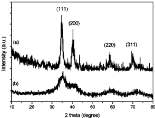
temperature of deposition was raised. The structure and crystallinity of the films were examined by XRD. It indicated that the films deposited at 623–823 K were amorphous. The XRD pattern [Fig. 2(a)] of a sample prepared at 773 K and heat-treated at 1273 K for 2 h in vacuum showed reflections at 2h ~ 34.81, 40.41, 58.61 and 69.98u, corresponding to the (111), (200), (220), and (311) reflections of a cubic material, respectively. The lattice parameter is estimated to be a ~ 0.447 nm. The value is close to the literature value of a cubic phase TaC, a ~ 0.4454 nm.23
Fig. 3 shows the AES depth profiles of a film deposited at 773 K. It indicates that the distribution of Ta, C and O within the film is uniform while the O concentration on the surface is high. Furthermore, the composition of the film was studied by XPS experiments. On the surface of a film grown at 823 K, photoelectrons of Ta, C and O were observed. The high-resolution spectra of the Ta 4f and the C 1s electrons are shown in Fig. 4. In Fig. 4(a), the signals of Ta 4f5/2 and Ta 4f7/2
electrons are observed at 25.2 and 23.3 eV, respectively. These are close to the values of TaC.24–26The major signal of the C 1s electron [Fig. 4(b)] is at 282.8 eV, indicating that the carbon atoms are in a carbidic environment. The minor signal at 284.5 eV is attributable to the presence of some graphitic carbon.27
The quantity of the carbidic carbon is estimated from the integration of the signals and is ca. six times that of the graphitic carbon. The XPS studies also showed the presence of oxygen atoms observed at 530.5 eV, which is typical for an oxidized surface.27
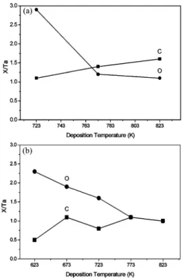
The concentrations of Ta, C and O elements in the films were estimated from EPMA measurements (Fig. 5). Using Ar as the carrier gas, the elemental ratio of C : Ta increased from 1.1 to 1.6 as the temperature was raised from 723 to 823 K, whereas the ratio of O : Ta decreased from 2.9 to 1.1. Using H2as the
carrier gas, the elemental ratio of C : Ta increased from 0.5 to 1.0 while the ratio of O : Ta decreased from 2.3 to 1.0 as the
Me3CNLTa(CH2CMe3)3 333 n-Si(100) ca. 723–923 Ar 10 sccm or H210 sccm 1–50 a
sccm: standard cubic centimeter per minute.
Fig. 1 AFM surface morphology of the film on Si(100) deposited at 623 K from Me3CCHLTa(CH2CMe3)3in H2.
Fig. 2 XRD patterns of the films on Si(100): (a) prepared from Me3CCHLTa(CH2CMe3)3at 773 K in H2and annealed at 1273 K for
2 h under vacuum, (b) prepared from Me3CNLTa(CH2CMe3)3 at
923 K in H2.
Fig. 3 Auger depth profile of the film on Si(100) deposited at 773 K from Me3CCHLTa(CH2CMe3)3in H2.
Fig. 4 High-resolution XPS spectra of the film on Si(100) grown at 823 K from Me3CCHLTa(CH2CMe3)3in Ar: (a) Ta 4f5/2and Ta 4f7/2
electrons, and (b) C 1s electrons.
J. Mater. Chem., 2003, 13, 365–369
temperature was increased from 623 to 823 K. We speculated that the films are sensitive to the oxygen and moisture in the environment. Incorporation of a high oxygen concentration into thin films has been observed frequently.11,15
A four-point probe was employed to measure the resistivity of the films. For the film deposited at 823 K under Ar, the resistivity showed the lowest value, ca. 3000 mV cm. The resistivity is high for the films deposited at low temperatures. High oxygen incorporation into the films might cause the resistivity value to be higher than the value of the TaC film prepared by PVD.28
The volatile products characterized by GC–MS, NMR and FT-IR may provide information about the reaction pathways. The volatile products were predominantly neo-pentane. Traces of isobutylene, 2,2,5,5-tetramethylhexane and 2,2,5,5-tetramethyl-3-hexene were also detected. Isobutane may also present6 but was difficult to separate and identify. There are several well-known pyrolysis mechanisms of neopentyl-based organometallic compounds. These include a-hydrogen elimination, c-hydrogen elimination, b-methyl elimination and radical pathways.29 The formation of neo-pentane is proposed to be from the steps in Scheme 1(a), (b) and (c). These are the consequence of a- and c-hydrogen elimi-nation from the neopentyl ligands. The source of isobutylene is proposed in Scheme 1(d), which is a b-methyl elimination pathway. The existence of 2,2,5,5-tetramethylhexane and 2,2,5,5-tetramethyl-3-hexene appears to be the consequence of the coupling of the neopentyl ligands and the neopentylidene ligands. The possibility of forming the hydrocarbons men-tioned above by radical pathways cannot be ruled out.30,31
Thin films grown from Me3CNLTa(CH2CMe3)3
Deposition of thin films using Me3CNLTa(CH2CMe3)3 as
the precursor was carried out under the conditions summarized in Table 1. SEM micrographs showed them to be relatively smooth and granular. The deposition rate, 0.1–17 nm min21, was estimated from the cross-sectional SEM images. A selected AFM image of a film grown at 773 K in H2is shown in Fig. 6.
The surface roughness (Rrms) of the films increased from 1.2
to 7.8 nm as the temperature of deposition was increased from 723 to 923 K.
XRD studies indicated that the films deposited on the Si substrate above 823 K were crystalline. As shown in Fig. 2(b), a film prepared from Me3CNLTa(CH2CMe3)3at 923 K under H2
reveals a broad pattern assignable to a cubic phase material. The (111), (200), (220), and (311) reflections are at 2h ~ 35.876, 41.638, 60.467 and 72.289u, respectively. The values are close to the reflections of TaN32and TaC.23The films deposited at 723 and 773 K were amorphous. Fig. 7 shows the AES depth profiles of a film deposited at 923 K in Ar. The distribution of the Ta, C, N and O elements inside the film is uniform. In addition, an oxidized surface layer is observed.
The surface of the films consists of elements Ta, C, N and O, as shown by the XPS studies. The high-resolution spectra of Ta
Fig. 5 Estimated concentrations of Ta, C and O elements in the films on Si(100) deposited from Me3CCHLTa(CH2CMe3)3, grown in (a) Ar,
and (b) H2.
Scheme 1
Fig. 6 AFM surface morphology of the film on Si(100) deposited at 773 K from Me3CNLTa(CH2CMe3)3in H2.
Fig. 7 Auger depth profile of the film on Si(100) deposited at 923 K from Me3CNLTa(CH2CMe3)3in Ar.
J. Mater. Chem., 2003, 13, 365–369
4f, C 1s and N 1s electrons of a film grown at 923 K in Ar are shown in Figure 8. The signals of Ta 4f5/2and Ta 4f7/2electrons
[Fig. 8(a)] are observed at 25.4 and 23.6 eV, respectively, close to the values of TaC and TaN.24–26,33 In Fig. 8(b), the N 1s
electrons are shown at 397.8 eV, a value which corresponds to the binding energy of a metal nitride.27The binding energy of
the C 1s electron is observed in Fig. 8(c). The major peak at 283.0 eV is assigned to a metal carbide, while the minor signal at 284.5 eV is determined to be from the electrons of graphite-like carbon atoms. The ratio of the carbidic carbon to the graphitic carbon is ca. four, estimated from the integration of the spectra. The XPS study also showed the presence of oxygen on the surface of the sample. The binding energy of the O 1s electrons is at 530.8 eV, which is assigned to a metal oxide.27
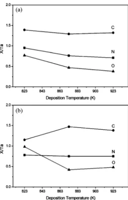
The quantities of Ta, C, N and O elements in the films were estimated from EPMA studies. Relatively high elemental contaminations are shown in Fig. 9. Using Ar as the carrier gas, the elemental ratio of C : Ta, 1.3–1.4, does not change much. The elemental ratios of N : Ta and O : Ta decrease from 1.0 to 0.7 and from 0.8 to 0.4, respectively, as the temperature of deposition is raised from 823 to 923 K. As mentioned above, the films deposited at low temperatures are more susceptible to oxidation by oxygen and moisture in the environment. The film deposited at 923 K showed the lowest sheet resistance value of ca. 1700 mV cm. This is higher than the reported values of
TaC28and TaN16films. The films grown at low temperatures showed significantly higher resistivity. Oxygen and graphitic carbon in the films probably caused the resistivity increase.
From the XRD data and the elemental composition studies above, differentiating whether the thin films are made of a homgeneous mixture of TaC and TaCN crystals, or of a single phase tantalum carbonitride solid, presents an ambiguity. Both cubic TaC23and TaN32crystallize in a NaCl structure. Their lattice constants, aTaC~ 0.4454 nm and aTaN~ 0.433 nm, are
close. This reflects the similar atomic sizes of C and N and their similar bonding behavior to Ta. The imido complex used as the precursor is so-called ‘single-source’, i.e. containing all the elements in the film in a single type of molecule. After the precursor is thermolyzed, the elements in the thin films probably are homogeneously mixed at the atomic level. At the low growth temperatures employed, separation of the elements into discrete TaC and TaN phases is difficult. A similar phenomenon has been observed for the growth of thin films from Ti(NEt2)4and related coplexes.13,15Thus, the
deposited material is more likely to be a cubic phase tantalum carbonitride, with the C and N atoms mixed in a structure resembling cubic TaC and TaN.
Volatile products formed in the reactions were collected and identified to be predominantly neopentane. Trace amounts of isobutylene and 2,2,5,5-tetramethylhexane were also detected. Nitrogen-containing compounds (excluding N2) were below
the detection limit, which indicates that the TaLN double bond did not undergo significant cleavage. Most of the nitrogen atoms are incorporated into the films in the form of nitride. It is difficult to differentiate whether the carbon atoms in the films were from the imido ligand or from the neopentyl ligand. Previous studies have shown that the tert-butyl groups of the tert-butylimido ligand liberated isobutylene through a c-hydrogen elimination process.16–18 We speculate that the source of the carbide atoms is more likely to be from the neopentyl ligands,4–12 generated via the pathways shown in Scheme 1 discussed above.
Fig. 8 High-resolution XPS spectra of the film on Si(100) grown at 923 K from Me3CNLTa(CH2CMe3)3in Ar: (a) Ta 4f5/2and Ta 4f7/2
electrons, (b) N 1s electrons, and (c) C 1s electrons.
Fig. 9 Estimated concentrations of Ta, C, N and O elements in the films on Si(100) deposited from Me3CNLTa(CH2CMe3)3, grown in
(a) Ar, and (b) H2.
J. Mater. Chem., 2003, 13, 365–369
Conclusion
It is proposed that these two precursors decomposed via similar pathways, involving a- and c-hydrogen activation of the ligands. Two novel Ta complexes, Me3CCHLTa(CH2CMe3)3
and Me3CNLTa(CH2CMe3)3, were employed as the precursors
to deposit TaC and TaCN thin films successfully by chemical vapor deposition. A generalized reaction pathway is shown in Scheme 2 to summarize this study. EPMA data of the TaC films showed that the elemental ratios of C : Ta varied from 0.5 to 1.6 as the deposition conditions changed. The elemental ratios of C : Ta and N : Ta in TaCN films varied from 1.1, 0.7 and to 1.5, 1.0, respectively. Possible reaction pathways were proposed according to the analysis of the volatile products. It is suggested that the alkylidene carbon atom of Me3CCHL
Ta(CH2CMe3)3 is incorporated into the films to form a
carbide. On the other hand, the nitrogen atom of Me3CNL
Ta(CH2CMe3)3becomes the nitride in the film.
Acknowledgement
The authors thank the National Science Council of Taiwan, Republic of China, for financial support (NSC-90-2113-M-009-022).
References
1 S. T. Oyama, The Chemistry of Transition Metal Carbides and Nitrides, Blackie Academic & Professional, Glasgow, 1996. 2 H. O. Pierson, Handbook of Refractor Carbides and Nitrides,
Noyes Publications, New Jersey, 1996.
3 S. N. Yoganand, M. S. Raghuveer, K. Jagannadham, L. Wu, A. Karoui and G. Rozgonyi, Appl. Phys. Lett., 2002, 80, 79. 4 G. S. Girolami, J. A. Jensen, D. M. Pollina, W. S. Williams,
A. E. Kalogeros and C. M. Allocca, J. Am. Chem. Soc., 1987, 109, 1579.
5 J. Cheon, D. M. Rogers and G. S. Girolami, J. Am. Chem. Soc., 1997, 119, 6804.
6 J. Cheon, L. H. Dubois and G. S. Girolami, J. Am. Chem. Soc., 1997, 119, 6814.
7 D. C. Smith, R. R. Rubiano, M. D. Healy and R. W. Springer, Mater. Res. Soc. Symp. Proc., 1993, 282, 643.
8 M. D. Healy, D. C. Smith, R. R. Rubiano, N. E. Elliott and R. W. Springer, Chem. Mater., 1994, 6, 448.
9 N. M. Rutherford, C. E. Larson and R. L. Jackson, Mater. Res. Soc. Symp. Proc., 1989, 131, 439.
10 F. Maury, F. Ossola and F. Schuster, Surf. Coat. Technol., 1992, 54, 204.
11 Z. Xue, K. G. Caulton and M. H. Chisholm, Chem. Mater., 1991, 3, 384.
12 Z. Xue, S.-H. Chuang, K. G. Caulton and M. H. Chisholm, Chem. Mater., 1998, 10, 2365.
13 H.-T. Chiu and C.-C. Huang, Mater. Lett., 1993, 16, 194. 14 K. Sugiyama, S. Pac, Y. Takahashi and S. Motojima,
J. Electrochem. Soc., 1975, 122, 1545.
15 R. M. Fix, R. G. Gordon and D. M. Hoffman, Chem. Mater., 1990, 2, 235.
16 M.-H. Tsai, S.-C. Sun, H.-T. Chiu, C.-E. Tsai and S.-H. Chuang, Appl. Phys. Lett., 1995, 67, 1128.
17 M.-H. Tsai, S.-C. Sun, H.-T. Chiu and S.-H. Chuang, Appl. Phys. Lett., 1996, 68, 1412.
18 E. L. Crane, H.-T. Chiu and R. G. Nuzzo, J. Phys. Chem. B, 2001, 105, 3549.
19 C. H. Winter, P. H. Sheridan, T. S. Lewkebandara, M. J. Heeg and J. W. Proscia, J. Am. Chem. Soc., 1992, 114, 1095.
20 R. R. Schrock and J. D. Fellmann, J. Am. Chem. Soc., 1978, 100, 3359.
21 P.-J. Chang, Master Thesis, National Chiao Tung University, Hsinchu, Taiwan, R. O. C., 2000.
22 H.-T. Chiu, S.-H. Chuang, C.-E. Tsai, G.-H. Lee and S.-M. Peng, Polyhedron, 1998, 17, 2187.
23 Powder diffraction file card 35-0801 (TaC), JCPDS, International Center for Diffraction Data, Swarthmore, PA, USA.
24 L. Ramqvist, K. Hamrin, G. Johansson, U. Gelius and C. Nordling, J. Phys. Chem. Solids, 1970, 31, 2669.
25 G. R. Gruzalski and D. M. Zehner, Phys. Rev. B, 1986, 34, 3841.
26 A. K. Dua and V. C. George, Thin Solid Films, 1994, 247, 34. 27 J. F. Moulder, W. F. Stickle, P. E. Sobol and K. D. Bomben,
Handbook of X-Ray Photoelectron Spectroscopy, Perkin-Elmer, Minnesota, 1992.
28 T. Jang, L. M. Porter, G. W. M. Rutsch and B. Odekirk, Appl. Phys. Lett., 1999, 75, 3956.
29 Comprehensive Organometallic Chemistry, E. W. Abel, F. G. A. Stone and G. Wilkinson, ed., Pergamon Press Ltd., Oxford, UK, 1982.
30 F. C. Whitmore, A. H. Porkin, H. I. Bernstein and J. P. Wilkins, J. Am. Chem. Soc., 1941, 63, 124.
31 K. H. Anderson and S. W. Benson, J. Chem. Phys., 1964, 40, 3747. 32 Powder diffraction file card 32-1283 (TaN), JCPDS, International
Center for Diffraction Data, Swarthmore, PA, USA.
33 K. Sasaki, A. Noya and T. Umezawa, Jpn. J. Appl. Phys., 1990, 29, 1043.
Scheme 2
J. Mater. Chem., 2003, 13, 365–369