國
立
交
通
大
學
光電工程學系顯示科技研究所
碩
士
論
文
可應用於折射率感測器的高 Q 值表面模態
二維光子晶體板緣共振腔之研究
Researches on High Quality Factor Surface
Mode in Two-Dimensional Photonic Crystal
Slab-Edge Microcavity for Index Sensing
研 究 生:蕭逸華
指導教授:李柏璁 教授
可應用於折射率感測器的高 Q 值表面模態
二維光子晶體板緣共振腔之研究
Researches on High Quality Factor Surface Mode in Two-Dimensional
Photonic Crystal Slab-Edge Microcavity for Index Sensing
研 究 生:蕭逸華 Student:Yi-Hua Hsiao
指導教授:李柏璁 教授 Advisor:Dr. Po-Tsung Lee
國立交通大學
光電工程學系 顯示科系研究所
碩士論文
A Thesis
Submitted to Department of Photonics and Display Institute College of Electrical Engineering and Computer Science
National Chiao Tung University In partial Fulfillment of the Requirements
for the Degree of Master In
Electro-Optical Engineering July 2009
Hsinchu, Taiwan, Republic of China
I
可應用於折射率感測器的高
Q
值表面模態
二維光子晶體板緣共振腔之研究
學生:蕭逸華
指導教授:李柏璁 教授
國立交通大學光電工程學系顯示科技研究所碩士班
摘
要
由於超小的模態體積,利用二維光子晶體共振腔應用於折射率感測器,可以比其 他光學方法所製作的感應器能偵測更小的範圍。為了獲得更高的感測度與最小的可偵 測折射係數,在本論文中我們首先討論典型的二維光子晶體板緣共振腔,這種板緣共 振腔最大特色就是將模態聚集在表面而容易達到高感測度,利用此特性並且藉由調變 不同的切面比例以及透過三維有限時域差分法,我們可以計算此共振腔的Q值與感測 度。為了更進一步最佳化Q值,我們設計了異質結構的板緣共振腔,利用其模態能隙 的原理,可以較平緩地將模態聚集在共振腔內,因此大幅提升了Q值,並且也降低了 其所對應最小的可偵測折射係數值。 接著用半導體製程方法將實際元件製作出來,並利用共焦顯微螢光光譜系統來量 測基本的雷射特性。此外並且架設氣體真空腔系統,透過注入純二氧化碳與改變不同 的氣壓,來調變此元件所處的環境折射係數,經由共焦顯微螢光光譜系統來觀察共振 波長的位移,以此來計算感測度與最小可偵測折射係數值,最後將量測結果討論與分 析。
II
Researches on High Quality Factor Surface
Mode in Two-Dimensional Photonic Crystal
Slab-Edge Microcavity for Index Sensing
Student:Yi-Hua Hsiao
Advisors:Prof. Po-Tsung Lee
Department of Photonics & Display Institute,
National Chiao Tung University
Abstract
The two-dimensional photonic crystal microcavity could be applied for refractive index sensing, which could detect the smaller region than another optical method due to the ultra-small mode volume. In order to obtain the higher sensitivity and smaller detectable resolution of refractive index, in this thesis, first we discuss typical two-dimensional slab-edge-mode microcavity. The merit of this type microcavity is the mode concentrating in the surface and easily to obtain high sensitivity. From this characteristic, we apply 3D finite-difference time-domain method to simulate the quality (Q) factor and sensitivity by varied different truncated facets. In order to further optimize the Q factor, we demonstrate hetero-slab-edge microcavities. The electric field is confined gently by mode-gap effect, therefore the Q factor is increasing suddenly, and the minimum detectable refractive index is also decreasing.
And we fabricate the real device by a series of fabrication processes. The basic lasing characters are measured by micro-PL system. In addition, we build a gas chamber to change the device environment refractive index by controlling the different pressure of carbon dioxide. The sensitivity and minimum detectable refractive index could be calculated by this experiment. Finally, we will discuss and analysis these results.
III
Acknowledgements
兩年的研究生涯很快就過去了,很感謝指導教授李柏璁老師兩年來的指教, 老師對於我在光子晶體領域的研究當中給予了我很大的幫助,使我受益匪淺。在 老師的主持下,實驗室的風格在實驗與課業上表現很認真,娛樂休閒時大家也會 一起快樂地去打球,讓我這兩年過的相當充實。 特別感謝實驗室大師兄盧贊文學長,在理論、模擬、實驗、量測各個方面給 的超級專業與權威性的建議,並且對於口頭報告的邏輯思維,以及投影片、論文 的製圖美學給我的超細膩與龜毛的要求和訓練,讓我這輩子受用無窮。在碩一什 麼都不太懂的時候,很感謝林孟穎學姐、施均融學長、蔡宜育學長在製程與模擬 上面的指導,讓我順利傳承了學長姐的經驗,快速上手製程機台。 也很感謝同組的戰友何韋德同學,除了在製程上面幫了很大的忙以外,在這 碩士班兩年當中從 OPT、CLEO、以及畢業論文和口試,每次都一起奮鬥與加班, 一次又一次地一起完成挑戰。感謝年紀比我大的學弟佐哥林品佐,也幫忙了我很 多的實驗,祝福你以後 Ebeam 能越寫越準而且越圓,承先啟後繼往開來。也感謝 學長張資岳、張明峰、王明璽、宋和璁、江俊德、蔡家揚及郭總郭光揚,學弟蕭 君源、張鈞隆、蔡宜恆、鄭又瑋,同學林怡先、李欣育、洪青樺,高中同學、大 學的好朋友、以及親愛的家人,感謝大家,因為你們讓我在碩士的兩年生涯不會 感覺孤單,可以圓滿成功地完成碩士學位。 最後再一次感謝親愛的家人一路地支持與鼓勵,感謝所有在這兩年我所見所 聞與影響我的人,謝謝所有幫忙我的人,因為這些我所感謝的人,才能交織成我 這輩子很難忘、快樂充實的兩年。 蕭逸華。2009 年 8 月 謹誌於 新竹交通大學交映樓IV
Content
Abstract (In Chinese)………..…….……….……….…………..……….I Abstract (In English) ……….………..……….….II Acknowledgements….…………..………..……..……….III Content………..………...……...…IV Figure Captions………...………...VI Table Caption………...……..……….………IX Chapter 1 Introduction ... 1 1.1 Optical Index Sensor ... 1 1.2 Surface Wave in Dielectric Photonic Crystal ... 3 1.3 Background and Motivation ... 5 1.4 Overview ... 8 Chapter 2 High Q Surface Wave in PhC Slab‐Edge Microcavity ... 9 2.1 Introduction ... 9 2.2 Surface Wave in PhC Slab Edge ... 10 2.2.1 Plane Wave Expansion Method ... 10 2.2.2 Analysis of Surface Wave in PhC Slab Edge by PWE Method ... 11 2.3 Typical Slab‐Edge‐Mode Microcavity ... 14 2.3.1 Finite‐Difference Time‐Domain Method ... 14 2.3.2 Analysis of Typical SLEM Microcavity by FDTD Method ... 16 2.4 Hetero‐Slab‐Edge (HSE) Microcavity ... 22 2.4.1 Photonic Crystal Hetero‐Structure ... 22 2.4.2 HSE Microcavity Formed by Two Different τ ... 24 2.4.3 HSE Microcavity Formed by Three Different τ ... 26 2.4.4 Gradual Barrier HSE Microcavity ... 28 2.5 Conclusion ... 32 Chapter 3 Fabrications, Measurements ... 33 3.1 Introduction ... 33 3.2 Measurement Setup ... 40 3.2.1 The micro‐PL system ... 40 3.2.2 Gas chamber setup ... 41 3.3 Measurement Results ... 43 3.3.1 Measurement Results from Typical SLEM Microcavity ... 43 3.3.2 Measurement Results from HSE Microcavity Formed by TwoV Different τ ... 44 3.3.3 Measurement Results from HSE Microcavity Formed by Three Different τ ... 45 3.3.4 Measurement Results from Gradual Barrier HSE ... 46 3.4 PhC HSE microcavity for Index Sensing. ... 48 3.5 Conclusion ... 51 Chapter 4 Conclusions and Future Work ... 52
VI
Figure Captions
Figure 1.1 Scheme of 2D truncated PhC slab surrounded by air and the confinement of slab‐edge ... 3 Figure 1.2 (a) PhC hetero‐structure microcavity with air slot. (b) Electric field intensity profile of this cavity. (Adopted from reference [7]) ... 6Figure 1.3 (a) The SEM image and (b) the mode profile of the point‐shifted nanocavity. (c) Device soaked in liquids whose refractive index ranged from 1.00 to 1.37. Obvious, there are wavelength shift when the refractive index changing. (Adopted from reference [8]) ... 6
Figure 2.1 Scheme of 2D truncated PhC slab surrounded by air and the definition of slab‐edge termination parameter τ. ... 11
Figure 2.2 The calculated dispersion curves of τ=0.2, 0.5, and 0.8. ... 12
Figure 2.3 The simulated normalized frequency of SLEM under different τ by PWE method. The corresponding mode profiles of τ=0.2, 0.5, and 0.8 are also shown in the right insets. ... 13 Figure 2.4 Yee cell grid of 3D FDTD method. ... 16 Figure 2.5The microcavity design and confinement based on SLEM. ... 16 Figure 2.6 The simulated mode profiles in electrical‐field of SLEM microcavity with τ= (a) 0.3 and (b) 0.8. We can observe more electrical‐field concentration in air when τ=0.8, which leads to higher index sensitivity. ... 17 Figure 2.7 The simulated Q factor of SLEM microcavity with different τ ... 18 Figure 2.8 The simulated normalized frequency variation of SLEM microcavity ... 19 Figure 2.9 The simulated Q factors of SLEM microcavity with different cavity ... 20 Figure 2.10 The simulated Q factors of SLEM microcavity with different cavity ... 21 Figure 2.11 (a) The schematic of W1 PhC waveguide with lattice constant a. (b) The calculated band structure of (a). The up arrow indicates the transmission region and the down arrow indicates gap region. (c) Double‐hetero structure formed by different lattice a1 (in region I) and a2 (in region II) (d) the band structure along the waveguide direction. Photons only exist in the region II by the mode gap. (Adopted from reference [29]) ... 23
Figure 2.12 The simulated mode profiles of (a) double‐hetero structure and (c) L3 microcavity. The cross section electric field intensity of (b) double‐hetero structure and (d) L3 microcavity. (Adopted from reference [29]) ... 24 Figure 2.13 The calculated dispersion curves of SLEM with τ=0.3 and 0.35. ... 25 Figure 2.14 Scheme of PhC HSE microcavity formed by two different facets τ1 and τ2. L1 denotes cavity length. ... 26 Figure 2.15 (a) The simulated Q factor and mode volume versus L1. (b) The simulated
VII Q factor versus Δτ. ... 26 Figure 2.16 Scheme of PhC HSE microcavity formed by three different facets τ1 ,τ2 and τ3. L1 and L2 denote the cavity length and the barrier length, respectively. ... 27 Figure 2.17 The simulated Q factor and mode volume versus parameters (a) L2, (b) Δτ. ... 27 Figure 2.18 The simulated surface mode profiles in electrical field. ... 28 Figure 2.19 (a) Scheme of HSE interface formed by different slab‐edges F1 and F2. (b) The calculated dispersion curves of F1 and F2. ... 29
Figure 2.20 Scheme of PhC HSE microcavity. The gradual PhC barrier is formed by
gradually shrinking and shifting air holes at the slab edge. ... 30
Figure 2.21 The simulated Q factor and mode volume versus parameters (a) B and (b)
Δr/a. ... 31
Figure 2.22 The simulated surface mode profile in electrical field when L=10a, B=5,
and Δr/a=0.04 ... 31
Figure 3.1 A illustration of epitaxial structure of InGaAsP quantum wells for
membrane PhC lasers. The thickness of active region is about 220nm. . 34
Figure 3.2 The fabrication processes of two‐dimensional PhC membrane structure. 36 Figure 3.3 (a) Top‐view, (b) zoom‐in‐, and (c) tilted‐view SEM pictures of fabricated
typical SLEM microcavity with τ~0.34 ... 37
Figure 3.4 The SEM pictures of 2D PhC HSE microcavity formed by two different τ,
including (a) top‐view, (b) zoom‐in top‐view of fabricated, and (c) zoom‐in tilted‐view of fabricated slab edge. ... 38 Figure 3.5 The SEM pictures of 2D PhC HSE microcavity formed by three different τ, including (a) top‐view, (b) zoom‐in top‐view of fabricated, and (c) zoom‐in tilted‐view of fabricated slab edge. ... 38 Figure 3.6 SEM pictures of fabricated PhC gradual barrier HSE microcavity, including (a) tilted‐view, (b) top‐view of fabricated device, and zoom‐in tilted‐view of fabricated (c) slab edge and (d) PhC ... 39 Figure 3.7 The configuration of micro‐PL system ... 40 Figure 3.8 The illustration of the gas chamber system. ... 41 Figure 3.9 The typical (a) L‐L curve and (b) lasing spectrum of SLEM microcavity. Its threshold and SMSR can be estimated as 2.5mW and larger than 33dB. . 43 Figure 3.10 (a) The SLEM wavelength tuning by varying the lattice constant from 520
to 550 nm. (b) The measured polarization with polarized ratio ~6 from SLEM. ... 44
Figure 3.11 (a) The L‐L curve of HSE microcavity formed by two different τ and the
VIII at λ=1538. ... 45 Figure 3.12 (a) The L‐L curve of HSE microcavity formed by three different τ and the spectrum near threshold with Lorentzian fitting. (b) The lasing spectrum at λ=1528. ... 46 Figure 3.13 L‐L curves and spectrum near threshold with Lorentzian fitting... 46 Figure 3.14 (a) Lasing spectrum (curve A) near 1550 nm when pumping the cavity
region (position A), and spectra (curves B,C, and D) when pumping outside the cavity region (positions B, C, D). (b) The measured polarization with polarized ratio of 8. (c) The pumping position. ... 47
Figure 3.15 (a) The HSE microcavity formed by three different truncated facets
measurement results of resonance peak shift when the refractive index varied . The blue line indicates linear fitting. (b) The lasing spectra in the pressure 1 (1.24 atm) and pressure 2 (0.75 atm) conditions with Lorentzian fitting. ... 49
Figure 3.16 (a) The gradual barrier HSE microcavity formed by shrinking and shifting
air holes measurement results of wavelength shift in different environment index. (b) The lasing spectra of the pressure 1 (=1.13 atm) and pressure 2 (= 0.1 atm) with Lorentzian fitting. ... 49
IX
Table Caption
Table 2.1 The simulated index sensitivities and Q factor of SLEM microcavity with different τ………..181
Chapter 1 Introduction
1.1 Optical Index Sensor
During the last two decades there is an increasing need for sensitive optical sensors in areas such as environmental control, biotechnology, chemical engineering, etc., for the measurement of chemical and biological properties. For these applications, sensors should be compact, cheap, portage, and highly sensitive. Since then a great quantity of optical methods have been developed in chemical sensors and biosensors, mainly including interferometry [1], surface plasmon resonance [2], and recently photonic crystal microcavities also have been studied extensively for sensing [3-9].
Among them, the surface plasmon resonance due to the field concentration at the surface of material, ultrahigh sensitivities in various designs have been proposed and demonstrated [10]. It has been widely applied in demonstrating various optical sensors for chemical and biological applications, for example, drug discovery, gas compositions detecting, label-free biosensing, and so on. The surface plasma wave is a charge-density oscillation that could exist at the interface of two different material. The electromagnetic wave at the interface would satisfy the following expression [2]:
0
(1.1) where kz1, kz2 denote the free space wave vectors and ε1, ε2 the dielectric constants ofthe materials on the both sides, respectively. Therefore, one should be a minus number between ε1 and ε2 to satisfy equation (1.1). In the natural world, only the dielectric
constant of metal is minus in visible light wavelength, so only on the surface of metal may be excited surface plasmons. Due to the field concentration at the surface of
2
material, the surface plasmon resonance provides extremely high sensitivities of detectable refractive index in the range of 10-7~10-8 with detector areas of the order of 1mm2.
3
1.2 Surface Wave in Dielectric Photonic Crystal
In general, the surface plasma wave does not exist at the interface between dielectric materials. In 1966, the surface waves exist at the interface between a periodic dielectric layer and a homogeneous material that have been researched by Kossel [11]. The material with periodic index arrangement is the concept of photonic crystal (PhC) which has been proposed by E. Yablonovitch in 1987 [12]. A surface wave is defined as a propagating mode located near the interface between two material systems. The electromagnetic surface waves would propagate along the interface between the periodic structure of PhCs and air due to the photonic band gap (PBG) effect and total-internal-reflection (TIR) effect respectively. A typical 2D truncated PhC slab surrounded by air is shown in Fig. 1.1.
Figure 1.1 Scheme of 2D truncated PhC slab surrounded by air and the confinement of slab-edge
Lots of interesting designs of microcavity [13-16] and waveguide [17-26] based on surface wave in 2D PhCs have been reported and which are expected as important components in constructing versatile photonic integrated circuits (PhICs). Z. Zhang et al. have proposed an optical filter based on side coupling between silicon wire
4
waveguide and 2D PhC surface mode cavity [16]. H. Chen et al. have demonstrated a bi-directional coupler by using a conventional dielectric waveguide side coupled to the multimode surface modes in 2D PhC waveguide [17]. E. Moreno et al. have studied the surface mode collimated emission by appropriate corrugation of the PhC interface [18]. And J. K. Yang et al. have proposed slab-edge mode microcavities in 2D PhCs by designing various PhC mirrors in truncated PhC slabs, microcavities with confined surface waves can be formed [13].
Among above designs, the optical microcavities attract lots of attentions due to the abilities of well-confining photon flow locally in a condensed size and can be easily fused with other components by side-coupling ridge waveguides [16] in PhICs, which have been initiatively demonstrated and discussed recently.
5
1.3 Background and Motivation
In general, the resonant wavelength shifts as the environmental refractive index varies. Conversely, the refractive index could be detected by measuring the wavelength shift. We can define the environmental index sensing response value Rn as
Δλ/Δn [nm/RIU (refractive index unit)]. The detectable index variation can be obtained by inserting Rn and Q into following expression:
∆n
(1.2) where λ and λ/Q denote the wavelength and optical spectral linewidth, respectively.
Very recently, high sensitivity and condensed index sensors based on PhC defect micro- and nanocavities have been demonstrated and optimized theoretically, which show the abilities of sensing very small index variation in very condensed size. The surface plasmon resonance provides extremely high sensitivities in the range Δndet=10−7–10−8 but with detector areas of the order of 1mm2. By contrast, PhC
nanocavity sensors tend to have lower sensitivities Δndet =10−2–10−4 but can be
designed to fully localize the optical field to an area of 1 μm2, which can be readily integrated onto a chip.
S. H. Kwon et al. have proposed a PhC hetero-structure microcavity [7] with high index sensitivity of 512 nm / RIU in simulations as shown in Fig. 1.2. In this structure, double-hetero-structure with central holes has been designed to improve Q factor as high as 3.8×10⁶, and the corresponding Δndet is as small as 2.37×10⁻⁶. Beside,
the air slot is designed in the waveguide center which would extend the field into air to improve sensitivity, thus the Rn value could approach 512 in simulation.
6
Figure 1.2 (a) PhC hetero-structure microcavity with air slot. (b) Electric field intensity profile of this cavity. (Adopted from reference [7])
And S. Kita et al. [8] also demonstrate high index sensitivity device by point-shifted nanocavity with ultra-small mode volume in experiment as shown in Fig. 1.3. They soaked device in liquids whose refractive index ranged from 1.00 to 1.37, and obtained the maximum sensitivity of 350 nm/RIU and Δndet of 9.0×10⁻⁵
Figure 1.3 (a) The SEM image and (b) the mode profile of the point-shifted
nanocavity. (c) Device soaked in liquids whose refractive index ranged from 1.00 to 1.37. Obvious, there are wavelength shift when the refractive index changing. (Adopted from reference [8])
In these reports, in order to increase the environmental index sensing response (Rn), the defect mode fields are extended into environmental material (air) by
modifying cavity geometries. To further increase Rn, intuitively, the PhC microcavity
7
extends into environmental material, which is similar to the advantage of the high sensitivity surface plasmon resonance, and it has not been addressed and discussed in literatures. Besides, in addition to high Rn value, high quality (Q) factor mode is also
needed to provide fine optical spectral resolution and leads to high index sensitivity.
Thus, in this thesis, we propose, fabricate, and characterize a PhC slab-edge microcavity design, including typical slab-edge-mode (SLEM) microcavity, hetero-slab-edge microcavities formed by two and three different truncated facets, and gradual barrier hetero-slab-edge microcavity. The Q factor of surface mode is optimized in simulations by fine tuning the PhC patterns of the microcavity, which is aimed at achieving a high sensitivity optical index sensor.
8
1.4 Overview
In this thesis, in chapter 2, we will use finite-difference time-domain (FDTD) method and plane wave expansion (PWE) method to demonstrate the Q factor and sensitivity as environment index changing with different type and different truncated facet of surface mode microcavity. In chapter 3, the fabrication process of slab-edge mode photonic crystal microcavity structure will be illustrated. The measurement setup of micro-photoluminescence (micro-PL) system, the gas chamber setup for index sensing application, and measurement results will also be illustrated in chapter 3. And finally, we will take a brief conclusion in chapter 4.
9
Chapter 2 High Q Surface Wave in PhC Slab-Edge
Microcavity
2.1 Introduction
In this chapter, we focus our researches on Q factors and Rn values simulation of
PhC slab-edge mode (SLEM) microcavity. At first, the fundamental properties of the surface wave propagating in PhC slab edge will be calculated by the plan-wave-expansion (PWE) method. Then, the cavity will be designed in the slab edge by adding air holes in the two sides. The Q factors and Rn values will be
simulated by 3D finite-difference time-domain method (FDTD). In order to obtain the minimum detectable refractive index (Δndet) for sensing application, not only high
sensitivities but also high Q factors are necessary. Thus, we design hetero-slab-edge (HSE) mode microcavity to obtain high Q factors. The simulated results and discussions will be shown in this chapter.
10
2.2 Surface Wave in PhC Slab Edge
2.2.1 Plane Wave Expansion Method
Plane wave expansion (PWE) is a useful method to calculate the band-diagram in PhC. This method is similar to the way to deal with the behavior of an electron (Krong-Penny Model) in the periodic potential in solid-state physics. Therefore, in PhC, periodic dielectric distribution can also be expanded by reciprocal lattice vector ( ) in equation (2.1) and the wave function of photon in periodic dielectric distribution can also be expanded by the plane waves which are belong to the complete set of wave equation (2.2).
Periodic dielectric distribution: ε r ∑ UGeG·R
G (2.1)
Wave function of Photon: ψ r ∑ M k G e G ·R
G (2.2)
Wave equation: E r E r (2.3) Finally, we substitute the equation (2.1) and (2.2) into the wave equation (2.3) in source free region from Maxwell equation, we will get new wave equation:.
k G · k G EG ω ∑ εG G,G EG (2.4) This equation can be expressed as matrix form and the dispersion curve can be solved. The wavevector k is arbitrary, but can be replaced by k in the first Brillouin zone which is due to the translational symmetry inhered in PhC. Hence, we can limit our calculation in the first Brillouin zone. The εG,G is the Fourier coefficient of ε(r) and ε-1(r), which is concerning to G-G’. In this thesis, all the band diagrams of PhC would be calculated by this method.
11
2.2.2 Analysis of Surface Wave in PhC Slab Edge by PWE
Method
Surface waves are propagating electromagnetic waves which are optically confined both by TIR and PBG effects at the surface of a PhC slab. The scheme of a typical 2D truncated PhC slab surrounded by air is shown in Fig. 2.1. The propagating frequency would be varied when we design different truncated facets of the air holes at the surface of the PhC slab. The PhC slab termination parameter τ (from 0 to 1) is defined as in Fig.2.1.
Figure 2.1 Scheme of 2D truncated PhC slab surrounded by air and the definition of slab-edge termination parameter τ.
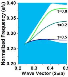
In order to realize the properties of SLEM, at first, the PWE method is applied to calculate the dispersion curves in Fig. 2.2. The dielectric slab thickness and refractive index are 220nm and 3.4. The lattice constant (a) and air-hole radius (r) over a (r/a) ratio are set to be 520nm and 0.37. This figure shows the dispersion characteristics of the SLEM, the dispersion curves of the SLEMs are found in the PBG region for wide range of τ. As the wavevector near to the band edge, the slope of the dispersion curve would decrease to signify that the group velocity of the mode decreases. Therefore the SLEM near to the band edge is suitable for lasing. The normalize frequencies of the
12
PhC SLEM at the band edge are plotted with different terminations τ in Fig. 2.3, and also shows the corresponding mode profiles of τ=0.2, 0.5, and 0.8. The magnetic fields of the SLEM are strongly confined to near the truncated slab-edge. In general, the lower normalize frequency would lead to the higher mode concentration in the high dielectric region. Therefore the frequency of SLEM decreases when τ increases, which is due to the increased electromagnetic field concentration in the high dielectric region. In Fig. 2.3, we could anticipate that if we design SLEM microcavity structure, the highest Q factor will be found in τ=0.2~0.3, which is due to the frequency in the mid-gap. We also could anticipate the highest Rn value would be found in τ=0.6~0.8,
because the high frequencies are near the air band that would increase electromagnetic field concentration in the low dielectric region
13
Figure 2.3 The simulated normalized frequency of SLEM under different τ by
PWE method. The corresponding mode profiles of τ=0.2, 0.5, and 0.8 are also shown in the right insets.
14
2.3 Typical Slab-Edge-Mode Microcavity
2.3.1 Finite-Difference Time-Domain Method
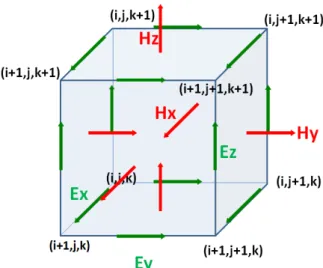
To simulate the behavior of electromagnetic wave in PhC, the Finite-Difference Time-Domain (FDTD) method is used most often. The FDTD method is applied to directly solve the Maxwell equation.
Maxwell equations are vector differential equations, but computers can only operate scalar add or subtract. Therefore, the Maxwell equations should be transformed into six scalar differential equations. FDTD method is developed to compute these six equations discretely. These six scalar differential equations for each field component of Faraday’s law and Ampere’s law are given by equation (2.6), where s and σ denote the magnetic loss and conductivity.
∂E ∂z ∂E ∂y s µ µ ∂ ∂t H ∂E ∂x ∂E ∂z s µ µ ∂ ∂t H ∂E ∂y ∂E ∂x s µ µ ∂ ∂t H ∂H ∂y ∂H ∂z σ ε ε ∂ ∂t E ∂H ∂z ∂H ∂x σ ε ε ∂ ∂t E ∂H ∂x ∂H ∂y σ ε ε ∂ ∂t E (2.6) For PhC simulation, the refractive index distribution is not uniform and may be dependent on the positions. Hence, in order to describe the distribution of the
15
refractive index, all spaces are divided into many grids. The widely used grid form adopted in the FDTD is Yee cell as shown in Fig. 2.4. The index i, j, k denote the positions of grid points in Cartesian coordinates. The magnetic fields are centered on the facet, and the electric fields are arranged on the edges of the cubic, which is due to the electric fields updated are induced midway during each time step between successive magnetic fields, and conversely. Therefore, the electric and magnetic functions could be express as F(iΔx, jΔx, kΔx, nΔt)=Fn(xi, xj, xk) at the nth time
step, where Δx is the increment of length and Δt is the increment of time step. The
six differential equations could discrete into the form as equation (2.7), and the six field components E / , E / , E / , H / , H / , H / at the n+1/2 time step can be expressed with the field at the nth time step. The detail mathematical
expression can be found in reference [27]. Later, we will use this FDTD method to realize the properties of our microcavity design.
∂F x , x , x ∂x F x / , x , x F x / , x , x Δx ∂F x , x , x ∂x F x , x / , x F x , x , x / Δx ∂F x , x , x ∂x F x , x , x / F x , x , x / Δx ∂F x , x , x ∂t F / x , x , x F / x , x , x Δt (2.7)
16
Figure 2.4 Yee cell grid of 3D FDTD method.
2.3.2 Analysis of Typical SLEM Microcavity by FDTD Method
Based on the SLEM which we has discussed in Chapter 2.2, we design a microcavity by PhC slab-edge with air holes in the right-side and left-side as shown in Fig 2.5. The SLEM will be confined between the two-side air holes by PBG effect. We apply 3D FDTD simulation to investigate the SLEM in this microcavity. The lattice constant, r/a ratio, cavity length, and τ are set to be 520 nm, 0.37, 5.1 μm, and 0.2 to 0.8, respectively.
17
The simulated mode profiles of SLEM with τ= 0.3 and 0.8 are shown in Fig. 2.6. The right figure is the field intensity with different position along the red line in the left figure. In the right figure, the field intensity would decay in the left side of the slab-edge by TIR effect and decay in the right side of the slab-edge by PBG effect. We could observe that the field as τ=0.8 is much concentrative in air region than τ=0.3, which is the same as our discussion in Chapter 2.2.2.
Figure 2.6 The simulated mode profiles in electrical-field of SLEM microcavity
with τ= (a) 0.3 and (b) 0.8. We can observe more electrical-field concentration in air when τ=0.8, which leads to high index sensitivity.
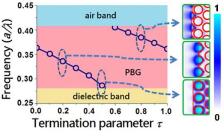
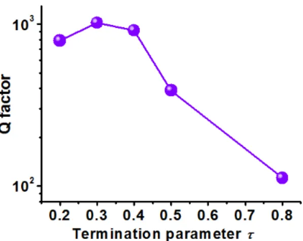
Then, we calculate the Q factor of SLEM with different τ and find the highest and lowest Q factors of 1,021 and 112 when τ =0.3 and 0.8, as shown in Fig. 2.7. The former and latter values are attributed to the SLEM frequencies that lie in mid-gap and edge of the PBG, respectively, as shown in Fig 2.3.
18
Figure 2.7 The simulated Q factor of SLEM microcavity with different τ
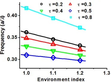
We also calculate the SLEM modal frequency variation of microcavities with different τ by varying the environmental index from 1.0 to 1.2, as shown in Fig. 2.8. We obtain index sensitivity as high as 744 nm / RIU ever reported when τ = 0.8. This high sensitivity can be attributed to the more electrical-field concentration in the low-dielectric region as shown in the field profile in Fig. 2.6 (b). However, when considering the low Q factor of 112, the minimum detectable index variation (Δndet) is
only 0.015. On the other hand, for higher Q factor of 1,021 in SLEM microcavity with
τ = 0.3, the index sensitivity is 610 nm / RIU. This high value is also attributed to the
similar phenomenon with τ = 0.8. The Δndet is then estimated to be 2.39×10⁻³, which is
much better than the case when τ = 0.8. The calculated results of other conditions are listed in Table 2.1. In Table 2.1, the index sensitivity decreases when τ is varied from 0.2 to 0.5, which is mainly attributed to the less electrical-field concentration in the low-dielectric region.
19
Figure 2.8 The simulated normalized frequency variation of SLEM microcavity
with different τ when the environmental index is varied from 1.0 to 1.2
τ Q Factor Sensitivity (nm/RIU) Δndet
0.2 794 656 2.76 × 10⁻³
0.3 1021 610 2.39 × 10⁻³
0.4 916 520 3.30 × 10⁻³
0.5 390 344 1.25 × 10⁻²
0.8 112 744 1.50 × 10⁻²
Table 2.1 The simulated index sensitivities and Q factor of SLEM microcavity with different τ.
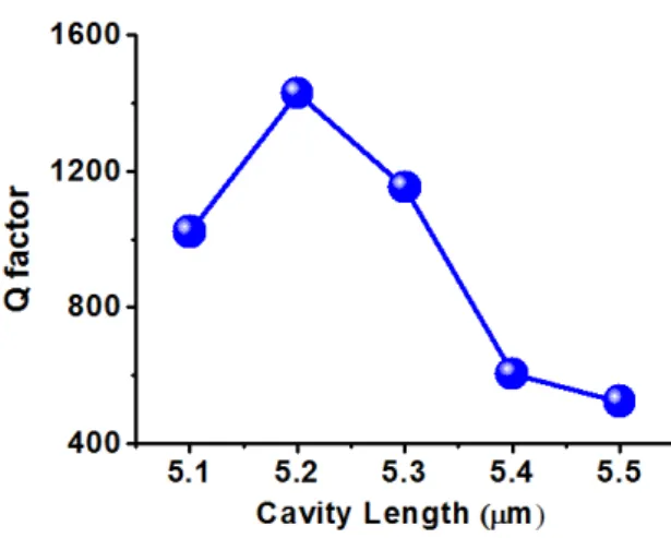
From the results in Table 2.1, we can conclude that high index sensing resolution requires both high index sensitivity and Q factor of microcavity. Thus, in order to improve the Q factor of SLEM microcavity with τ = 0.3, the cavity length defined in Fig. 2.5 is varied from 5.1 to 5.5 μm. From the simulated results in Fig. 2.9, we obtain high simulated Q factor of 1,429 when the cavity length is 5.2 μm, which just equals to ten times to lattice constant. The index sensitivity then becomes 609 nm/RIU and
20
the Δndet is estimated to be 1.71×10⁻³. Although this value is still not small enough, the
Q factor can be further optimized carefully and lead to improved Δndet.
Figure 2.9 The simulated Q factors of SLEM microcavity with different cavity
length.
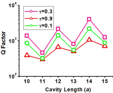
Beside, the Q factor of the SLEM as a function of cavity length from 10a to 15a is shown in Fig. 2.10. The SLEM could go through the cavity region but reflect by the right-side and left-side PhC air holes. As described in Ref. [28], for observing Fabry-Perot condition, Q factor might be enhance when the round-trip accumulated phase Ф=2kL+2Δφ is a multiple of 2π, where L denotes cavity length and Δφ denotes the phase shift from the boundary reflection. Our left-side and right-side PhC air holes are strong reflectors which could let Δφ close to π. In Fig. 2.2, our nearly zero group velocity could be found for the wave vector k=0.5 (2π/a). Hence, the round-trip accumulated phase Ф is reduced to (L/a)π+2π. Therefore, the Q factor would be enhanced when cavity length is a multiple of 2a. As the cavity length increases, the Q factors will fluctuate but in average increasing which is due to the photon life time also increasing.
21
Figure 2.10 The simulated Q factors of SLEM microcavity with different cavity
lengths from 10a to 15a when τ = 0.3, 0.9,and 0.1.
Actually, the Q factor can be increased up to larger than 10,000 by simply enlarging the cavity length to be 20a. And the Δndet will become as small as 2×10⁻⁴.
However, considering the compact device size requirement, other approaches such as gradual interface designs will be better than enlarging the microcavity in our device which will be discussed in Chapter 2.4.
22
2.4 Hetero-Slab-Edge (HSE) Microcavity
2.4.1 Photonic Crystal Hetero-Structure
Over the past decades, hetero-structure has been widely used in semiconductor. In semiconductor, hetero-structure can be formed by using different band-gap materials and strains. The PhC also can be formed hetero-structure by tuning some parameters in different region. Generally, the hetero-structure can be created by simply tuning the size of air holes, the position of the air holes, the lattice constant , or anything which could change the normalize frequency slightly.
B.S. Song has proposed ultra-high-Q photonic double-hetero structure nanocavity as shown in Fig. 2.11 [29]. First, the waveguide mode has been simulated in a 2D PhC slab of triangular-lattice structure with a line defect waveguide formed by a missing row of air holes (W1 waveguide) as shown in Fig. 2.11 (a). The up arrow indicates the transmission region, and the down arrow indicates the mode-gap region. Then, the hetero-structures created by connecting two PhC structures I and II with different lattice constants a1 and a2. We could observe the band diagram along the
waveguide direction in Fig.2.11 (d), photons can exist only in the PhC II region by mode-gap confinement. Follow this mod-gap confinement principle, Q factors greater than 2×10⁷ may be obtained theoretically when optimizing the structure. Later, we will improve Q factor of our SLEM microcavity by this mod-gap effect.
23
Figure 2.11 (a) The schematic of W1 PhC waveguide with lattice constant a. (b)
The calculated band structure of (a). The up arrow indicates the transmission region and the down arrow indicates gap region. (c) Double-hetero structure formed by different lattice a1 (in region I) and a2 (in region II) (d) the band
structure along the waveguide direction. Photons only exist in the region II by the mode gap. (Adopted from reference [29])
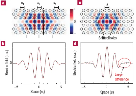
The mode profile of this double-hetero structure in Fig. 2.12 (a) could be compared to triangular-lattice structure with three air holes missing and boundary modulated slightly microcavity (L3 micocavity) in Fig 2.12 (c). The cross section field intensity is shown in Fig. 2.12 (b) and (d). Obviously, the double-hetero structure is confined gently, and the cross section field intensity is much similar to Gaussian function which leads high Q factor but lager mode volume. On the contrary, the L3 microcavity is confined sharply, and the field has a large difference with Gaussian function in the cavity boundary. Therefore the Q factor is less but mode volume is smaller than the double-hetero structure.
24
Figure 2.12 The simulated mode profiles of (a) double-hetero structure and (c)
L3 microcavity. The cross section electric field intensity of (b) double-hetero structure and (d) L3 microcavity. (Adopted from reference [29])
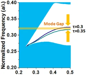
2.4.2 HSE Microcavity Formed by Two Different τ
As described in Chapter 2.4.1, Q factors can be improved by hetero-structure. Here, we design the hetero-structure by different truncated facets. The dispersion curves of τ =0.3 and 0.35 are simulated by PWE method as shown in Fig. 2.13. There is a slight frequency shift between the bands of τ =0.3 and 0.35 and form the mode-gap. The light at slab-edge with τ =0.3 that lies inside the mode-gap region will regard the slab-edge with τ =0.35 as reflector.
25
Figure 2.13 The calculated dispersion curves of SLEM with τ=0.3 and 0.35.
The cavity design of PhC hetero-slab-edge (HSE) microcavity formed by two different τ is illustrated in Fig. 2.14. We denote the cavity length L1, the termination
parameter of cavity region τ1, and the termination parameter of barrier region τ2. The
3D FDTD method has been applied to simulate Q factors. The lattice constant a, r/a ratio are set to be 520 nm, 0.33, respectively. First, we fix τ1=0.2aand τ2=0.4a, and
tune different L1 from 2a to 10a to realize the relationship of Q factor and mode
volume versus L1, and which is shown in Fig 2.15 (a). The Q factor increases when
the cavity length increases which is due to increasing the photon life time. But the mode volume also increases linearly as cavity length increasing. We choose L1=10a
and further optimize Q factor by tuning the τ difference (τ2-τ1, Δτ) as shown in Fig.
2.15 (b). The Q factor increases when the τ difference decreases from 0.1 to 0.05. This result indicates that Q factors would be improve by gentler confinement. The τ difference decreases from 0.05 to 0.01 which will lead Q factors decrease, because the
τ difference is smaller than the simulated resolution, and just like a SLEM waveguide
that would not confine light. Finally, we obtain the highest Q factor about 1.8×10⁴ as τ2-τ1 =0.05.
26
Figure 2.14 Scheme of PhC HSE microcavity formed by two different facets τ1
and τ2. L1 denotes cavity length.
Figure 2.15 (a) The simulated Q factor and mode volume versus L1. (b) The
simulated Q factor versus Δτ.
2.4.3 HSE Microcavity Formed by Three Different τ
We further optimize Q factor with two barriers as shown in Fig. 2.16. For the same reason in Chapter 2.4.2, light wave will confine in the cavity region by the mode-gap effect. We denote the cavity length L1, the termination parameter of cavity
region τ1, the barrier length L2, the termination parameters of barrier regions τ2 and τ3
as shown in Fig. 2.16. The lattice constant a, r/a ratio are set to be 520 nm, 0.33, respectively. First, we fix L1=10a, τ1=0.3, τ2=0.35, τ3=0.4, and the Q factors are
27
simulated as a function of L2 by 3D FDTD in Fig. 2.17 (a). We tune L2 from 0a to 7a
and the highest Q Factor of 2.2×10⁵ is obtained when L2 = 2a. If L2 is larger or smaller
than 2a, this structure is just like to have only one barrier which we have discussed in Chapter 2.4.2. Therefore Q factors and mode volume would decrease as L2 is larger or
smaller than 2a. Now, L2 is fixed to 2a and the τ difference (Δτ=τ3-τ2=τ2-τ1) is tuned
from 0.01 to 0.1 in Fig. 2.17 (b). We obtain high Q factor of 5.4×10⁵ , large Rn factor
of 591 nm/RIU, and ultra-small Δndet of 4.7×10⁻⁶, when τ1=0.3, τ2=0.34, τ3=0.38,
which is very potential in achieving highly sensitive optical index sensor. The simulated mode profile in electrical field is shown in Fig. 2.18.
Figure 2.16 Scheme of PhC HSE microcavity formed by three different facets
τ1 ,τ2 and τ3. L1 and L2 denote the cavity length and the barrier length, respectively.
Figure 2.17 The simulated Q factor and mode volume versus parameters (a) L2,
28
Figure 2.18 The simulated surface mode profiles in electrical field.
2.4.4 Gradual Barrier HSE Microcavity
To form the hetero-structure, not only different truncated facets but shrunk or shifted air holes could achieve. Here we design a barrier region by shrinking and shifting the air holes at the slab edge, which is shown and denoted as F2 in Fig. 2.19
(a). When the air holes are modified as described above, the surface mode frequency will become lower as shown in Fig. 2.19 (b). For a 2D truncated PhC HSE interface formed by slab-edges F1 and F2 shown in Fig. 2.19 (a), the surface mode with
frequency inside the range indicated in Fig. 2.19 (b) will propagate in slab-edge F1
and regards the slab-edge F2 as a mirror, which forms the mode-gap effect. Thus, we
can design a microcavity by applying double HSE interfaces as shown in Fig. 2.20.
In our PhC HSE microcavity design, the r/a ratios of PhC lattice [white circles in Fig. 2.20] and microcavity region (red circles) are the same (fixed r and a) and set to be 0.36 initially. The microcavity length L, and slab thickness are set to be 10a and 220 nm, respectively. The barrier region with mode-gap effect is designed by
29
Figure 2.19 (a) Scheme of HSE interface formed by different slab-edges F1 and
F2. (b) The calculated dispersion curves of F1 and F2.
shrinking and shifting the air holes at the slab edge, as illustrated in Fig. 2.20. To obtain high Q microcavity, the air holes of the barrier region are shrunk and shifted gradually, from orange (number 1) to purple (number 5) circles shown in Fig. 2.20. The number of periods of the gradual barrier region is denoted as B. This gradual barrier design is mainly expected for gentle mode-gap confinement and the reduction of optical scattering losses in the barrier region. The r/a ratios of the remaining outer barrier region with purple circles in Fig. 2.20 are kept the same, and the r/a ratio difference between microcavity and outer barrier is denoted as Δr/a. Thus, the r/a difference between air holes in the gradual barrier region is Δr/a ×1/B.
30
Figure 2.20 Scheme of PhC HSE microcavity. The gradual PhC barrier is
formed by gradually shrinking and shifting air holes at the slab edge.
To optimize the Q factor of PhC HSE microcavity, we vary the parameter B from 0 to 5 with Δr/a=0.03. The simulated Q factor and effective mode volume V by 3D FDTD simulations are shown in Fig. 2.21 (a). When B=0 (no gradual barrier), the low
Q factor of 2.8×10⁴ is mainly attributed to the scattering losses of the HSE interface with sharp r/a ratio variation between barrier and microcavity. Once the gradual barrier periods increase, the gentle confinement due to gentle r/a ratio variation will be provided, which leads to the increased Q factor. When B=5, the Q factor increases to 2×10⁵. Besides, the mode volume also increases monotonically with B. This indicates the mode profile extends more into the gradual barrier region, which is caused by the gentler mode confinement. Then we further optimize the Q factor by varying Δr/a from 0.01 to 0.1 when B=5. The simulated results are shown in Fig. 2.21 (b). When Δr/a is small, the mode-gap confinement is weak and the mode will extend into the barrier, which leads to low Q factor and large mode volume. On the other hand, when Δr/a becomes too large, extra scattering losses are induced due to sharp mode confinement. Therefore, the Q factor is decreased and less mode profile extends into the gradual barrier region, which leads to small mode volume. Thus, we obtain an optimized high Q factor of 6.6×10⁵ when Δr/a =0.04 with V of 2.25×(λ/n)3. The simulated surface mode profile in electrical field is shown in Fig. 2.22. From Fig. 2.22, one can observe the significant electrical field concentrations in the air region, which implies high sensitivity of this surface mode to the environmental index variation. To address the potential of our PhC HSE microcavity serving as a high-sensitivity index sensor, we calculated the Rn value by setting the environmental
31
microcavity design with Q factor of 6.6×10⁵ in Fig. 2.21 is applied. The calculated wavelength variation of 12.5 nm when the environmental index varied from 1 to 1.02, which corresponds to a large Rn value of 625 nm/RIU. The calculated Δndet is as small
as 3.6×10⁻⁶. This small value actually can be further decreased by optimizing the parameter τ and r/a ratio of PhC HSE microcavity for higher Rn and Q factor. We
believe the very small Δndet close to that of conventional interferometer can be
expected and achieved by this PhC microcavity design, which is with very condensed device size.
Figure 2.21 The simulated Q factor and mode volume versus parameters (a) B
and (b) Δr/a.
Figure 2.22 The simulated surface mode profile in electrical field when L=10a,
32
2.5 Conclusion
In this chapter, in order to achieve highly sensitivity optical index sensor, we design and simulate SLEM microcavity. The mode profile in electrical field of SLEM would extend to environment which is advantageous for index sensing. Therefore, we propose typical SLEM micrcavity by adding air holes in the left-side and right-side of SLEM waveguide. We calculate the Q factor and Rn value of SLEM microcavity with
different τ. Highest Q factor and Rn value of 1,021 and 744 nm/RIU are obtained
when τ=0.3 and 0.8, respectively. When considering the minimum Δndet is 2.4×10⁻³ as
τ=0.3, which is obviously limited by the law Q factor.
To further increase the Q factor, the hetero-structure with mode-gap formed by different τ of PhC slab-edge is applied. After a series of optimization by FDTD simulations, we obtain high Q factor of 5.4×10⁵, large Rn value of 591 nm/RIU, and
ultra-small of 4.7×10⁻⁶, when τ1=0.3, τ2=0.34, τ3=0.38, L1=10a, and L2=2a. We also
propose PhC HSE with mode-gap formed by shifting and shrinking air holes. We obtain high Q factor of 6.6×10⁵ ,large Rn value of 625 nm/RIU, and ultra-small Δndet
of 3.6 × 10⁻⁶. With either different τ or shifting and shrinking air holes, both hetero-structures indicate the great potential of serving as a high-sensitivity optical index sensor with very condensed device size.
33
Chapter 3 Fabrications, Measurements
3.1 Introduction
The structures which we designed and simulated have been discussed in chapter 2. In this chapter, we will introduce the fabrication process of membrane structure PhC lasers. In order to measure the lasing characteristics and sensitivity of our fabricated devices, we use a micro-photoluminescence system and design a gas chamber, which would also introduced in this chapter.
34
3.1
Fabrication
3.1.1 Fabrication Process
The real devices are fabricated on an epitaxial structure consisting of four 10nm 0.85% compressively strained InGaAsP quantum wells which are separated by three 20nm unstrained InGaAsP barrier layers as shown in Fig. 3.1. The multiple quantum well layers are grown on InP substrate by metal organic chemical vapor deposition (MOCVD) and then a 60nm InP cap layer is grown on them for protecting the quantum wells during a series of dry etching processes.
Figure 3.1 A illustration of epitaxial structure of InGaAsP quantum wells for
membrane PhC lasers. The thickness of active region is about 220nm.
Before the patterns definition, we deposited a 140 nm thick Si3N4 layer as an
etching hard mask by plasma enhanced chemical vapor deposition (PECVD) process. The 140 nm thickness Si3N4 is good enough to let dry etching achieving the depth to
800 nm in InP/InGaAsP layer.
35
lithography (EBL) system. The EBL system is the practice of scanning a beam of electrons in our definition pattern with a polymethylmethacrylate (PMMA) resist, and which would be selectively removed exposed regions of the PMMA resist by development process. Dosage of electron-beam is an important factor for a sample in EBL. Too large dosage would lead to enlarge itself image and also affect the exposure current of neighbors, which is called proximity effect. The proximity effect is caused by electron scattering in the PMMA resist and let the neighbor geometries distortion. Especially in the slab-edge of our device, in order to get the suitable τ which we designed, choosing the proper electron dosage is the key point to write good patterns on sample.
For transferring PhC patterns into InP layer, Si3N4 hard mask is etched by
CHF3/O2 mixed gas in reactive ion etching (RIE). After the patterns transfer to Si3N4
layer, we use the O2 plasma to remove the PMMA layer. Then the patterns are further
transferred to multiple quantum wells by inductively coupled plasma (ICP) dry etching with CH4/Cl2/H2 mixed gas at 150℃.
In order to fabricate the membrane structure, the InP substrate below the multiple quantum wells should be removed by using a mixture solution with HCl:H2O=3:1 at 0
℃ for 8 minutes. This process also removes the 60 nm InP cap layer on the multiple quantum wells and makes the side wall and surface of the air holes smoothly to prevent the loss caused by the roughness. Finally, the membrane structure is formed and an overview of our series fabrication processes is shown in Fig. 3.2.
36
Figure 3.2 The fabrication processes of two-dimensional PhC membrane structure.
37
3.1.2 Fabrication Result for Typical SLEM Microcavity
In this section, we demonstrated the scanning electron microscope (SEM) pictures of typical SLEM micrcocavity as shown in Fig. 3.3. We design a big window in the triangular lattice air holes, and the bottom of the window is our SLEM microcavity. The fabricated cavity length, r/a ratio, lattice constant, and τ are 5.1 μm, 0.37, 520nm, and 0.34, respectively.
Figure 3.3 (a) Top-view, (b) zoom-in-, and (c) tilted-view SEM pictures of
fabricated typical SLEM microcavity with τ~0.34
3.1.3 Fabrication Result for HSE Microcavity Formed by
Two Different τ
Following the fabrication process, we also fabricated the real device of HSE microcavity formed by different τ. In order to obtain the suitable τ as our designed, we fabricate the real device in array. In this array, the τ increases from 0.27 to 0.32, the τ difference increases from 0.02 to 0.07, the lattice constant increases from 500 nm to 530nm, and the r/a ratio equals to 0.34. In Fig 3.4, the SEM pictures show the fabricated results of HSE microcavity formed by two different τ with a=500nm, r/a
38
ratio=0.34. In Fig. 3.4 (b), region 1, 2 denote the cavity region (the arrow direction, cavity length=10a), and the barrier region, respectively, which are τ1 =0.27 and τ
difference=0.02.
Figure 3.4 The SEM pictures of 2D PhC HSE microcavity formed by two
different τ, including (a) top-view, (b) zoom-in top-view of fabricated, and (c) zoom-in tilted-view of fabricated slab edge.
3.1.4 Fabrication Result for HSE Microcavity Formed by
Three Different τ
The HSE microcavity formed by three different τ is shown in Fig. 3.5, region 1, 2, 3 denote the cavity region (the arrow direction, cavity length=10a), the first barrier region, and the second barrier region, respectively, which are τ1=0.24 and τ
difference=0.05.
Figure 3.5 The SEM pictures of 2D PhC HSE microcavity formed by three
39
zoom-in tilted-view of fabricated slab edge.
3.1.5 Fabrication Result for Gradual Barrier HSE Microcavity
We also fabricated the gradual barrier HSE microcavity formed by shrinking and shifting air holes. The SEM pictures of fabricated result are shown in Fig. 3.6. The fabricated τ, a ,r/a ,Δr/a, L, and B are 0.24, 510 nm, 0.38, 0.08, 10a, and 5,
respectively.
Figure 3.6 SEM pictures of fabricated PhC gradual barrier HSE microcavity,
including (a) tilted-view, (b) top-view of fabricated device, and zoom-in tilted-view of fabricated (c) slab edge and (d) PhC
40
3.2 Measurement Setup
3.2.1 The micro-PL system
In order to measure the characteristics of our two-dimensional PhC microcavity devices, a micro-PL system with sub-micrometer scale resolution in space and sub-nanometer scale resolution in spectrum is necessary. In this system, we use an 845 nm diode laser as the pump source. The TTL laser could be modulated in pulse operation or continuous-wave (CW) operation by a function generator. The pump beam is reflected into objective lens and focused on our sample which is mounted on a 3-axis stage. The output light from the top of the sample is collected by the objective lens, and we use a collective lens to focus the output signal into the slit of our spectrum analyzer. Therefore, we can use this system to measure the lasing spectrum of the fabricated device. The micro-PL system is shown in Fig. 3.7.
41
3.2.2 Gas chamber setup
For index sensing application, we should put our device in different environment refractive index and measure the lasing spectrum. Gas is a better choice of the environment material than liquid, because in general the refractive index of liquid is too large and would degrade the Q factor. Therefore, a gas chamber is designed for changing the different gases and the different gas pressure. The different gases or the different gas pressure could change the different environment refractive index. The gas chamber is mounted on 3-axis stage in front of the micro-PL system which is shown in Fig 3.8. There are a vacuum port, a gas port, and a gas pressure gauge on the chamber. The chamber exhausts through the vacuum port by motor and inhales other gas through the gas port from a gas cylinder.
42
We choose carbon dioxide (CO2) as environment gas, because the refractive
index is larger the air, the thermal conductivity is better than air, no toxicity, very stable and without reactive on our sample. The conversion equation between the different gas pressure and refractive index for air has been proposed in 1965 [30] by Edlén which is given in the following:
1 1 .. . . (3.1) where ntp, ns, t, p denote refractive index at this pressure and temperature condition,
refractive index in 15℃ and 1atm (nCO2=1.000449), temperature (Kelvin), and
pressure (Pa), respectively. We could obtain the refractive index in any assigned pressure for air. And following equation could transfer the refractive index of pure air to air containing x parts by volume of CO2:
1 1 0.540 0.0003 1 (3.2) Above equations have been derived from measured values and the gas laws in reference [30]. We could set x of 100 % to calculate the pure CO2 refractive index at
any pressure. Therefore, we can calculate the sensitivity by measuring the lasing spectrum shift with different CO2 pressure.
43
3.3 Measurement Results
3.3.1 Measurement Results from Typical SLEM Microcavity
The SLEM microcavities with τ~0.34 are optically pulse-pumped at room temperature with 5μm pump spot size in diameter. The excitation pump spot will be located on the slab-edge, as shown in Fig. 3.3(a). The light-in light-out (L-L) curve and the lasing spectrum above threshold are shown in Fig. 3.9 (a) and (b), where the threshold and side-mode suppression ratio (SMSR) are estimated as 2.5 mW and larger than 33 dB, respectively.
Figure 3.9 The typical (a) L-L curve and (b) lasing spectrum of SLEM
microcavity. Its threshold and SMSR can be estimated as 2.5mW and larger than 33dB.
We also show a wavelength tuning by varying the lattice constant from 520 to 550 nm with fixed r/a ratio in Fig. 3.10 (a). By comparing with the FDTD simulated
44
results, we can identify the lasing mode as SLEM. Besides, we also measured the polarization of the lasing mode with polarized ratio (defined as maximum over minimum collected power) of 6 by linear polarizer, as shown in Fig. 3.10 (b). This polarized light indicates that the lasing mode resonance direction is mainly parallel to the slab edge, which also provides the evidence of SLEM lasing.
Figure 3.10 (a) The SLEM wavelength tuning by varying the lattice constant
from 520 to 550 nm. (b) The measured polarization with polarized ratio ~6 from SLEM.
3.3.2 Measurement Results from HSE Microcavity Formed by
Two Different τ
The HSE microcavity formed by two different τ is also optically pumped in cavity region. The lasing spectrum is obtained in Fig. 3.11. The threshold pump power is about 1.2 mW from L-L curve, and Q is about 5400 from the lasing spectrum near threshold with Lorentzian fitting.
45
Figure 3.11 (a) The L-L curve of HSE microcavity formed by two different τ and
the spectrum near threshold with Lorentzian fitting. (b) The lasing spectrum at λ=1538.
3.3.3 Measurement Results from HSE Microcavity Formed by
Three Different τ
We also optically pump the HSE microcavity formed by three different τ in cavity region. The lasing result is obtained in Fig. 3.12. The threshold pump power is about 0.9 mW from L-L curve, and Q is about 6100 from the lasing spectrum near threshold with Lorentzian fitting. We could observe not only Q but threshold is better than the HSE microcavity formed by two different τ.
46
Figure 3.12 (a) The L-L curve of HSE microcavity formed by three different τ
and the spectrum near threshold with Lorentzian fitting. (b) The lasing spectrum at λ=1528.
3.3.4 Measurement Results from Gradual Barrier HSE
The gradual barrier HSE formed by shrinking and shifting air holes are also optically pumped by a pulsed diode laser with 0.5% duty cycle at room temperature. The typical L-L curve is shown in Fig. 3.13 and the threshold is estimated to be 0.55 mW at pump position A in Fig. 3.14. The lasing spectrum near 1550 nm is shown in Fig. 3.14 (a) by curve A. The measured spectral linewidth near threshold is estimated to be 0.24 nm by Lorentzian fitting, which is shown in the inset of Fig.3.13 and corresponds to a Q factor of 6400. To further confirm light localization at the HSE microcavity, the pump position is moved outside the microcavity to positions B, C, and D (Fig. 3.14 (c)), respectively, and no lasing action is observed, as shown in Fig. 3.14 (a). Besides, the measured polarization with polarized ratio of 8 shown in the inset of Fig. 3.14 (b) also indicates the surface mode resonance along the slab edge.
47
Figure 3.14 (a) Lasing spectrum (curve A) near 1550 nm when pumping the
cavity region (position A), and spectra (curves B,C, and D) when pumping outside the cavity region (positions B, C, D). (b) The measured polarization with polarized ratio of 8. (c) The pumping position.
48
3.4 PhC HSE microcavity for Index Sensing.
In this section, the real device will be put into gas chamber and measured the lasing spectrum by the micro-PL system. Air in the chamber is exhausted through the vacuum port by motor and gas pressure approached about 10-4 atm. Then we inhale CO2 through the gas port from CO2 gas cylinder. Therefore, the CO2 gas is full of gas
chamber (the pressure is a little lager than 1 atm). We start to exhaust little CO2
repeatedly and measure the resonance peak shift. The different CO2 pressure could be
calculated different refractive index by equation (3.1) and (3.2).
First, we measure the HSE microcavity formed by three different truncated facets in the gas chamber as shown in Fig. 3.15 (a). The relationship about wavelength and refractive index is decreasing linearly as the refractive index decreasing. The lasing spectra of the first and last data points in Fig. 3.15 (a) are shown in Fig. 3.15 (b). In Fig. 3.15 (b), the right curve indicates the lasing spectrum with Lorentzian fitting at pressure 1 (=1.24 atm, n=1+5.37×10⁻⁴) and the left curve indicates the lasing spectrum with Lorentzian fitting at pressure 2 (= 0.75 atm, n=1+3.25×10⁻⁴), Obviously there is a 0.29 nm blue shift as the environment condition from pressure 1 to pressure 2 which corresponds to a large Rn value of 1368 nm/RIU. The measured spectral linewidth is
estimated to be 0.33 nm by Lorentzian fitting, which corresponds to a Q factor of 4706. The calculated Δndet is as small as 2.4×10⁻⁴.
49
Figure 3.15 (a) The HSE microcavity formed by three different truncated facets
measurement results of resonance peak shift when the refractive index varied . The blue line indicates linear fitting. (b) The lasing spectra in the pressure 1 (1.24 atm) and pressure 2 (0.75 atm) conditions with Lorentzian fitting.
Besides, we also measure the gradual barrier HSE microcavity formed by shrinking and shifting air holes in Fig. 3.16 (a). The lasing spectra of the first and last data points in Fig. 3.16 (a) are shown in Fig. 3.16 (b). In Fig. 3.16 (b), the right and left curves indicate the lasing spectra with Lorentzian fitting at pressure 1 (=1.13 atm, n=1+4.91×10⁻⁴) and pressure 2 (= 0.1 atm, n=1+4.46×10⁻⁵), respectively. There is a 0.3 nm wavelength shift which corresponds to a large Rn value of 671 nm/RIU. The Q
factor is also obtained of 5400 from measured spectral linewidth about 0.29 nm by Lorentzian fitting and the calculated Δndet is as small as 4.3×10⁻⁴.
50
shifting air holes measurement results of wavelength shift in different environment index. (b) The lasing spectra of the pressure 1 (=1.13 atm) and pressure 2 (= 0.1 atm) with Lorentzian fitting.
We can compare these two results from Fig. 3.15 and 3.16. In the HSE microcavity formed by three different truncated facets, the Rn value of 1368 is larger
than simulation results (Rn=591), because the side wall etching of air holes is not very
vertical, and field intensity would extend to air region due to the weak vertical confinement. Therefore, there is a trade-off between Q factor and Rn value, the
stronger confinement would lead to the higher Q factor, but the field is also confined strongly in dielectric which would degrade Rn value. In actually, we can compare
these two sensors from calculating Δndet which means the real resolution of detectable
refractive index. As above results, the Δndet value of the HSE microcavity formed by
three different truncated facets is better than the gradual barrier HSE microcavity formed by shrinking and shifting air holes, which indicates the great potential of PhC HSE microcavity serving as a high-sensitivity index sensor with very condensed device size.