國
立
交
通
大
學
電子工程學系電子研究所
碩
士
論
文
具虛擬式二極體仿視網膜處理電路之焦平面式
切變運動感測器設計
THE DESIGN OF A CMOS FOCAL-PLANE SHEAR
MOTION SENSOR WITH PSEUDO-BJT-BASED
RETINAL PROCESSING CIRCUITS
研 究 生:謝文芩 Wen-Chin Hsieh
指導教授:吳重雨 Chung-Yu Wu
具虛擬式二極體仿視網膜處理電路之焦平面式
切變運動感測器設計
THE DESIGN OF A CMOS FOCAL-PLANE SHEAR MOTION
SENSOR WITH PSEUDO-BJT-BASED RETINAL PROCESSING
CIRCUITS
研 究 生:謝文芩 Student:Wen-Chin Hsieh
指導教授:吳重雨 Advisor:Chung-Yu Wu
國 立 交 通 大 學
電 子 工 程 學 系
電 子 研 究 所
碩 士 論 文
A ThesisSubmitted to Department of Electronics Engineering & Institute of Electronics College of Electrical Engineering and Computer Science
National Chiao Tung University in partial Fulfillment of the Requirements
for the Degree of Master
in
Electronics Engineering & Institute of Electronics July 2005
Hsinchu, Taiwan, Republic of China
具虛擬式二極體仿視網膜處理電路之焦平面式
切變運動感測器設計
研究生:謝文芩 指導教授:吳重雨
國立交通大學電子工程學系電子研究所
摘要
本論文主旨在闡述如何設計並實現一焦平面式切變運動感測器。此設計的 運動計算方法主要採用改良型 correlation-based 演算法,藉以偵測各部分的運動向 量,另外再採用虛擬式二極體仿視網膜處理電路對入射影像做前端處理;改良式 的 correlation-based 演算法可使電路結構緊密且穩健度高,而虛擬式二極體仿視網 膜處理電路不僅加強了電路整合性,更具有加強影像對比度、高光學動態範圍以 及抗雜訊等優點。此外為達到偵測切變運動的目的,在本設計中各像素的排列方 式是沿著切變運動之路徑來安排,這樣的架構有助於偵測影像是否對於我們欲偵 測運動方向有選擇性的特性,進一步能測出運動速度。 此設計以 0.35 µm 互補式金氧半電晶體技術製作,晶片總面積為 2036 x 1765 µm2,包括 92 像素,單一像素面積為 52.96 x 55.07 µm2,其中 16%為感光二極體所 佔面積。切變運動一共量測了三種速度:每秒 0.06 毫米、0.09 毫米以及 0.18 毫米, 計算得到的速度與實際速度之誤差皆在正負 10%以內;另外也用三種以不同速度 移動之圖形測試切變運動感測器,其可順利排除移動運動,驗證了本設計之切變 運動方向選擇性。晶片在不照光以及 3 伏特電源供應下消耗功率為 3mW。 本論文提出之切變運動感測器其對切變運動之偵測已得到驗證,未來除 了改進單一像素中感光二極體之填充常數以及面積大小,亦將進一步與旋轉和擴 張運動感測器做整合,實現三維運動之偵測。THE DESIGN OF A CMOS FOCAL-PLANE SHEAR
MOTION SENSOR WITH PSEUDO-BJT-BASED RETINAL
PROCESSING CIRCUITS
Student: Wen-Chin Hsieh Advisor: Chung-Yu Wu
Department of Electronics Engineering & Institute of Electronics
College of Electrical Engineering and Computer Science
National Chiao Tung University
ABSTRACT
In this thesis a CMOS focal-plane shear motion sensor is designed and implemented. The adopted motion computation method is based on the modified correlation-based algorithms to detect the local motion vectors. The adopted pseudo BJT-based retinal processing circuit is to sense and preprocess the incident image. The modified correlation-based algorithm makes implementation robust and compact while the pseudo-BJT-based retinal processing circuit provides high optical dynamic range, enhanced contrast, and high noise immunity. In order to detect shear motion, the arrangement of pixels is along the path of shear motion in the chip of shear motion sensor. This structure is selective to the preferred shear direction and velocity of the images.
The sensor has been designed and implemented in a 0.35 µm double-poly-quadruple-metal CMOS process. The chip area is 2036 x 1765 µm2
and includes 92 pixels. The area of a single pixel is 52.96 x 55.07 µm2
16%. Shear motion is tested under 0.06 mm/sec, 0.09 mm/sec and 0.18 mm/sec and the velocity deviations are less than 10%. The shear motion selectivity is verified after tested by three patterns translating at different velocities. The DC power consumption is 3mW at 3V in the dark.
The proposed shear motion sensor has been verified the detection of shear motion. The structure of a single pixel including the fill factor of photodiode and the area of the single pixel can be further improved in the future. Moreover, the shear motion sensor will be integrated with the rotation and the expansion motion sensors to detect 3D motion.
ACKNOWLEDGMENTS
首先感謝我的指導老師吳重雨教授兩年來耐心的指導與鼓勵,使我能順利完 成碩士學位。在吳教授循序漸進的諄諄教誨下,讓我不僅獲得許多積體電路設計 的專業知識,更學習到研究時應有的挑戰困難及解決問題的態度與方法,面對問 題時如何著手構思和勇於嘗試,雖然在過程倍感艱辛,但卻獲益良多。 在這段求學的過程中,因為有 307 實驗室豐富軟硬體設備的支援,在如此的 環境下我的論文才得以順利完成,全靠歷代的學長姐及大家對 307 實驗室的建立 與運作所做的貢獻。在此由衷感謝這些與我同在實驗室奮鬥的伙伴們,也希望 307 實驗室能越來越好。 另外感謝國科會晶片設計製作中心提供了晶片設計及製作之環境,使我能夠 完成論文中積體電路之實驗印證。感謝廖以義、黃冠勳、林俐如、施育全、江政 達及陳勝豪等諸位學長姊在各項研究上的指導;感謝實驗室助理卓慧貞小姐在行政 事務上的協助;並感謝所有關心我,在身邊支持我度過研究上困難的朋友們。 最後,我要致上最深的感謝給我的父親謝要男先生、母親劉翠玲女士以及弟 弟謝惟元。由於你們平日無時無刻的包容與關心,讓我即使在遭遇困難時也能堅 持下去,如果沒有你們無怨無悔、永無止境的付出、鼓勵、支持與照顧,無法成 就今日的我,衷心的感謝你們,期望將這份喜悅與你們共享。 謝 文 芩 誌於 風城交大 九十四年夏CONTENTS
ABSTRACT (CHINESE) ...i
ABSTRACT (ENGLISH) ... ii
ACKNOWLEDGMENTS ...iv
CONTENTS ...v
TABLE CAPTIONS... vii
FIGURE CAPTIONS ... viii
CHAPTER 1 INTRODUCTION ... 1
1.1
BACKGROUND OF BIO-INSPIRED SENSORS ... 1
1.2
RETINAL PROCESSING CIRCUITS... 4
1.3 RESEARCH
MOTIVATION AND ORGANIZATION OF
THIS THESIS ... 5
1.3.1
Research Motivation ... 5
1.3.2 Thesis Organization... 6
CHAPTER 2 REVIEWS OF RETINAL PROCESSING
CIRCUITS AND FOCAL-PLANE MOTION
SENSORS ... 8
2.1
REVIEW OF RETINAL PROCESSING CIRCUITS ... 8
2.2
REVIEW OF FOCAL-PLANE MOTION SENSORS .... 14
CHAPTER 3 CIRCUIT DESIGN AND SIMULATION
RESULTS... 28
3.1
DESIGN CONSIDERATION ... 28
3.2
CORE CIRCUIT REALIZATION... 29
3.3
MOTION COMPUTATION CIRCUIT DESIGN ... 36
3.4
SIMULATION RESULTS ... 39
CHAPTER 4 EXPERIMENTAL RESULTS ... 49
4.1
MEASUREMENT SETUP ... 49
4.2
MEASUREMENT RESULTS ... 50
4.3
DISCUSSIONS ... 59
CHAPTER 5 CONCLUSIONS AND FUTURE WORKS.. 62
5.1
MAIN RESULTS OF THIS THESIS ... 62
5.2
FUTURE WORKS ... 63
REFERENCES... 64
TABLE CAPTIONS
CHAPTER 3
Table 3.1 The designed device dimension and the bias voltages of the retinal processing circuit ... 39 Table 3.2 MATLAB simulation results of Fig. 3.11, where the calculated
displacement with and without calibration are given ... 43 Table 3.3 MATLAB simulation results of Fig. 3.12, where the calculated
displacement with and without calibration are given ... 43 Table 3.4 MATLAB simulation results of Fig. 3.13(a), an edge, with different
displacements per frame ... 45 Table 3.5 MATLAB simulation results of Fig. 3.13(b), car, with different
displacements per frame ... 45 Table 3.6 MATLAB simulation results of Fig. 3.13(c), Lenna, with different
displacements per frame ... 45 Table 3.7 MATLAB and post simulation results with displacement of 1 and 0.5 pixels per frame ... 48
CHAPTER 4
Table 4.1 The summary on the characteristics of the first fabricated chip of shear motion sensor ... 61
FIGURE CAPTIONS
CHAPTER 1
Fig. 1.1 The cross-section view of the human retinas... 2
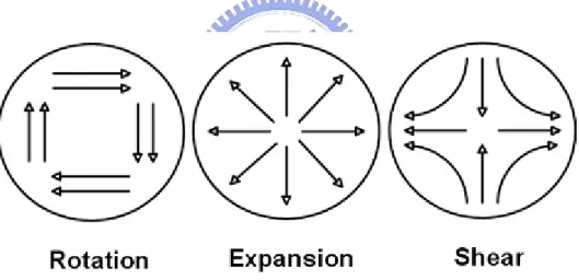
Fig. 1.2 Elementary flow components (EFCs) ... 5
CHAPTER 2
Fig. 2.1 Mead’s silicon retina... 9Fig. 2.2 The model of the outer-plexiform layer of retina. Reprinted from [10]... 9
Fig. 2.3 Andreou and Boahen’s silicon retina... 10
Fig. 2.4 BJT-based silicon retina...11
Fig. 2.5 The circuit diagrams of (a) NPN pseudo-BJT and (b) PNP pseudo-BJT and their device symbols ... 13
Fig. 2.6 Pseudo-BJT-based silicon retina. Reprinted from [8] ... 14
Fig. 2.7 The bi-directional correlation model ... 16
Fig. 2.8 Structure of a single pixel. Reprinted from [1]... 17
Fig. 2.9 Structure of the BJT-based retinal processing circuit. Reprinted from [1]... 18
Fig. 2.10 The architecture of this proposed focal-plane motion sensor. Reprinted from [1] ………...21
Fig. 2.11 The architecture of the proposed rotation sensor, in which consists of 104 pixels and forms five concentric circles. Reprinted from [8] ... 22
Fig. 2.12 The pixel structure of the rotation sensor. Reprinted from [8] ... 23
Fig. 2.13 The structure of MLE, in which is implemented by NAND gate. Reprinted from [8]... 24
Fig. 2.14 Pixel structure of the proposed retinal focal-plane sensor circuit. Reprinted
from [14] ... 25
CHAPTER 3
Fig. 3.1 The pixel structure of the shear sensor ... 29 Fig. 3.2 The structure of the retinal processing circuit ... 30 Fig. 3.3 The optical flow of (a) shear motion (b) reversed shear motion ... 31 Fig. 3.4 Four pairs of selected primary paths along with the positions of pixel on these
paths. In this figure, each star sign represents a single pixel... 33
Fig. 3.5 The distribution of smoothing network where each square means a pixel and
the bold line represents the connection between pixels by N-channel MOSFETs ... 34
Fig. 3.6 The architecture of the core circuit where 92 pixels are included. The pixels
which are connected by bold lines belong to the same primary path of shear motion and correlations are performed between immediate neighbors on the same path. ... 35
Fig. 3.7 The block diagram of the motion computation circuit ... 36 Fig. 3.8 Structure of whole chip which is divided into three parts, core circuit, motion
computation circuit and control generator... 38
Fig. 3.9 The timing diagram of control signals used to control the core circuit and
motion computation circuit... 39
Fig. 3.10 (a) The incident pattern where black squares represent pixels receive the
pattern while white are background; (b) Smoothing currents of whole pixel array where (x, y) is the location of pixels corresponding to that in (a)... 40
Fig. 3.11 The successive 11 sampled frames (a) to (k) of shear motion... 41 Fig. 3.12 The successive 11 sampled frames (a) to (k) of reversed shear motion ... 42
Fig. 3.13 Three patterns used to test if the translation is dismissed: (a) an edge (b) a car
and (c) Lenna ... 44
Fig. 3.14 The successive 11 sampled frames (a) to (k) of shear motion pattern that are
tested in post simulation ... 46
Fig. 3.15 Post simulation results of three serial outputs, ashear, arshear and aself, of
core circuit with displacements (a) 1/2 pixels per frame, and (b) 1 pixel per frame... 47
CHAPTER 4
Fig. 4.1 The measurement setup ... 49
Fig. 4.2 Photograph of (a) the first experimental shear motion sensor contains only the
core circuit, (b) the whole chip, and (c) a single pixel, of the shear motion sensor ... 51
Fig. 4.3 (a) Calculated velocities over 11 frames when the shear pattern moves at 0.06
mm/sec, 0.09 mm/sec and 0.18 mm/sec; (b) Deviations between calculated and actual velocities. The sampling rate is 3 Hz. ... 53
Fig. 4.4 (a) Calculated velocities over 11 frames when the reversed-shear pattern
moves at 0.06 mm/sec, 0.09 mm/sec and 0.18 mm/sec; (b) Deviations between calculated and actual velocities. The sampling rate is 3 Hz... 54
Fig. 4.5 11 successive frames of test patterns. From (a) to (k) represents 11 frames of
shear motion test patterns while (k) to (a) represents reversed-shear test patterns. ... 55
Fig. 4.6 (a) Calculated velocities when the test pattern shown in Fig. 3.13 (a), an edge,
moving to the right at different velocities; (b) Calculated velocity decrease to nearly zero as sampling frames increase. The image translates to the right at
Fig. 4.7 (a) Calculated velocities when the test pattern shown in Fig. 3.13 (b), a car,
moving to the right at different velocities; (b) Calculated velocity decrease to nearly zero as sampling frames increase. The image translates to the right at 0.27 mm/sec. The sampling rate is 3 Hz... 57
Fig. 4.8 (a) Calculated velocities when the test pattern shown in Fig. 3.13 (c), Lenna,
moving to the right at different velocities; (b) Calculated velocity decrease to nearly zero as sampling frames increase. The image translates to the right at 0.27 mm/sec. The sampling rate is 3 Hz... 58
Fig. 4.9 A diagram used to explain the ratio of the object velocity to the image
CHAPTER 1
INTRODUCTION
1.1 BACKGROUND OF BIO-INSPIRED SENSORS
Due to the different operational principles of motion detection algorithms, the focal-plane motion sensors can be distinguished into two main divisions, i.e. non-bio-inspired motion sensors and bio-inspired motion sensors. The non-bio-inspired motion sensors used the gradient-based (intensity-based) algorithm. The bio-inspired algorithms, including the token-based algorithm, the energy-based algorithm and the correlation-based algorithm, are used in bio-inspired sensors.
The gradient-based algorithm usually directly evaluates the local image velocity, so it may spend a lot of hardware to compute spatial and temporal gradients. Moreover, this algorithm is sensitive to the change of the ambient illumination. Therefore the gradient-based algorithm is not practical for VLSI implementation because of these drawbacks. The bio-inspired motion sensors thus have been developed and provide robust, compact, and accurate implementations.
The bio-inspired motion sensors mimic the functions of motion detection in the biological visual systems. According to neurophysiological and psychophysical data, motion analysis in the human visual system can be divided into several stages. First of all, the retina extracts the local motion cues and is the early processing unit of the human vision system. The retina is a tiny tissue which lies at the bottom of the eye
incident from the bottom, it passes through the transparent cells and is transformed into electrical signals by the photoreceptors at the top. The primary signal pathway proceeds from the photoreceptors in the photoreceptor nuclear layer through the synopses to the bipolar cells, and then to the ganglion cells. In some signal pathway, the ganglion cells receive signals from the amacrine cells. The horizontal cells are located just below the photoreceptors whereas the amacrine cells just above the ganglion cells. The horizontal cells mainly transform the photoreceptor output response into a function of average illumination in both time and spatial domains.
The outputs of ganglion cells are further sent to the first stage of visual cortex, primary visual cortex (V1), the component of motion that is orientated in a direction perpendicular to the orientated of elements in the image is extracted. The following stage is the middle temporal (MT) area where the local-motion vectors over portions of the image are combined to compute less local estimates of pattern translation. Finally, the neurons in the middle superior temporal (MST) area and in the fundus of superior temporal sulcus visual (FST) area integrate the estimation of translation motion from MT to compute more complicated non-local motions, such as global translation, expansion, rotation and shear.
The biological visual system shows excellent capability of motion detection. Therefore much research effort has been devoted into the bio-inspired motion sensors according to the characteristics of the biological visual system. The motion detection algorithms, including the token-based algorithm, the energy-based algorithm, and the correlation-based algorithm, have been proposed. In the token-based algorithm, the token must be very reliable and the image processing for token extraction has to be very accurately. Besides, the similarities between different tokens give rise to the correspondence problem. It confuses the subsequent computation and tracking of motion. The energy-based algorithm gives reliable measurement of velocity, but it requires lots of spatio-temporal filters and is difficult for VLSI implementation. Correlation-based algorithm is simple, robust and compact, and thus becomes the most practical algorithm for circuit implementation. The correlation-based algorithm is based on the idea that correlates a pixel with the neighboring pixels with certain time delay. If the time for which the image moves from a pixel to its neighboring pixel is equal to the delay time, then the intensity at output of the correlation is the greatest. Based on this concept, the correlation-based algorithm has the direction selectivity property, but additional computation is required to obtain the value of velocity. In 2002, Huang et al proposed a CMOS focal-plane motion sensor with modified correlation-based algorithm
further computes the value of velocity.
1.2 RETINAL PROCESSING CIRCUITS
The retinal processing circuits has been researched for a long time. The Mead’s silicon retina chip implemented the functions of outer-plexiform layer including photo receptor cells, horizontal cells and bipolar cells. In the Andreou and Boahen’s silicon retina model, it coupled the photoreceptors and horizontal cells by electrical synapses to achieve the high dynamic range. To considerate the integration with other integrated circuits, the BJT-based silicon retina is proposed. A more detailed review of several representative retinal processing circuits is addressed in Chapter 2.
Due to the superior image processing capability of the biological retina, retinal processing circuits have been developed to mimic the operational principles of biological retina. There are some major superior features of retinal processing circuit to the conventional CMOS and CCD image sensors:
(1) Global light intensity adaptation: In the natural environment, it has extremely high dynamic range. The variation of reflectance is in the order of 30 dB, but the variation of illumination is up to 180 dB in the natural scene [2]. This gives a great challenge for artificial image acquisition. With technique of circuits, the retinal processing circuits mimic the vertebrate retina to achieve high dynamic range.
(2) Local light intensity adaptation: By adaptive integration time or the global automatic gain control, conventional imagers can solve the dynamic range problem. The two methods, however, usually suffer from non-uniform illumination. It has been shown that retinal processing circuits could work well even under non-uniform illumination [3].
(3) Edge detection/enhancement: A simple resistive network usually is essential to perform approximately Gaussian smoothing function, which is meant to mimic
the function of the horizontal cells in biological retina. The original signal is subtracted by the smoothing output to enhance the edge [4].
(4) Data compression: Considerable data compression is realized with a foveated structure of image array which is found in the primate’s retina. This structure gives good resolution in the center to perform the complex image processing, while keeping a wide view field, with still enough resolution for rough, but valuable, image processing [5].
1.3 RESEARCH MOTIVATION AND ORGANIZATION OF THIS
THESIS
1.3.1 Research Motivation
Fig. 1.2 Elementary flow components (EFCs)
Mathematically, optical flows can be decomposed locally into div (or contraction/expansion), curl (or rotation), and def (or shear), up to a translation [6]. Rotation, expansion (or contraction) and shear (or deformation) are called Elementary Flow Components (EFCs) as shown in Fig.1.2. These invariants can be used to describe the relative motion between an observer and his surroundings, and also the 3D structure of the surroundings. On the other hand, some electrophysiological recordings of the cortical neuron of the monkey have revealed that some neurons in Medial Superior
Temporal (MST) area of the visual cortex are selective to rotation, expansion/contraction, combinations of these stimuli, and translation in a given direction. It has been observed that another group of neurons in the fundus of superior temporal sulcus visual area (FST) of visual cortex is sensitive to shear. While rotation and expansion determine the relative motion between the observer and his surroundings, shear depends only on 3D structure of the environment [7]. Therefore, to describe the more complicated motion, the motion sensor which has a new structure to detect EFCs is studied. In [8], a focal-plane rotation motion sensor is proposed but it is not enough to achieve the objective to detect the complex motion. The detection of shear has not been explored yet.
It is the aim of this thesis to overcome the difficulty of extracting the information of shear motion in the conventional focal-plane sensors. In order to fit shear motion model, the pixels of this proposed shear sensor are placed in a shear-motion structure to ensure the detection of shear-motion. The modified correlation-based algorithm is adopted to reduce the silicon area overhead of a single pixel as well as provide the information of the value of velocity. As the advantageous features addressed in the Section 1.2, the retinal processing circuit is used to be the image acquisition circuit so that the robustness and correctness of motion computation are enhanced. The focal-plane shear motion sensor is the first one in the literature that can detect shear.
1.3.2 Thesis Organization
This thesis contains five chapters. Chapter 1 introduces the background of the bio-inspired motion sensors in the first place. The motion analysis in the human visual system is addressed along with the structure and the functions of biological retina. Then, the concept and the advantages of the bio-inspired motion processing are discussed. Furthermore, the retinal processing circuits, which mimic the functions of biological retina, are described and the advantages are also described.
In Chapter 2, the reviews of the retinal processing circuits and the focal-plane motion sensors are given. In the review of the retinal processing circuits, the operational principles and circuit implementations of several representative retinal processing circuits are described. In the review of the focal-plane motion sensors, motion sensors which are based on the correlation-based algorithm are emphasized since this algorithm is adopted in the design of this thesis.
In Chapter 3, the architecture and circuit of the proposed shear sensor is presented. This design is mainly divided in to two parts, which include core and motion computation circuits. The operational principles are described from the image acquisition to motion computation method and eventually the direction as well as velocity determined. MATLAB simulations are also given in this chapter to confirm the direction-selectivity. The proposed design can recognize shear motion and further find out the displacement.
In Chapter 4, the measurement results are introduced. The chip is fabricated by a 0.35 µm double-poly-quadruple-metal CMOS process. The chip area is 2036 x 1765 µm2 and the area of a single pixel is 52.96 x 55.07 µm2
with a fill factor of 16%. It is tested under the shear and reversed-shear pattern moving at 0.06 mm/sec, 0.09 mm/sec and 0.18 mm/sec. The deviations are less than ± 10%. Three patterns, an edge, a car and the Lenna are used to confirm that this design is able to dismiss translation.
Finally, the conclusions of this thesis are summarized in Chapter 5. Some suggestions for the future works about the implementation of the shear motion sensor are addressed in the chapter.
CHAPTER 2
REVIEWS OF RETINAL PROCESSING CIRCUITS AND
FOCAL-PLANE MOTION SENSORS
2.1 REVIEW OF RETINAL PROCESSING CIRCUITS
(1) Mead’s Silicon Retina [9]
According to physiological recordings, the photoreceptors’ electrical response is logarithmic in light intensity over the central part of the photoreceptors’ range, as are the response of the other cells in the distal retina. Therefore in the Mead’s silicon retina as shown in Fig. 2.1, the photoreceptor has been implemented using parasitic phototransistors and diode-connected MOSFETs to perform the function of logarithmic compression of the photocurrent.
The connections between horizontal cells in most species are through gap junctions to propagate electronic spread. In this resistive continuous network, the lateral spread of information at the outer-plexiform layer is thus mediated. As illustrated in Fig. 2.1, the voltage at every point of the resistive network represents a spatially weighted average of the photoreceptor inputs. The less weight is given to the input which is from the farther away point in the network. The space constant of the network can be changed by either varying the conductance of the transconductance amplifier or the strength of the resistors. The effective area which the signals are averaged is changed along with the space constant.
The bipolar cell is implemented by a transconductance amplifier in Mead’s retina. It mainly amplifies the difference between the photoreceptor signal and the horizontal one.
Fig. 2.1 Mead’s silicon retina
(2) Andreou and Boahen’s Silicon Retina [10]
Fig. 2.2 The model of the outer-plexiform layer of retina. Reprinted from [10]
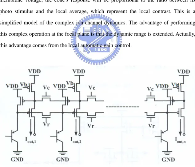
In this model, the photoreceptors are activated by light and produce activity in the horizontal cells through excitatory chemical synapses. The horizontal cells suppress the activity of photoreceptors through inhibitory chemical synapses. The photoreceptors and the horizontal cells are electrically coupled to their neighbors by electrical synapses. These allow ionic currents to flow from one cell to another, and are characterized by a certain conductance per unit area. In the biological system, contrast sensitivity, which means the normalized retinal output is proportional to local contrast, is obtained by shunting inhibition. The horizontal cells compute the local average intensity and modulated a conductance in the cone membrane proportionately. Since the current supplied by the cone outer-segment is divided by this conductance to produce the membrane voltage, the cone’s response will be proportional to the ratio between its photo stimulus and the local average, which represent the local contrast. This is a simplified model of the complex ion-channel dynamics. The advantage of performing this complex operation at the focal plane is that the dynamic range is extended. Actually, this advantage comes from the local automatic gain control.
Fig. 2.3 Andreou and Boahen’s silicon retina
junctions are realized using NMOS resistance while the chemical synapses are implemented using nonlinear transconductance. The photoreceptors R are implemented as nodes in the top layer of resistive network and the horizontal cells H as nodes in the lower layer. The two layers are coupled vertically using the two transistor current controlled current conveyers and laterally using resistive networks. A parasitic photo-BJT transforms light into current and further sources current to the photoreceptor nodes. At the same time, M2 sinks current from photoreceptor nodes. These operations thus realize the excitation and inhibition in the biological system. M1 sources current to excite the horizontal nodes. The bias current Ix at the source of device M1 determines the transconductance. Due to subthreshold operation of these devices, the voltages encode photocurrent logarithmically and result in a large optical dynamic range.
(3) BJT-based Silicon Retina [11]
In the BJT-based silicon retina architecture, the operation of the photoreceptor is realized by the parasitic PNP photo-BJTs in N-well CMOS technology with open bases. It is used to sense the light and generate photocurrents similar with photoreceptors. The resistive smoothing network, which is formed by connecting all bases of silicon retina array through MOSFETs, mimics the smoothing function of the horizontal cells. The two-dimensional silicon retina array is shown in Fig. 2.4. Each cell is consisted of an isolated PNP phototransistor as a photoreceptor and a smoothing PNP one as a horizontal cell. When the light is incident upon one cell, it is simultaneously incident upon the two floating bases of both phototransistors. The electron-hole pairs are generated at and nearby the depletion region of the two base-collector junctions. The generated electrons are swept into the base region by the force of the electric field in the depletion region, the holes are swept into the collector region and the excess electrons are diffused out through the MOSFETs resistor array in the following. The carrier diffusion and distribution results in the emitter currents of silicon retina array perform the smoothing function of vertebrate retina. The smoothing range can be adjusted by controlling the gate voltage of NMOS in Fig. 2.4. Therefore, the characteristic helps this structure overcome wide-ranging variations of intensity or contrast since MOS device provide a wide range of resistance values.
(4) Pseudo-BJT-based Silicon Retina [12]
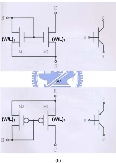
In the designs mentioned above, vertically parasitic PNP BJTs are used to implement functions of the photoreceptors and the horizontal cells. The common-emitter current gain of vertically parasitic PNP BJTs, however, decreases while the N-well CMOS technology moves toward more advanced. Thus the area of parasitic PNP BJT is usually enlarged to achieve the same current gain.
To solve the problem, a new circuit structure which is called pseudo-bipolar-junction-transistor (pseudo-BJT) is developed. Fig. 2.5 shows both the
circuit diagrams and symbols of NPN and PNP pseudo-BJTs. The NPN pseudo-BJT is composed of two n-type MOSFETs while the PNP is two p-type ones. The structure of pseudo-BJT is similar to the current-mirror circuit. Therefore the common-emitter current gain is approximately (W/L) 1/(W/L) 2 for NPN pseudo-BJT and (W/L) 3/(W/L) 4 for PNP. This gives a robustly and precisely current gain designed by adjusting geometric parameters of MOSFETs in the pseudo-BJT. The area is much smaller than that of a vertically parasitic BJT under the same current gain.
(a)
(b)
Fig. 2.5 The circuit diagrams of (a) NPN pseudo-BJT and (b) PNP pseudo-BJT and their device symbols
According to these superior features, pseudo-BJTs are more feasible than vertically parasitic BJTs to realize silicon retina. The PNP pseudo-BJT, Qi1, with a reversely biased photodiode, Dil, is used as the photoreceptor, while the NPN pseudo-BJT, Qi2,
(W/L)1 (W/L)2
with a reversely biased photodiode, Di2, and smoothing resistors R is used to form the retinal smoothing network, as shown in Fig. 2.6. The output signal, IOUTi, is the difference between collector currents of pseudo PNP BJT, Icil, and the pseudo NPN BJT, Ici2. The output current signals can be converted to voltage signals through suitable read-out circuits.
Fig. 2.6 Pseudo-BJT-based silicon retina. Reprinted from [8]
2.2 REVIEW OF FOCAL-PLANE MOTION SENSORS
Since motion provides rich information in understanding the environment, thus much research effort has been devoted into topics related to motion detection. In the conventional image processing system, it will create a heavy computational load for system even to perform the simplest task which human visual system can do. Therefore it has great difficulties to meet the requirements, which include inexpensive, low-power, compact, operation with a wide optical dynamic range, and working in real time, in the application for portable devices. There is a solution which is using application specific integrated circuits (ASICs) to overcome the heavy load of computation. In this approach, data transmission is still a bottleneck. Focal-plane image processing approach, which integrates the image acquisition and processing into a single chip [13], is therefore
developed to speed up data transmission between main function blocks.
The close interaction between image acquisition and processing units is the most salient feature of focal-plane image processing. Three levels of integration can be realized in focal-plane image processing: that is, processor per pixel, processor per column, and processor per chip. It is no doubt that the architecture of processor per pixel will provides the fully parallel and fastest image processing, but it may not be the optimum solution considering along with pixel area, fill factor, and power consumption.
To detect motion, the spatio-temporal processing has to be performed since motion analysis is related with both space and time. For the spatial image processing, each pixel has to interact with its neighboring pixels to extract spatial information. To perform the temporal image processing, image has to be stored in memory elements in a discrete-rime circuit while image is stored in delay elements in a continuous-time circuit. The number of memory or delay elements required in each pixel equals the number of past image frame needed in the processing. In most real implementations it is only practical to use one past image frame to prevent too many memories used.
The advantages of focal-plane motion processing include:
(1) Speed and parallelism: Focal-plane image processing has higher achievable processing speed than that of camera-processor combination. The reason is the
parallel structure between the imager and the processing unit and thus increased the data transfer bandwidth along with reduction of the data to be transferred. (2) Size: The close interaction between the image acquisition and processing units
allows a single chip implementation and achieves a compact system. Obviously, the size is smaller than the conventional implementations.
(3) Power dissipation: The focal-plane image processing makes use of analog circuits operating in the subthreshold region, the weak operating currents result in low power dissipation.
the trend in the future, this is a great advantage over the camera-processor option.
(5) High optical dynamic range: With the capability of spatio-temporal image processing, the focal-plane image processor can extract the average light intensity of the image and adjust the intensity of output to be adaptive to the average light intensity. Therefore, a high optical dynamic range can be achieved.
Ph1 Ph2
C1 C2 C3
D1 D2 D2 D3
Ph3
-
+
-
+
output1 output2 output3
Preferred direction with positive output Preferred direction with negative output
-+
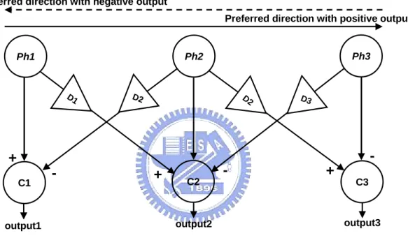
Fig. 2.7 The bi-directional correlation model
To detect motion, the motion detection algorithms adopted in focal-plane image processor include the gradient or intensity –based algorithm, the token-based algorithm, the energy-based algorithm, and the correlation-based algorithm. In recent years, studies have shown that correlation-based processes are responsible for motion detection in many animals, including humans. As addressed in Section 1.1, the correlation-based algorithm has superior features, that is, robustness and compactness. Therefore, this section puts more emphasis on the discussion of the correlation-based algorithm. Fig. 2.7 shows a correlation-based algorithm model which performs bi-directional correlations. Ph is the photo-circuit, D is a time delay element with a time delay, and C is the correlator. The
delayed signal is sent to the correlators in the neighboring pixels along preferred positive and negative direction paths. The sign of the output signal of the correlator depends on the direction of motion. When the object moves from Ph1 to Ph3 (Ph3 to Ph1), the correlator C2 outputs a positive (negative) signal. To make the output robust, the photo-circuits usually incorporate with certain spatial or/and temporal processing capability. Thus, the correlation is often performed on the features, e.g. edges, rather than the image itself.
In the following, some focal-plane image sensors are reviewed.
(1) A CMOS Focal-Plane Motion Sensor With BJT-Based Retinal Smoothing Network And Modified Correlation-Based Algorithm [1]
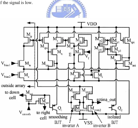
Fig. 2.8 Structure of a single pixel. Reprinted from [1]
In this design, it uses retinal processing circuits to sense image and further detect preferred global motion based on the modified correlation-based algorithm. Both
techniques on circuit implementation can overcome the delay time accuracy, limited tunable range of delay time and larger pixel area when both spatial and temporal edge detectors applied in conventional image sensors.
Fig. 2.8 is the structure of a single pixel used in this proposed sensor. Each pixel of the 32 x 32 array includes the BJT-based retinal processing circuit, two registers, five correlators, and five shift registers. After sensing image tested, the output of the retinal processing circuit is then sent to CF, which memorizes the current frame, and PF samples the data from CF after a clock cycle controlled by sample in Fig. 2.8. The output of CF is then correlated with the output of PF and the outputs of PF from its immediate neighbors. The outputs of the five correlators are next sent to shift registers to be accumulated by back-end accumulators. The shift register can receive the output of the correlators if the control signal is high while it can receive the data from the left pixel if the signal is low.
The implementation of the BJT-based retinal processing circuit is depicted in Fig. 2.9. An isolated photo-BJT is used as the photoreceptor, a smoothing photo-BJT with adjustable N-channel MOSFET resistors is used to form the retinal smoothing network, and a current-input CMOS Schmitt trigger and two inverters are included. The base of the smoothing photo-BJT is connected to the photo-BJT Q1’s four nearest neighbors, via the N-channel MOSFET resistors Msrd and Msrr, whose resistance is controlled by the gate voltage Vsmooth, forming the smoothing network. The transistors Mins, Mips, Mn and
Mini, Mipi, Mp are used to virtually bias the emitters of Q1 and Q2 at Vbias. Mip, Min, and
Mc are common to all pixels. The current-input CMOS Schmitt trigger comprises Ms,
Msr, Mi, Mir, Mf1, and Mf2 transistors. The voltage Vf is used to adjust the threshold level. The transistors Mp1, Mp2, Mp3, and Mp4 are used to mirror the emitter current of Q2 to the current-input CMOS Schmitt trigger. The inverters A and B amplify the output of the current-input CMOS Schmitt trigger to VDD or VSS so that the signal is converted from analog to binary.
The modified correlation-based algorithm is adopted in the proposed motion sensor. All the outputs of the correlator along the preferred direction are accumulated by the accumulator throughout the array to determine the correlation output. The correlation output is used to calculate the displacement in a sampling period. In the proposed motion sensor, the output of PF is shifted to the four nearest neighbors in the +x, -x, +y and –y directions so that the displacement along these four directions can be determined. The corresponding correlation outputs are C(+x), C(-x), C(+y), and C(-y), respectively. The correlation output between the output of PF without shift and the output of CF as defined by C(no) is also determined and is used to calculate the displacement. The five kinds of correlation outputs are further averaged over 16 sampling periods and are defined as Ca(+x), Ca(-x), Ca(+y), Ca(-y), and Ca(no), respectively. The calculated displacement Δx in the +x or –x direction normalized to the distance between two
(2.1)
Similarly, displacement Δy in the +y or –y direction can be expressed as
(2.2)
The direction of motion can be determined by comparing the amplitude of Ca(+x) with that of Ca(-x) as well as Ca(+y) with that of Ca(-y). The directional angle is given by
If the displacement and direction of motion is calculated without using the averaged correlation outputs, the pattern-related deviations are significant. Besides, this also helps to express the displacement between 0 and P. Since each pixel is correlated only with the nearest neighbors, it is a criterion that the displacement per frame of the image under test cannot exceed P.
Notably, during shifting of the previous image frame, the boundary pixels are fixed at zero for simplicity. Therefore, the correlation at the boundary yields errors when calculating Ca(+x), Ca(-x), Ca(+y), and Ca(-y). The boundary condition, however, does not influence the calculation of Ca(no) since no shifting is introduced in the calculation of Ca(no). To calibrate this boundary condition, two factors b1 and b2 are added to (2.1) and (2.2).
(2.4)
(2.5) The value of b1 is chosen to be half the number of pixels at one side of the boundary while b2 is half of b1.
( )
[
]
( )
( )
{
}
( )
( )
{
}
2 * , , x x a x x a a x a a x M m P C no m M MAX C x C x m min C x C x ∆ = − − ≡ + − ≡ + −( )
( )
( )
{
}
( )
( )
{
}
2 * , , y y a y y a a y a a M m y P C no m M MAX C y C y m min C y C y − ∆ = ⎡ − ⎤ ⎣ ⎦ ≡ + − ≡ + − tan y y x x M m y x M m θ =∆ = − ∆ − (2.3)( )
[
]
( )
1 2 1 2 2 * 2 * x x a x y y a y x M m b P C no m b M m b y P C no m b ∆ = − + − − − + ∆ = ⎡ − − ⎤ ⎣ ⎦ tan y y x x M m y x M m θ =∆ = − ∆ − (2.3)Fig. 2.10 illustrates the architecture of the proposed focal-plane motion sensor, which includes the 32 x 32 pixel array and the peripheral circuits, including five sets of 6-b accumulators for each row, and five sets of 11-b accumulators. The data in the five 11-b accumulators are read out as C(+x), C(-x), C(+y), C(-y), and C(no), respectively. The average, displacement, and direction are calculated off-chip by software.
Fig. 2.10 The architecture of this proposed focal-plane motion sensor. Reprinted from [1]
This work presents a real-time CMOS focal-plane motion sensor that uses the BJT-based retinal processing circuit and a modified correlation-based algorithm. The correlation-based algorithm is modified and therefore applied to calculate the velocity and direction. The BJT-based retinal processing circuit is used to acquire images and enhance contrast. The presented motion sensor greatly reduces the deviation of the calculated displacement and direction for different image pattern by averaging correlation results over 16 frame-sampling periods
(2) Analysis and Design of a CMOS Angular Velocity- and Direction-Selective Rotation Sensor With a Retinal Processing Circuit [8]
In this design, the CMOS focal-plane rotation sensor uses the same retinal processing circuit with [1] to preprocess the incident image and the correlation-based algorithm to detect the local motion vectors.
Fig. 2.11 The architecture of the proposed rotation sensor, in which consists of 104 pixels and forms
five concentric circles. Reprinted from [8]
In most of the focal-plane motion sensors, the spatial distribution of the pixels forms regular and rectangular pattern and the correlation is performed between the two adjacent pixels to get the local motion vectors. This structure, however, has difficulty to extract more complex motion vectors than those in translation, such as Elementary Flow Components (EFCs). To find the solution to extract the information of rotation, the pixels of the proposed rotation sensor are placed in a polar structure to detect the global
rotation direction and velocity of the rotating images. Fig. 2.11 shows the architecture of the proposed rotation sensor, which consists of 104 pixels and forms five concentric circles. Every pixel is correlated with the clockwise and counterclockwise pixels that are 45o apart. The clockwise or the counterclockwise correlation results of all the pixels in the same circle are sent to MLE, which is implemented by a NAND gate, to determine the velocity and direction of the global rotation. There are two sets of MLE, corresponding to clockwise and counterclockwise rotation detection, for a single circle.
Fig. 2.12 The pixel structure of the rotation sensor. Reprinted from [8]
Fig 2.12 shows the structure of a single pixel. Each pixel consists of a retinal processing circuit, two registers, two correlators, two P-channel MOSFETs, which are parts of NAND gates as the MLE. This structure is similar to that of [1] addressed previously except the back-end processing circuit to deal with ouputs of correlators. In this rotation motion sensor, it uses MLE, which is implemented by a NAND gate, instead of accumulators. Fig.2.13 illustrates the structure of MLE with fan-in number
equal to the total number of pixels in a circle. The p-channel MOSFETs of the NAND gate are located inside each pixel, i.e. Mmlecc and Mmlec in Fig. 2.13. The outputs of correlator in each pixel are sent to the gates of Mmlecc and Mmlec as shown in Fig. 2.13. The drains of Mmlecc (Mmlec) of all the pixels in the same circle are connected together to the diode-connected N-channel MOSFET Mnload as the load to generate the counterclockwise (clockwise) MLE output. The output of MLE is at logic 0 if the outputs of all correlators are at logic 1, which means the local motion vector is detected.
Fig. 2.13 The structure of MLE, in which is implemented by NAND gate. Reprinted from [8]
To calculate the velocity of rotation, the times that the output of MLE is at logic 0 are recorded within 80 clock cycles and a parameter R is defined as
number of logic 0 of MLE output (%) 100
80
R = × (2.6)
R reaches maximum if the image is rotated with the selected angular velocity and
decreases if angular velocity is deviated from the selected one. The relationship between
R and angular velocity ω is related with the number of pixels in a circle as well as the
number and the position of the edges of the image.
The advantageous characteristics of the proposed rotation sensor are high dynamic range, real-time image processing, and a wide-range of detectable angular velocity. The
proposed rotation sensor is appropriate for applications like the real-time and remote detection of the rotation of automobile engines and wheels, motors, microscopic rotating images, etc.
(3) A Low-Photocurrent CMOS Retinal Focal-Plane Sensor With a Pseudo-BJT Smoothing Network and an Adaptive Current Schmitt Trigger for Scanner Applications [14]
Fig. 2.14 Pixel structure of the proposed retinal focal-plane sensor circuit. Reprinted from [14]
The BJT-based retinal sensor chip mimics parts of functions of the cells in the outer plexiform layer of the real retina. As in the real retina, the retinal sensor chip has similar advantageous features, such as high noise immunity, edge enhancement, and high dynamic range. Therefore, the BJT-based retinal structure has been proven that it is very compact and suitable for VLSI implementation. However, the parasitic p+-n-well-p-substrate BJTs used in the BJT-based retinal sensor have a smaller current
gain when the N-well CMOS technology scaling down to 0.25 µm or below as well as the chip area of the parasitic BJT is large as described in Section 2.1. To solve the problems mentioned above, a new circuit structure is developed and called the pseudo-BJT (PBJT) [12]. By incorporating Pseudo-BJT along with adaptive current Schmitt trigger, it not only solves the problems which the parasitic BJT has but in addition has advantages of low operational photocurrent levels (pA) and robust noise immunity. Besides, this proposed retinal sensor operates in the subthreshold region. Therefore, the circuit just consumes little power during in nonlighting mode. The proposed structure enhances noise immunity and eliminates disturbances.
In the proposed pixel structure of a retinal focal-plane sensor, as shown in Fig. 2.14, an isolated PNP pseudo-BJT is used as photoreceptor, a smoothing NPN pseudo-BJT with adjustable N-channel MOSFET resistors is used to form the retinal smoothing network, an adaptive current Schmitt trigger, and an inverter are included. The transistors Mp1, Mp2, and photodiode are as the PNP pseudo-BJT. The transistors Mn1, Mn2, and a photodiode are as the NPN pseudo-BJT with four adjustable N-channel MOS resistors Ms1-Ms4 as the smoothing network. The smoothing network is connected to its four neighbors, and the resistance of four MOS resistors is controlled by the gate voltage Vsmooth (VF). The adaptive current Schmitt trigger is composed of Mp1, Mp2, Mn1, and Mn2, and hysteresis level adjustment Mpf1, Mpf2, Mnf1, and Mnf2. The current Iiso is the generated current of PNP pseudo-BJT whereas the current Ismt is that of NPN pseudo-BJT. The operation principle of the adaptive current Schmitt trigger is introduced as follows: initially, if the current Ismt is bigger than the current Iiso, the Vout (Retina_out) goes too high and it turns on the MOS Mnf2 to draw the current ∆I/2. By the same token, the current Ismt is smaller than the current Iiso at first, the Vout (Retina_out) stays low level and it turns on the MOS Mpf2 to sink the current ∆I/2. Therefore there is a ∆I current hysteresis. If the induced photocurrent is larger, the current of transistors Mn1 and Mp1 becomes also larger. Due to the function of current mirror Mn1-Mnf1 and Mp1-Mpf1, the current of Mnf1 and Mpf1 could be adjusted by the
induced photocurrent. Hence, this proposed circuit could adjust the current adaptively without external controlling voltage. The transistors Mp and Mn are composed of an inverter to amplify the output of the adaptive current Schmitt trigger to VDD or GND so that the signal is converted from analog to binary.
CHAPTER 3
CIRCUIT DESIGN AND SIMULATION RESULTS
3.1 DESIGN CONSIDERATION
As mentioned in Section 1.3.1, some neurons in Medial Superior Temporal (MST) area of the visual cortex are selective to rotation, expansion/contraction, combinations of these stimuli, and translation in a given direction in the cortical neuron of the monkey. It has been observed that another group of neurons in the fundus of superior temporal sulcus visual area (FST) of visual cortex is sensitive to shear. While encountering complex non-local motions, the neurons in both visual cortex areas integrate the estimation of translation motion from the middle temporal (MT) area to detect these motions, such as global translation, expansion, rotation and shear.
In conventional focal-plane motion sensors, however, the arrangement of the pixels is regular and forms a rectangular pattern. Also, the correlation is performed between the four immediate neighbors to obtain the local motion vectors. These sensors are designed for translation [1] but not suitable for EFCs detection because of their special motion model. In order to fit shear motion model, the pixels of this proposed shear sensor are placed along the shear-motion paths to ensure the detection of shear-motion. Every pixel is correlated with the shear and reversed-shear pixels that are neighbored apart in the same path, which will be shown in the next Section. Based on the motion computation method of modified correlation algorithm [1], shear motion can be detected and dismiss other motions. Displacement and velocity are also determined bycomputation of summations of all correlation outputs.
In the proposed shear sensor, the function of image acquisition and preprocessing can be performed by using the pseudo-BJT-based retinal processing circuit with an adaptive current-input Schmitt trigger [14]. It has the advantages of pseudo-BJT as well as the robust noise immunity, high dynamic range and contrast-enhanced.
3.2 CORE CIRCUIT REALIZATION
Fig. 3.1 The pixel structure of the shear sensor
Fig. 3.1 shows the structure of a single pixel. Each pixel consists of a retinal processing circuit, two registers, and three correlators. As shown in Fig. 3.1, after preprocessing by the retinal processing circuit, the register CF samples and stores the output of the retinal processing circuit and shift the stored data to the register PF after a clock cycle. The output of register CF is then sent to the correlators of the same pixel to be correlated with the output of PF and the outputs of PF from its adjacent pixels,
the correlators are corresponding to the detection of shear and reversed-shear motions and the other is used to adjuvant the computation of displacement. These outputs of the correlators are sent to the three accumulators followed the order selected by a decoder.
Fig. 3.2 The structure of the retinal processing circuit
The retinal processing circuit is illustrated in Fig. 3.2, in which an isolated PNP pseudo-BJT is used as a photoreceptor, a smoothing NPN pseudo-BJT with adjustable N-channel MOS resistors is used as the retinal smoothing network, an adaptive current-input CMOS Schmitt trigger and an inverter are included. It mimics parts of functions of the cells in the outer plexiform layer of the real retina. The retinal processing circuit converts incident images to bi-level images and therefore has properties of high dynamic range and contrast-enhanced. With aid of adaptive current Schmitt trigger, the ability of noise immunity is adjustable adaptively according to the value of induced photocurrent. Mismatch problem will cause the noise immunity range not symmetric but will not result in wrong output of this unit. The purpose of additional output, image_out, is used to monitor the image captured.
-15 -10 -5 0 5 10 15 -15 -10 -5 0 5 10 15 -15 -10 -5 0 5 10 15 -15 -10 -5 0 5 10 15 (a) (b)
(a)
(c)
(d)
The optical flow of pure shear, which is defined as a contraction in one and an expansion in the orthogonal direction, such that area is conserved, is shown as Fig. 3.3. In Fig. 3.3(a), the optical flow on x-axis is in contraction direction while y-axis is in expansion direction. The directions in Fig. 3.3(b) are opposite to those in (a). Therefore, if (a) is defined as shear motion, (b) is reversed shear motion. To detect shear motion, it is necessary to arrange the positions of pixel along the shear-motion paths. First of all, find several primary paths according to the optical flow of shear motion. In this design, four symmetry pairs of path are found and furthermore each pixel is placed along these selected primary paths. It is also important to keep the tangential distance between two pixels in the same path equal. If not, it is difficult to extract the information of displacement or velocity of shear motion. Four pairs of selected primary paths along with the positions of pixel on which are illustrated in Fig.3.4.
Fig. 3.5 The distribution of smoothing network where each square means a pixel and the bold line represents the connection between pixels by N-channel MOSFETs
While constructing the pixel array in the proposed shear motion sensor, since the arrangement of pixels is not regular and not a rectangular pattern, the connection of smoothing network is thus not as regular as those in the motion sensors designed for other motions [1], [8], [11], [14]. In order to achieve the two-dimensional smoothing function, the connection of N-channel MOSFETs between retinal processing circuits must be in the most symmetric and uniform manner. Based on this principle, the distribution of the smoothing network in this proposed sensor is shown in Fig. 3.5.
Fig. 3.6 The architecture of the core circuit where 92 pixels are included. The pixels which are
connected by bold lines belong to the same primary path of shear motion and correlations are performed between immediate neighbors on the same path.
To satisfy the two main distinguished characteristics addressed above, the arrangement of pixels is as Fig. 3.6 for fulfilling the detection of shear motion. Fig. 3.6
shows the architecture of the proposed shear sensor, which consists of 92 pixels and form four shear-motion detection pairs. Each pair is composed of four sets of pixels placed in symmetric manner to correspond to the shear motion as described in Fig. 3.4. Every pixel is correlated with itself and the shear and reversed-shear pixels that are neighbored apart. The shear, reversed-shear and self correlation results of each pixel are connected to form three primary outputs, ashear, arshear and aself, respectively, and fed to the three accumulators in motion computation circuit.
3.3 MOTION COMPUTATION CIRCUIT DESIGN
Fig. 3.7 The block diagram of the motion computation circuit
Based on the motion computation method of modified correlation algorithm proposed in [1], shear motion can be detected and dismiss other motions. The three primary outputs, ashear, arshear, and aself, of the core circuit are thus accumulated to obtain three correlation outputs which are used to determine the displacement per frame. Followed the motion computation method of [1], the displacement of shear motion can be obtained by
(
)
(
)
(
)
{
}
(
)
(
)
{
}
2 * , , P M m P C self mM MAX C shear C rshear
m min C shear C rshear
∆ − = ⎡ − ⎤ ⎣ ⎦ ≡ ≡
∑
∑
∑
∑
∑
(3.1), where C(shear), C(rshear) and C(self) represent the sum of ashear, arshear and aslef which are generated sequentially by whole pixel array in a sample frame. To realize the computation by circuits, three 10-bits accumulators, one comparator, two multiplexers, two subtractors and an integer divider are used to perform the formula shown above. Fig. 3.7 illustrates the block diagram of motion computation circuit used in this design. The 10-bits accumulator collects 0’s of the serial input and needs 92 clock cycles to complete accumulation of whole pixel array in a sample frame. A comparator and two multiplexers are used to determine M and m shown in formula. In the next step, two subtractors calculate both divider and dividend. An integer divider is adopted in this design to obtain the final computation result. To achieve the accuracy to two digits under the floating point in decimal, the dividend needs to be shifted 6 digits left in binary before fed in the integer divider. The quotient obtained by the integer divider therefore must be shifted 7 digits right in binary to get the correct result. To calibrate the boundary condition, two factors b1 and b2 can be added and (3.1) will become
(
)
(
)
(
)
{
}
(
)
(
)
{
}
1 2 2 * , , M m b P P C self m bM MAX C shear C rshear
m min C shear C rshear
− + ∆ = ⎡ − − ⎤ ⎣ ⎦ ≡ ≡
∑
∑
∑
∑
∑
(3.2)In this design, b1 is 8 and thus b2 is 4. To implement the calibrating factors in the motion computation circuit, it simply replaces two two-input subtractors with three- input ones. b1 is inverted and as the third input of the upper subtractor while b2 is the third input of the lower one.
computation circuit further calculates the displacement according to the three primary outputs of the core circuit. There is another part of circuit, control generator, to create the appropriate clock signals for both the core and the motion computation circuits. The core circuit is designed by full-custom flow while the others are by cell-based flow. The timing diagram of the control signals generated by control generator is illustrated as Fig. 3.9. In this diagram, system clock is the main clock signal fed in whole system. By adjusting system clock, the operating frequency of the proposed shear motion sensor can be tuned. Every 200 clock cycles of system clock makes a sample frame, and first 100 clocks are preserved for the core circuit to complete its work while the other clocks are used to accumulate correlation outputs of 92 pixels generated in a sample frame. Therefore, control generator enables core enable to generate core clock which shifts image sampled last frame to PF in the core circuit, and enables ALU enable to generate 92 clocks which drive accumulators to collect correlator outputs.
Fig. 3.8 Structure of whole chip which is divided into three parts, core circuit, motion computation circuit and control generator
Fig. 3.9 The timing diagram of control signals used to control the core circuit and motion computation circuit
3.4 SIMULATION RESULTS
Table 3.1 The designed device dimension and the bias voltages of the retinal processing circuit
Mp1 (W/L) 1µm/1µm Mp2 (W/L) 20µm / 1µm Mpf1=Mpf2 (W/L) 2µm / 1µm Mn1 (W/L) 1µm / 1µm Mn2 (W/L) 20µm / 1µm Mnf1=Mnf2 (W/L) 5µm / 1µm Ms1=Ms2=Ms3 (W/L) 1µm / 1µm Mpi (W/L) 0.4µm / 0.35µm Mni (W/L) 0.4µm / 0.35µm vs adjustable
The dimensions of the MOSFETs in the retinal processing circuit using in the proposed design are summarized in Table 3.1. These dimensions may be further
optimizes to make the pixel size smaller and more practical. (b) (a) 1 2 3 4 5 6 7 8 9 10 11 1 2 3 4 5 6 7 8 9 10 11
Fig. 3.10 (a) The incident pattern where black squares represent pixels receive the pattern while white
are background; (b) Smoothing currents of whole pixel array where (x, y) is the location of pixels corresponding to that in (a)
To present the smoothing function of this irregular smoothing network in this design, a pattern which is shown in Fig. 3.10 (a) is incident. In (a), each square represents a pixel and black squares are pixels which receive the pattern while white do not. Fig. 3.10 (b) shows smoothing currents versus (x, y), the location of pixels corresponding to that in (a). The simulation is under the condition of 100nA photocurrent and 1-volt smoothing voltage.
Fig. 3.12 The successive 11 sampled frames (a) to (k) of reversed shear motion
To ensure the modified correlation-based algorithm can detect the preferred motion, MATLAB simulations were performed on some patterns moving towards translation or shear directions. In real world, no rigid objects do pure shear motion and therefore the test pattern needs to be generated by software. Fig. 3.11 shows a pattern moves towards the direction of shear and are sampled by pixels to obtain the successive 11 frames (a) to (k). Table 3.2 summarizes the three main correlation outputs obtained by MATLAB
with different displacement per frame. As shown in Table 3.2, the calculated displacement according to the modified correlation-based algorithm is 0.87 pixels per frame when the test pattern moves 1 pixel per frame. When the real displacement is 0.25 pixels per frame, the simulation result is 0.2 pixels per frame. With calibration, 0.87 can be improved to 0.93 and 0.2 to 0.23. Fig. 3.12 is a pattern used to test the direction-selectivity of reversed shear motion. Table 3.3 gives the simulation results of Fig. 3.12. Comparing the correlation outputs of Table 3.2 and 3.3, the characteristics of direction selectivity is confirmed since the correlation output of shear direction is greater than that of reversed shear if the test pattern moves towards shear direction, and the correlation output of shear direction is fewer than that of reversed shear if the test pattern moves towards reversed shear direction.
Table 3.2 MATLAB simulation results of Fig. 3.11, where the calculated displacement with and without calibration are given
Table 3.3 MATLAB simulation results of Fig. 3.12, where the calculated displacement with and without calibration are given
ΣC(shear) ΣC(rshear) ΣC(self) ∆P/P
(with calibration) deviation (with calibration) D=1 pixel/frame 0 214 122 0.87 (0.94) 13 % (6%) D=1/4 pixels/frame 128 192 288 0.2 (0.23) 20 % (8%)
ΣC(shear) ΣC(rshear) ΣC(self) ∆P/P
(with calibration) deviation (with calibration) D=1 pixel/frame 214 0 122 0.87 (0.94) 13 % (6%) D=1/4 pixels/frame 192 128 288 0.2 (0.23) 20 % (8%)
Fig. 3.13 has three patterns used to test if the proposed shear motion sensor can dismiss translation. Fig. 3.13(a) is a pattern of an edge while (b) is a simple car figure and Fig. 3.13(c) is a pattern, Lenna. First two are simple and the other is a more complicated benchmark pattern. Tables 3.4 to 3.6 summarize the MATLAB simulation results of patterns shown in Fig. 3.13. Two translation displacements, 1 and 1/7 pixel per frame, are simulated and the calculated displacements, including those with and without calibration, are nearly 0 no matter what test patterns. These simulation results ensure the proposed architecture of shear motion sensor has the direction selectivity and thus can distinguish shear motion from other motions.
![Fig. 2.6 Pseudo-BJT-based silicon retina. Reprinted from [8]](https://thumb-ap.123doks.com/thumbv2/9libinfo/8229075.170840/27.892.135.765.345.700/fig-pseudo-bjt-based-silicon-retina-reprinted.webp)
![Fig. 2.13 The structure of MLE, in which is implemented by NAND gate. Reprinted from [8]](https://thumb-ap.123doks.com/thumbv2/9libinfo/8229075.170840/37.892.150.749.411.726/fig-structure-mle-implemented-nand-gate-reprinted.webp)
