國
立
交
通
大
學
電子工程學系 電子研究所
博 士 論 文
前 瞻非 揮發 性電 阻式 記憶 體元 件之 製作 與特 性研 究
Fabrication and Characterization of FeO
xBased Resistive Random Access
Memory
研 究 生:馮立偉
指導教授:張俊彥 教授
前瞻非揮發性電阻式記憶體元件之製作與特性研究
Fabrication and Characterization of FeO
xBased Resistive Random Access
Memory
研 究 生:馮立偉 Student:Li-Wei Feng
指導教授:張俊彥 Advisor:Chun-Yen Chang
國 立 交 通 大 學
電子工程學系 電子研究所
博 士 論 文
A DissertationSubmitted to Department of Electronics Engineering and Institute of Electronics
College of Electrical and Computer Engineering National Chiao Tung University
in partial Fulfillment of the Requirements for the Degree of
Doctor of Philosophy in
Electronics Engineering
November 2010
前瞻非揮發性電阻式記憶體元件之製作與特性
研究
研 究 生: 馮 立 偉
指導教授: 張 俊 彥 院士
國 立 交 通 大 學
電子工程學系暨電子研究所
摘要
隨著數位行動生活的到來,非揮發性記憶體在可攜式電子產品,如:手機、 數位相機跟筆記型電腦扮演著重要的角色。以傳統浮閘(Floating gate)記憶體為基 本元件之非揮發性固態半導體記憶體是現今非揮發性記憶體的主流,但是它有著 許多缺點,包含:高的操作電壓、低的操作速度與較差的耐久力,且隨著尺寸微 縮的趨勢下,面臨了難以解決之難題,即儲存在懸浮閘極中之電荷,因穿遂氧化 層過薄而隨時間漸漸流失,造成資料流失,如此瓶頸,加快了下世代非揮發性記 憶體之研究腳步。其一類預期能取代傳統浮閘記憶體的非揮發性元件者為電阻式 非揮發性記憶體(RRAM),主要是由於其製程簡單且與動態隨機存取記憶體 (DRAM)製程相似,可以被整合到半導體的後段製程。電阻式記憶體擁有高速、 非揮發性與低電壓操作的特性等優點。故本論文所研究之主題,將針對電阻式性 記憶體這類型之非揮發性記憶體原件觀念為主,而提出一以鐵原素為製程基礎之 一系列具簡易製程方式的記憶體原件之備製,並探討其元件之原理與特性,以及 更進一步地提供改良其元件特性之製備方式:對此鐵原素電阻式性記憶體而言,我們提供了一種利用氧化鐵電極的表面之方式,來獲得一層具備阻值轉態特性的 薄氧化鐵薄膜,因為阻值轉態特性的存在主要與非完全化學當量組成的過渡金屬 氧化物的存在相關,是故藉由氧化鐵電極表面所獲得之薄氧化鐵薄膜的最大優勢 為其本身所具備之不完全化學組成之氧化層成分,而能利用以提供較佳的電阻式 記憶體特性。另一方面,藉由鉑(Pt)元素於鐵電極的參雜而製成的鉑化鐵(FePt alloy)合金,而能間接控制鐵電極的氧化與擴散,以利於進一步地探討其特性與 原理。就其基本轉態原理之推測上,我們藉由不同極性之高壓施加而於電極上所 產生之不同特性之泡泡現象(Bubble Effect),以及元件電阻值對不同元件電極面 積之關係分析,來更進一步來間接地佐證此氧化鐵之阻值轉態現象的機制。甚 者,我們亦於此兩組含鐵電極之元件,研究於不同的後續熱退火製程處理之特 性,發現藉由退火處理能有效地降低形成電壓、操作電壓以及其電性參數之變異 性,而能獲得更佳的電阻式記憶體特性,其原因也藉由 X 光光電子能譜儀(XPS), 穿透式電子顯微鏡(TEM),X 光粉晶繞射儀(XRD)分析來討論;我們更藉由做不 同退火處理樣本之電性結果的統計分析,來釐清其更深入的機制。此外,我們亦 發現藉由設定量測時之電流限流限制條件與電壓掃描限制條件之設定,而能任意 調整此氧化鐵薄膜其所具有的阻值狀態,能達到具多重阻值位階之特性,以利於 成為高儲存資料密度之運用;同樣地,此不同電流限流與電壓掃描限制條件下之 電性結果統計分析,亦能對這尚未完全明瞭的電阻轉態機制,進一步地來輔助此 元件轉態機制之確認。最後對全文作一總結,並對未來可行的研究工作做一建議。
Fabrication and Characterization of FeO
xBased
Resistive Random Access Memory
Student: Li-Wei Feng
Advisor: Dr. Chun-Yen Chang
Department of Electronics Engineering & Institute of Electronics,
National Chiao Tung University
Abstract
With the arrival of Digital Age, nonvolatile memory (NVM) plays an important role in portable electronic products, such as the mobile phone, digital camera, and notebook computer. Floating gate composed nonvolatile memories have been widely applied in electronic devices in recent years, but it has many drawbacks, including high operation voltage, low operation speed, and poor endurance. Moreover, as the device dimensions are continuously scaled down, the floating gate composed memory faces the challenge of thin tunneling oxide that causes an unsatisfactory retention time. Consequently, resistive random access memory (RRAM) is one promising candidate to substitute for conventional floating gate memory. As for RRAM, the digital data can be stored in two memory states with high and low resistivities, ON-state and OFF-state, respectively. The two memory states can be easily switched by voltage biases or pulses, which enhance the possibility of the application in circuit level. Therefore, the topic of this thesis discusses this advanced nonvolatile memory devices by fabricating and characterizing iron-based RRAM devices and, furthermore, proposes the methods to improve the characteristics of the proposed devices for NVM applications. The proposed iron-based RRAM device was fabricated by a structure of
and produced spontaneously during the plasma-enhanced tetraethyl orthosilicate oxide deposition process due to the ease of oxidation of iron atoms. The basic idea of the proposed structure is that the resistive switching effect is associated with the existence of nonstoichiometric materials, so the thin FeOx transition layer produced by partially
oxidizing the iron electrode surface exhibits a richer nonstoichiometry property because of containing the compositions varied from Fe-rich FeOx (close to Fe
electrode) to oxygen-rich FeOx (close to SiO2 layer). Moreover, in order to clarify the
detailed mechanism of resistive switching effects, a method of adding platinum (Pt) into Fe electrode, which affects oxidation and diffusion characteristics of Fe layer, was also proposed by a TiN/SiO2/FeOx/FePt structure. In addition, observation of
bubble effects occurred at the top electrode after biasing highly opposite polarity voltage stresses as well as the electrode area dependence of resistance values also provides another indirect method to clarify the mechanism of resistive switching effects.
Moreover, the influence of thermal annealing treatments on the FeOx resistance
switching behaviors was also researched because of the thermal sensitivity of the iron oxide layer. The distinct reduction of memory switching parameters in forming voltage, set/reset voltages, and even their dispersions was obtained after annealing. The cause was also discussed by XPS, TEM, and XRD analyses. Additionally, statistical electrical results, including set/reset current, set/reset voltage and set/reset power, also help for understanding the mechanism of resistive switching effects.
Furthrmore, multiple resistance states were easily observed to obtain in our proposed FeOx-contained structure by justifying the sweeping voltage during the reset
more details to clarify the mechanism of the FeOx-contained resistive switching
behaviors.In the final part of this dissertation, the conclusions and the suggested future works are presented.
誌謝
從歷歷在目之初至新竹念研究所之時,轉眼間便就到了該好好寫此篇夾在 博士論文內之致謝之際,但此當中,卻又矛盾地充滿著一日三秋所感受到的喜、 怒、哀、樂,與悲、歡、離、合,確如人飲水般,讓我充實的體會了一遍。而此 一切的一切,著實都是因為有著的大家幫忙與協助始得以完成,是故希望能藉由 此篇致謝,來拙劣地敘述出我內心所存著無限感謝的一小部分。 首先,很感謝的是我親愛的父母親,正因有你們從小到大無悔付出的養育, 而讓我得以獲得此次寶貴求學進修之機會與經驗;同時,也很感謝在此求知過程 中,不辭辛勞地給予諄諄教誨的指導老師張俊彥導師,不管是專業領域、或是待 人處事上的栽培與教導,正深深地影響著之後我所需要的一切。我人生中正因有 你們如貴人般在旁的提攜與指導,才有我如今一切的我,因此除了感謝還是感 謝。我也要感謝口試委員張鼎張教授、鄭晃忠教授、龔正教授、吳永俊教授、詹 益仁組長、高明哲副組長與崔秉钺教授的指導與提醒,讓論文的內容更趨完善。 同時,也很感謝在課業與實驗上指導與幫忙的學長姐們、同學們以及學弟 妹們,雖然我知道這種概括的寫法很簡略,但對你們感謝之心,卻正如此無法一 一明列名子般之無以細數的多,而得以讓我能在學業方面順利修完課程,在實驗 方面也得到很多寶貴的經驗與研究成果:學長姐當中,又想特別再次提出幾位對 我直接影響重大而得鄭重感謝的人,包括陳紀文、楊宗熹、吳永俊、涂峻豪、陳 世青、陳怡誠、陳致宏、郭柏儀學長等等,以及幾位跟我共同切磋的好同學,包 括林昭正、陳弘斌、鄭兆欽、揚哲育、何武陵等等,學弟妹方面,包括涂博閔、 王派璿、薛培堃、翁麗雯、陳弘根、李勝凱、蔡佳州、江培維、莊凱麟、張耀峰、 張哲榮、林聖錡、陳緯仁、胡志瑋、王信淵、蔡侑廷、陳仕承、張冠張、陳敏甄、 俞詠騰,尤書鴻,與實驗室優秀的助理等等,感謝你們一路上的陪伴與幫忙,讓 我能完成這個修業學程。 最後還是在一次謝謝指導老師張俊彥老師的幫忙與指導,讓我重新認清自 己的缺點,也讓我體驗到自己能力的渺小,體驗到仍有很多東西該學該做,我想 這種課外的指導才是我這次學習中最有價值的東西。 2010.11Contents
Chinese Abstract---
IEnglish Abstract---
IIIAcknowledgement---
VIContents---
VIIFigure Captions---
---XTable Captions---
XIX§ Chapter 1
Introduction
1.1 Overview of Nonvolatile Memory---1
1.1.1 Resistive Random Access Memory Devices---3
1.2 Motivation---5
1.3 Organization of This Thesis---6
§ Chapter 2
Basic Principles of Resistive Switching Nonvolatile Memory
2.1 Material Sources of Resistive Switching Memory---92.2 Operation Characteristics of Resistive Switching Memory---9
2.2.1 Forming Process---11
2.2.2 Unipolar Switching---12
2.2.3 Bipolar Switching---13
2.2.4 Circuit Realization---14
2.3 Basic Conducting Mechanisms of Resistive Switching Memory---15
2.3.1 Ohmic conduction---16
2.3.2 Space Charge Limited Current---16
2.3.3 Schottky Emission---18
2.3.4 Frenkel-Poole Emission---18
2.4 Switching Characteristic and Model of Resistive Switching Memory---20
2.4.1 Filament-type Resistive Switching---20
2.4.2 Interface-type Resistance Switching---22
2.5 Reliability: Retention and Endurance---23
§ Chapter 3
Characteristics of thin-FeO
x-contained Resistive Switching Memory
A. Basic Characteristics 3.1. Resistive Switching Effects on a thin FeOx Transition Layer Produced at the Oxide/iron Interface of Ti/TiN/SiO2/Fe-contented Electrode Structures 3.1.1 Introduction---363.1.2 Experiment---39
3.1.3 Results and Discussion---40
(a) Material Examinations and Analyses---40
(b) Resistance Switching Effects---40
(c) Insulator Thickness Effects---44
(d) Area Size Effects---46
(e) Bubble Effects---47
(f) Fe-contented Electrode Effects---50
3.1.4 Conclusions---52
B. Thermal Annealing Effects 3.2. Annealing Effects on the Resistive Switching Characteristics of the Ti/TiN/SiO2/FeOx/FePt and Ti/TiN/SiO2/FeOx/Fe Structures 3.2.1 Introduction---69
3.2.2 Experiment---70
3.2.3 Results and discussion---71
(a) Material Examinations and Analyses---71
(b) Resistance Switching Effects---73
(c) Statistic Characteristics---74
(d) Reliability Characteristics---76
3.2.4 Conclusion---78
C. Multi-Level Effects 3.3. Tunable Resistance Switching Characteristics in a thin FeOx-transition Layer by Controlling Sweeping Voltage and Compliance Current 3.3.1 Introduction---96
3.3.3 Results and Discussion---98
(a) Compliance Current Effects---98
(b) Stopped Sweeping Voltage Effects---100
3.3.4 Conclusion---101
§ Chapter 4
Conclusion---
---110Future work---
112Prospects---
113※ Appendix ※
Introduction to Nanocrystal Nonvolatile Memories---122Characteristics of Titanium-based Nanocrystal Nonvolatile Memories A.1 Formation and Composition of Titanium Oxinitride Nanocrystals Synthesized via Nitridizing Titanium Oxide A.1.1 Introduction---125
A.1.2 Experiment---126
A.1.3 Results and Discussion---128
A.1.4 Conclusion---132
A.2 Low-temperature-synthesized Memory Characteristics of Titanium-based Nanocrystal Nonvolatile Memories by Germanium Doping A.2.1 Introduction---140
A.2.2 Experiment---141
A.2.3 Results and Discussion---142
A.2.4 Conclusion---146
References of Appendix---157
Vita---
162Figure Captions
Chapter 1
Figure1.1 Structure of a conventional floating-gate nonvolatile memory device. The floating-gate device is constructed by the MOSFET device with a modified gate stack (tunnel oxide/floating gate/blocking oxide/gate electrode), where the floating gate is fabricated by an electronically continuous poly-silicon layer and is employed as the charge storage media---
---
p.8 Figure1.2 Tunnel oxide and operation voltage scaling predicted by the 2007 International Technology Roadmap for Semiconductors. ------
p.8Chapter 2
Figure2.1 (a) A typical unipolar and (b) bipolar current-voltage operation characteristic of an initial-stated (as-prepared sample) resistive switching memory for (1) forming, (2) reset, and (3) set processes. [2.16, 2.35] ----
---
p.26 Figure2.2 Schematics of an initial state (as-prepared sample) and a formed state after the forming process. [2.16] ------
p.27 Figure2.3 Optical image from the filamentary region. This is a typical breakdown filament. [2.17] ------
--p.27 Figure2.4 Typical unipolar I-V curves of RRAM switching in voltage sweepingFigure2.6 Schematic operation sequences of set/reset voltage pulses and the corresponding respondent current for (a) unipolar and (b) bipolar switching. [2.22] ---
---
---p.29 Figure2.7 Switching dynamics monitored with programming and reading pulses.Pulse waveforms and transition for (a) set process and (b) reset process [2.7]. ---
---
---p.30 Figure2.8 a) Characteristic 0.4 V monitoring pulses with the programming pulse inbetween (black line), and switching from HRS to LRS induced by a single 1.5 V pulse with a 10 ns duration (red line). b) Switching from LRS to HRS driven by a single reset 1 V pulse with a 10 ns duration. [2.23] --p.30
Figure2.9 Conceptual schematic of a RRAM memory array layout [2.16]. ---p.30
Figure2.10 Conceptual schematic cell unit composed of 1D1R structure [2.7]. ----p.31
Figure2.11 Cross-sectional schematic and basic circuit diagram of cell unit composed of 1T1R structure [2.18]. ---
---
---p.31 Figure2.12 (a) Generalized cross-point structure with memory and switching elements.(b) Reading interference without switch elements. (c) Rectified reading operation with switch elements [2.24]. ---
---
---p.31 Figure2.13 Schematic of the filament in an oxide [2.16, 2.25]. ---p.32Figure2.14 Schematic of (a) the initial formation of a conductive filament, and (b) radial growth of the CF. Both stages of the programming operation are driven by electrochemical reactions at the electrodes and ion migration. [2.28]
Figure2.15 Conductivity mapping results of the (a) low resistance and (b) high resistance state TiO2 films, using conductive AFM (CAFM). The bright
spots represent the conducting points [2.29]. ----
---
----p.33 Figure2.16 (a) The CAFM image of the NiO thin film for the Roff state corresponding to 100 switching cycles. The bias voltage of 0.1 V was used for the CAFM measurement. (b) The CAFM image of the NiO thin film for the Ron state corresponding to 100 switching cycles. [2.30] ---p.33Figure2.17 Illustration of a filamentary conducting path in a lateral planar configuration. (b) Scanning electron microscope image of a filamentary conducting path in a CuO film between Pt electrodes. (2.31) ---p.34
Figure2.18 Area dependence of resistance values in high and low resistance states for Nb-doped SrTiO3 (Nb:STO) and NiO memory cells. The resistance of Nb:STO memory cells depends linearly on the area, suggesting that the resistive switching takes place over the entire area of the interface. The resistance of NiO memory cells is almost independent of the area, suggesting that resistive switching is a local phenomenon. [2.32] ---p.34
Figure2.19 Schematics of the changes in the oxygen vacancy density in the vicinity of the interface. The resistance states of the memory cells are possibly determined by the oxygen vacancy density [2.16]. ---p.35
Figure2.20 Band diagram with the conditions of p-type semiconductor for on state (LRS) and off state (HRS), respectively [2.16]. ---p.35
and (c) Ti/TiN/SiO2/FeOx/FePt device structures and their process flows.
---
---
--p.54Figure3.2 Cross-sectional TEM of the proposed (a) Ti/TiN/SiO2/FeOx/Fe/Pt, (b)
Ti/TiN/SiO2/FeOx/Pt, and (c) Ti/TiN/SiO2/FeOx/FePt device structures.
--
---
p.55Figure3.3 50 cycles of bipolar switching behaviors of the (a)
Ti/TiN/SiO2/FeOx/Fe/Pt, (b) Ti/TiN/SiO2/FeOx/Pt, and (c)
Ti/TiN/SiO2/FeOx/FePt structures with compliance current 5 mA. The
arrows indicate voltage sweeping directions. ---
---
---p.56 Figure3.4 Fe 2p3/2 XPS spectra of the FeOx transition region of theTi/TiN/SiO2/FeOx/FePt structure after (a) a set process (in an “ON” state) and (b) a reset process (in an “OFF” state) under the same Ar sputter etching time of 350 sec form top surface of PE-TEOS oxide. ---p.57
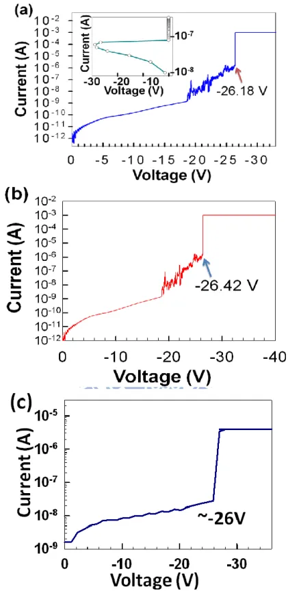
Figure3.5 I-V characteristics of forming process on the (a) Ti/TiN/SiO2/FeOx/Fe/Pt
and (b) Ti/TiN/SiO2/FeOx/FePt structures for V-sweep measurement. In
addition, the inset of (a) also shows the I-V characteristics of the forming process for I-sweep measurement. Fig. (c) shows the forming process of the Pt/SiO2/Pt structure. ---
---
-p.58Figure3.6 Linear fitting results of log-log scale in (a) negative voltage region and (b) positive voltage region for the Ti/TiN/SiO2/FeOx/FePt structure. The
insets of (a) and (b) show a plot of current vs temperature and a plot of ln(I/V) vs V1/2 at voltage higher than +2.8 V in HRS, respectively. The arrows indicate voltage sweeping directions. ---
---
---p.59states for a Ti/TiN/SiO2/FeOx/FePt structure. --
---
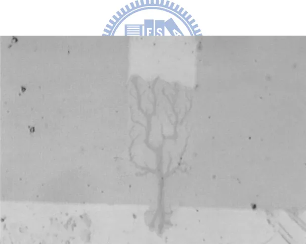
---p.59Figure3.8 OM images of a Ti/TiN electrode surface (a) before and (b) after a higher voltage stress biasing. ---
---
-p.60 Figure3.9 SEM images of the Ti/TiN electrode surface after (a) negative stress and(b) positive stress conditions. ---
---
---p.60 Figure3.10 AFM image of the sample with a dark pit after stripping the top electrodeby wet chemical etching. ---p.61
Figure3.11 Fe 2p3/2 XPS spectra near the interface region of the SiO2/(FeOx)/FePt
structure after a positive and a negative bias stress contidions. Fe 2p3/2
features for metallic Fe at 707.3 eV, FeO at 709.8 eV, Fe3O4 at 710.4 eV
and Fe2O3 at 711.4 eV were assigned. ---
---
---p.62Figure3.12 Schematic pictures of the electromigration of O2- in a sandwiched
structure of Ti/TiN/SiO2/FeOx/Fe-contained electrode during (a) negative
stress and (b) positive stress conditions. ---
---
---p.63 Figure3.13 Proposed switching model of the Fe-electrode-contained RRAM structure for (a) an initial state to a formed state, (b) a “set” state to a “reset” state, and (c) a“reset” state to a “set” state. ------
-p.64 Figure3.14 Comparison of 50-cycle bipolar switching behaviors between the (a) Ti/TiN/SiO2/FeOx/FePt and (b) the Ti/TiN/SiO2/FeOx/Fe/Pt structures.---
---
--p.65 Figure3.15 Statistical comparison of (a) set/reset voltages, (a) set/reset current, and (c)Figure3.16 Comparison of AES depth profiles of Fe and O between a SiO2/FePt and a
SiO2/Fe/Pt stacked layers. ---
---
-p.67Figure3.17 Electrical retention characteristics of the (a) Ti/TiN/SiO2/FeOx/Fe/Pt and
(b) the Ti/TiN/SiO2/FeOx/FePt structures. ---
---
p.68Figure3.18 Illustrations of the annealed Ti/TiN/SiO2/FeOx/FePt device structures and
their process flows. ---
---
p.80Figure3.19 Illustrations of the annealed Ti/TiN/SiO2/FeOx/Fe/Pt device structures and
their process flows. ---
---
---p.80Figure3.20 Cross-sectional TEM of the Ti/TiN/SiO2/FeOx/FePt structures (a) without
(as-deposited condition) and with a thermal treatment of (b) RTA-30 sec, (c) RTA-60 sec, and (d) FA-30 min at 600 ℃. ---
---
---p.81Figure3.21 XRD θ -2θ scan results for the TiN/SiO2/FeOx/FePt structures without
(as-deposited condition) and with a thermal treatment of RTA-60 sec, and FA-30 min at 600 ℃. Symbol (◆) indicates the additional diffraction peaks appeared only in the thermal-treated samples and contributed from the crystallinity of FeOx phases. ---
---
--p.83Figure3.22 XPS depth profiles of Fe-2p on the SiO2/FeOx/FePt structures (a) without
(as-deposited condition) and with a thermal treatment of (b) RTA-60 sec and (c) FA-30 min at 600 ℃. The depth profiles are obtained by an Ar sputter etching in the SiO2 layer, collecting the XPS data at various depths.
The etching times of the spectra are from bottom to top 300, 320, 340, and 360 sec. --
---
---p.84structures (a) without (as-deposited condition) and with a thermal treatment of (b) RTA-30 sec, (c) RTA-60 sec, and (d) FA-30 min at 600
℃ .
---
---
---p.85Figure3.24 All I-V comparisons of the Ti/TiN/SiO2/FeOx/FePt structure with different
thermal-treated conditions
.
-----
---p.87 Figure3.25 Statistical comparisons of (a) set voltage, (b) set current, and (c) set powerfor the different thermal-treated Ti/TiN/SiO2/FeOx/FePt structures. ---p.88
Figure3.26 Statistical comparisons of (a) reset voltage, (b) reset current, and (c) reset power for the different thermal-treated Ti/TiN/SiO2/FeOx/FePt structures.
---
---
---p.89Figure3.27 Room-temperature retention comparisons of the Ti/TiN/SiO2/FeOx/FePt
structures without (as-deposited condition) and with a thermal treatment of RTA-60 sec and FA-30 min at 600 ℃. --
---
-p.90Figure3.28 85 ℃ retention comparisons of the Ti/TiN/SiO2/FeOx/FePt structures
without (as-deposited condition) and with a thermal treatment of RTA-60 sec and FA-30 min at 600 ℃. ----
---
----p.90Figure3.29 50-cycle bipolar switching behaviors of the Ti/TiN/SiO2/FeOx/Fe/Pt
structures (a) without (as-deposited condition) and with a thermal treatment of (b) RTA-30 sec, (c) RTA-60 sec, and (d) FA-30 min at 600 ℃. ---
---
---p.91Figure3.31 Statistical comparisons of (a) set voltage, (b) set current, and (c) set power for the different thermal-treated Ti/TiN/SiO2/FeOx/Fe/Pt structures. ---p.94
Figure3.32 Statistical comparisons of (a) reset voltage, (b) reset current, and (c) reset power for the different thermal-treated Ti/TiN/SiO2/FeOx/Fe/Pt structures.
---
---
-p.102 Figure3.33 Continuous bipolar switching behaviors of the 600 ℃-60 sec treatedTi/TiN/SiO2/FeOx/Fe/Pt structure under a series of compliance current
limitations. ---
---
---p.103 Figure3.34 Statistics of (a) On current, (b) Off current, and (c) On/Off current ratio for the 600 ℃ -60sec treated Ti/TiN/SiO2/FeOx/Fe/Pt structure withcompliance currents. --
---
---p.103 Figure3.35 Statistics of (a) reset current, (b) reset current, and (c) reset power for the 600 ℃-60 sec treated Ti/TiN/SiO2/FeOx/Fe/Pt structure with compliancecurrents. ----
---
----p.104 Figure3.36 Statistics of (a) set voltage, (b) set current and (c) set power for the 600℃ -60 sec treated Ti/TiN/SiO2/FeOx/Fe/Pt structure with compliance
currents. ---
---
--p.105 Figure3.37 Continuous bipolar switching behaviors of the 600 ℃-60 sec treatedTi/TiN/SiO2/FeOx/Fe/Pt structure under a series of stopping voltage in
reset region. ---
---
---p.106 Figure3.38 Statistics of (a) On current, (b) Off current, and (c) On/Off current ratiofor the 600 ℃ -60 sec treated Ti/TiN/SiO2/FeOx/Fe/Pt structure with
Figure3.39 Statistics of (a) set voltage, (b) set current and (c) set power for the 600 ℃-60 sec treated Ti/TiN/SiO2/FeOx/Fe/Pt structure with different stopping
voltages in the reset region. -
---
---p.108 Figure3.40 Statistics of (a) reset voltage, (b) reset current and (c) reset power for the 600 ℃-60 sec treated Ti/TiN/SiO2/FeOx/Fe/Pt structure with differentstopping voltages in the reset region. ----
---
----p.109Appendix
Figure Captions
FigureA.1 Illustration of the proposed titanium oxinitride nanocrystals device structure and process flows. ---
---
---p.133FigureA.2 Cross-sectional TEM of the Ti-SiO2 co-sputtered samples with the different
annealing temperatures of (a) 500 ℃, (b) 700 ℃, and (c) 900 ℃ in N2
ambient for 1 min. A schematic diagram of device structure was also shown in the inset of Fig. 1(a). ---
---
--p.134FigureA.3 Comparisons of XPS for (a) O-1s, (b) N-1s, and (c) Ti-2p on the Ti-SiO2
co-sputtered samples with different annealing treatments of 500 ℃, 700 ℃, and 900 ℃ in N2 ambient. ---
---
--p.135FigureA.4 C-V characteristics of different gate voltage sweeping regions on the Ti-SiO2 co-sputtered samples with the annealing treatments of (a) 500 ℃,
(b) 700 ℃, and (c) 900 ℃ in N2 ambient. The arrows indicate voltage
sweeping directions. ---
---
---p.138FigureA.5 Charge loss characteristic of the TiNxOy NCs capacitor with the annealing
with germanium doping and process flows. --
---
---p.148FigureA.7 Cross-sectional TEM of the 10-nm-pre-capped samples with the annealing treatments of (a) 400 ºC, (b) 500 ºC, and (c) 600 ºC as well as the 20-nm-pre-capped sample with the annealing treatment of (d) 600 ºC.-p.149
FigureA.8 XPS spectra of the 10-nm-pre-capped samples with the annealing conditions of 400 ℃, 500℃, and 600 ℃ for (a) O-1s, (b) Si-2p, (c)Ti-2p as well as the 20-nm-pre-capped sample for (d) Ge-2p. FigA.8 (e) shows a comparison on overall region XPS spectra between the Ti-based germanosilicide samples annealed at 500 and 600 °C. ---
---
---p.151FigureA.9 A comparison of high frequency C-V characteristics on the 10-nm-pre-capped samples with the annealing treatment of (a) 400 ºC, (b) 500 ºC, and (c) 600 ºC as well as the 20-nm-pre-capped sample with the annealing treatment of (d) 600 ºC. ---
---
--p.154FigureA.10 A comparison of retention characteristics between the 10-nm-pre-capped sample annealed at 500 ºC and the 20-nm-pre-capped one annealed at 600 ºC. ---
---
p.156Table Captions
Table 3-1 Comparison of the mean value of Set & Reset voltage, Set & Reset current and Set & Reset power between the FePt-contained structure and the Fe-contained one.
---
67 Table 3-2 Comparison of the mean value of Set & Reset voltage, Set & Reset current,Set & Reset power and forming voltage of the Ti/TiN/SiO2/FeOx/FePt
Chapter 1
Introduction
1.1 Overview of Nonvolatile Memory
In 1960’s, due to the high cost, large volume, and high power consumption of the magnetic-core memory, the electronic industries urgently needed a new kind of
memory device to replace the magnetic-core memory. In 1967, D. Kahng and S. M.
Sze invented the floating-gate (FG) nonvolatile semiconductor memory at Bell Labs
[1.1]. Because of exhibiting several advantages, such as fast read access time, better
kinetic shock resistance than hard disk and, most importantly, compatibility with the
current complementary-metal-oxide-semiconductor (CMOS) process, the stacked-gate
FG device structure, as shown in Fig. 1-1, becomes the mainstream nonvolatile
memory (NVM) device in last few decades and is widely used in both standalone and
embedded memories.
The basic operation of a FG device is that charges are injected from the silicon
substrate across the tunneling oxide and stored in the floating gate by applying an
appropriate gate voltage. Then, the stored charges can cause a threshold-voltage shift,
and the device is at a high-threshold state (programmed). For a well-designed memory
so-called Flash memory, which has a byte-selectable write operation combined with a sector ―flash‖ erase, and has created a huge industry of portable electronic systems, such as MP3 player, PDA, Notebook, and flash driver. Besides, the flash memory can
be further classified into two types, NOR and NAND flash memories, according to
their functions and advantages [1.2]. NOR Flash offers faster read speed and random
access capabilities, making it suitable for code storage in devices such as PDA and
cell phone. In contrast to NOR flash, the NAND memory, which offers faster
write/erase capability and higher density is typically used for storing large quantities
of data.
In spite of such a huge commercial success, conventional FG devices have their
limitations. The most prominent one is the issue on scaling down of the tunnel oxide.
According to the 2007 International Technology Roadmap for Semiconductors (ITRS)
flash memory [1.3], tunnel oxide thickness must be more than 6-nm to assure enough
retention time, as shown in Fig. 1-2. This basic limitation on tunnel oxide leads to a
high programming/erasing voltage and low operation speed for the device. If tunnel
oxide were scaling to below 2-nm, the programming/erasing voltage could be reduced
to smaller than 4V. Although the thin tunnel oxide can effectively enhance the
programming/erasing speed and reduce operation voltage, the thick oxide is required
generate in tunnel oxide, which might induce a leak path in the tunnel oxide and
results in the stored charge loss. These difficult trade-off problems hinder the scaling.
To overcome the scaling limits of the conventional FG structure, not only the
charge based storage technology, such as nanocrystal NVM devices [Appendix], but
also the non-charge based storage technology is researched to be the candidates for
the next generation of NVMs, such as phase-change memory (PCM),
magnetoresistive random access memory (MRAM), and resistive random-access
memory (RRAM), exhibiting the reproducible changes of electrical resistance.
RRAM, especially, has the potential to become the front runner among other
non-volatile memories. Compared to PRAM, RRAM operates at a faster timescale
(switching time can be less than 10 ns), while compared to MRAM, it has a simpler,
smaller cell structure (less than 8F² MIM stack). Compared to flash memory and
racetrack memory, a lower voltage is sufficient and hence it can be used in low power
applications. Moreover, ITRI has recently shown that RRAM is scalable below 30 nm.
It is believed that if a filament is responsible, it would not exhibit direct scaling with
cell size.
the next generation nonvolatile memory devices. RRAMs use of the resistance
changes as different memory states. By electrical field or current effects, the
conductivity could be switched between high and low resistance reproducibly, so such
the bistable resistance states could be represented to different digital states as a
memory device. The advantages of RRAM are with high cell density array, high
operation speed, low power consumption, high endurance and lower scale limit.
Moreover, RRAMs have the features of nonvolatility, long retention time, and
non-destructive readout.
The basic structure for RRAM is made up of only metal-insulator-metal (M-I-M),
which could be further integrated into 1D1R (a diode and a resistor) or 1T1R (a
transistor and a resistor) structures [1.4-1.5]. The top and bottom electrodes could be
made by metals or conducting transition metal oxides [1.4], the choice of which
would impact on the resistive switching properties because of their different
crystallinities, work functions and ability of oxygen gettering [1.6-1.8]. On the other
hand, the main character of resistive switching is the insulator layer sandwiched
between the electrodes. The insulator for the M-I-M structure may be not really
insulating, but also semiconducting, depending on its composition and stoichiometry
[1.9]. The insulator would be called ―resistance switching layer‖ in the following
also affects the resistive switching characteristics [1.10].
Resistive switching phenomena have been discovered in many materials and now
the research mainstream is concentrated on groups of binary oxides, such as TiO2
[1.11], ZrO2 [1.12], NiO [1.13], Al2O3 [1.14], CuxO [1.15], Fe2O3 [1.16], ZnO [1.17],
HfO2 [1.8], SiO2 [1.18, 1.19] and MoOx [1.20], perovskite oxides, such as Cr-doped
SrTiO3 [1.10], Cr-doped SrZrO3 [1.21], and Pr0.7Ca0.3MnO3 [1.22], manganites, and
organic/polymers. Of note, the binary oxides adopted in RRAM application are
candidates or have been widely used in other field of CMOS devices. Thus, the
compatibility with modern CMOS process would not be a serious issue. Moreover,
these binary oxides have such simple element components that it could be easier to
control the proportion of metal and oxygen composition.
1.2 Motivation
As mentioned above, because of facing the scaling limits of the conventional FG
structure, works on researching the most probable candidate for the next generation of
NVMs are studied in this dissertation, i.e. non-charge based storage structure. For
non-charge storage structure, resistive switching effects on a thin FeOx transition layer
reaction between nonstoichiometric compounds of iron oxides, which takes place
locally near the electrode region. In addition, because of the ease of oxidation of iron
atoms, we provided a method to produce a nonstoichiometric FeOx layer, the critical
resistance switching layer, near the electrode region simply for RRAM applications
by depositing a plasma-enhanced tetraethyl orthosilicate oxide onto the Fe-contented
electrode to form a SiO2/FeOx/ Fe-contented electrode structure. Moreover, thermal
annealing effects and multi-level effects of such a FeOx transition layer are also
studied at the same time.
1.3 Organization of the dissertation
This dissertation is divided into four chapters. The contents in each chapter are
described as follows.
In chapter 1, general background of resistive switching nonvolatile memory
devices is introduced.
In chapter 2, operation method of resistive switching nonvolatile memory
devices is briefly described as well as their basic physical characteristic and
mechanism. Furthermore, reliability discussions are also mentioned in this chapter.
In chapter 3, memory characteristic researches on thin-FeOx-contained resistive
oxide/iron transition region by a Fe-contented-electrode of an Metal-Insulator-Metal
structure, i.e. a sandwiched TiN/SiO2/Fe/Pt or TiN/SiO2/FePt structures, are studied,
including three main sections: (a) Basic characteristics to demonstrate resistive
switching effects on a thin FeOx transition layer produced at the interface of SiO2/Fe
and SiO2/FePt structures, including resistive switching properties, insulator thickness
effects, area size effects, and bubble effects; (b) Thermal annealing effects to
demonstrate improvements of resistance switching characteristics in a thin
FeOx-transition-contained structure as well as the mechanism by discussing the
reliability and statistic characteristics; and (c) Multi-level effects to demonstrate
tunable resistance switching characteristics in a thin FeOx-transition layer by
controlling sweeping voltage and compliance current.
Finally, the summarization of all experimental results in this dissertation and the
suggestions for the future work are presented in chapter 4.
Besides, in the appendix, memory characteristic researches on titanium-based
nanocrystal nonvolatile memories, titanium oxinitride nanocrystals synthesized via
nitridizing titanium oxide, are demonstrated, including formation, composition, and
electric properties. In addition, research on lowering the synthesis temperature of
Fig. 1-1 Structure of a conventional floating-gate nonvolatile memory device. The floating-gate device is constructed by the MOSFET device with a modified gate stack (tunnel oxide/floating gate/blocking oxide/gate electrode), where the floating gate is fabricated by an electronically continuous poly-silicon layer and is employed as the charge storage media.
Chapter 2
Basic Principles of Nonvolatile Resistive Switching
Memory
2.1 Material Sources of Resistive Switching Memory
Resistance switching in metal-insulator-metal (M-I-M) structures has been a long
standing problem in materials and device physics for 40 years. To date, many
materials with resistance switching characteristics have been widely demonstrated,
which could be simply grouped into perovskite oxides, such as Cr-doped SrTiO3 [2.1],
Cr-doped SrZrO3 [2.2], and Pr0.7Ca0.3MnO3(PCMO)[2.3] La1-XCaXMnO3 (LCMO),
transition metal oxides, such as FeOx [2.4], ZrOx [2.5], TiO2 [2.6], NiO [2.7] , CuxO
[2.8], HfO2 [2.9] and (Pr,Ca)MnO3 [2.10], organic polymer materials [2.11],
solid-state electrolyte (programmable metallization cell), such as Cu:SiO2, Ag:TiO2,
Cu:Ta2O5, Ag:CuS, and Ag:GeSe, rare-earth metal oxide, such as Gd2O3 [2.12], CeO2
[2.13] and even SiO2 [2.14], Al2O3 [2.15]. However, the resistance switching
mechanisms are not well understood and identified yet. Therefore, more and more
researches on resistance switching are still investigated recently.
current-voltage operation characteristic of an initial-stated (as-prepared sample)
resistive switching memory for (1) forming, (2) reset, and (3) set processes [2.16,
2.35]. It is found that after the forming process, which is required to initiate the
resistive switching properties of oxide films, a basic writing/erasing operation (or
named set/reset process) of bistable resistive switching in one cell could be achieved
by DC sweeping or pulse modes. First, if the resistance state of a RRAM cell is held
in a high resistance state (HRS), the current of the cell would increase during DC bias
sweeping over a threshold voltage (or a switching voltage). Then, the resistance
exchanges from the HRS to a low resistance state (LRS), which is defined as a
process of ―set‖. Furthermore, when DC bias sweeps again, the LRS would switch
back to a HRS, associated with an enormously current drop after a switching voltage.
Then, the resistance exchanges from the LRS to a HRS again, which is defined as a
process of ―reset‖. On the other hand, for reading operation, the bias should not
exceed the switching voltage to keep the expected ―set‖ or ―reset‖, preventing the
memory state from variation.
Details of forming voltage, unipolar, bipolar characteristics and even circuit
realization will discuss in the next sections. Of note, in order to unify the operation
parameters in the following text, the ―set‖ and ―reset‖ would be used to describe the
set voltage, reset voltage, the resistance at low resistance state (LRS) and the
resistance at high resistance state (HRS), respectively. The Vset and Vreset represent the
voltage where set and reset processes begin to occur, and RLRS and RHRS were
measured at V = 0.2 V for LRS and HRS, respectively.
2.2.1 Forming Process
Before the resistive switching characteristics are observed to exhibit, a ―forming process‖ or a ―conditioning process‖ is necessary to activate the resistive memory devices, i.e. the first transition of resistive switching materials from highly insulating
to a more conductive state. The forming process needs a high-voltage stress (Vforming)
applied on the pristine device to change the local microstructure or morphology of the
RRAM device and form the conduction paths (also named inner conducting
filaments), which is equivalent to dielectric breakdown reported by Kinoshita et al.,
between top and bottom electrodes. For short, the forming process is similar to soft
breakdown, leading to the conducting paths (filaments) composed of clusters of point
defects as shown in figure 2-2 [2.18] and figure 2-3 [2.19]. The stoichiometry and the
thickness of the resistive memory film have been reported to have influences on
oxygen vacancies, or anode material to modify the anode region or the whole memory
device. It should also be noted that both the polarity of the forming voltage seems to
induce a LRS for the unipolar device, which was considered as typical soft breakdown
of the insulator. However, for the bipolar device, it was reported by by J Joshua Yang,
et al. that the electric field polarity repels the growing vacancy channels from
touching the top electrode—the Schottky-like barrier is not heavily reduced after
forming and the post-forming state is OFF. In other words, the conducting channel
penetrates the bulk film but not the Schottky-like interface region [2.35]. Therefore,
the forming process could induce the bipolar device to either a LRS or a HRS,
depending on which side the interface barrier is.
2.2.2 Unipolar (or Nonpolar)
Figure 2-4 shows a typical unipolar I-V plot under DC sweep operation. Unipolar
means the operation of switching is independent on the polarity of the voltage and
current signal. In unipolar system, the low-resistance state (ON state) is switched (―turn OFF‖) into the high-resistance state (OFF state) by sweeping to over a reset voltage, which needs to be below the set voltage and with the compliance current
condition (1 → 2 or 1’ → 2’). On the other hand, the unipolar system in its
state (ON state) by sweeping to over a set voltage (3→4 or 3’→4’). It should be noted
that this operation requiring same voltage polarities to switch, whether positive
on/positive off or negative off/negative on. Because we could switch device resistance
with the same or reversed voltage polarity in unipolar resistive switching, therefore
the unipolar switching is also called nonpolar resistive switching. The unipolar
resistive switching is thought to be the fuse/antifuse of conduction paths or filaments.
The unipolar switching usually has much larger resistance change than the bipolar
switching, and this makes it much easier to read the memory state. In addition,
devices using unipolar switching can be potentially integrated in higher density. This
type of switching behavior has been observed in many highly insulating oxides, such
as binary metal oxides.
2.2.3 Bipolar
Figure 2-5 shows a typical bipolar I-V plot under DC sweep operation. Bipolar
means the operation of the set to the ON state occurs at one voltage polarity, and the
reset to the OFF state take place on reversed voltage polarity, i.e. this operation
requiring different voltage polarities to switch, whether negative on/positive off or
voltage sweeping to over a reset voltage (1→2→3). On the other hand, the bipolar
system in its high-resistance state (OFF state) is switched (―turn ON‖) into the
low-resistance state (ON state) by a positive voltage sweeping to over the set voltage
(4→5→6). The mechanism of bipolar resistive switching is considered to be the
migration of anions. This type of resistive switching behavior occurs with many
semiconducting oxides, such as complex perovskite oxides.
2.2.4 Circuit Realization
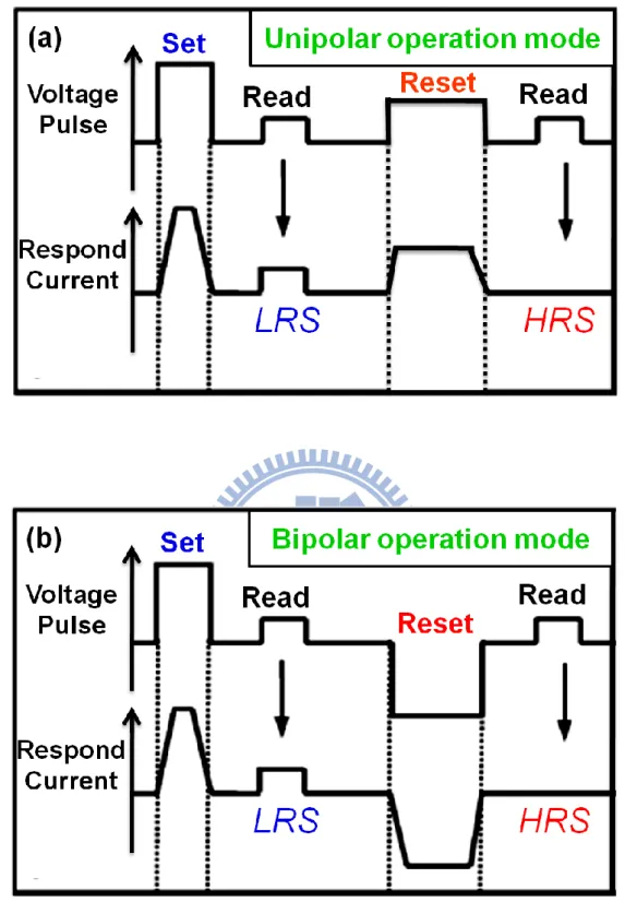
In the real circuits, it is the pulse mode switching that is the practical operation
method due to fast operation speed and lower power consumption. Ideally, operation
sequences of set/reset voltage pulses and the corresponding respondent current for
unipolar and bipolar switching are schematically shown in figure 2-6(a) and (b),
respectively [2.22]. For example, the waveforms of set and reset process to operate a
RRAM device were demonstrated in figure 2-7(a) and (b), respectively [2.7]. The
other example is also shown in figure 2-8 [2.23]. The pulse heights and widths for set
and reset must take a balance. The larger the pulse height is, the shorter the pulse
width is needed. The reading pulses with small pulse heights are also designed in
order not to vary the memory states.
in figure 2-9, which contains the word lines crossed with the bit lines. For realization
applications, the 1D1R (1 diode and 1 resistor) or the 1T1R (1 transistor and 1 resistor)
structure must be used to prevent misreading as shown in figure 2-10 and figure 2-11,
respectively. I. G. Baek et al. [2.7] reported that if a cell is in high resistance state and
its neighboring cells are in low resistance state, it will be misread as low resistance
state due to the leakage current path around its neighboring cells as shown in figure
2-12 [2.24]. Hence, a rectifying element is required for each cell in an array to limit
the current paths. The minimum sizes for the 1D1R and the 1T1R structures are 4F2
and 6F2 respectively, and these structures would meet the requirement for high density
arrays.
2.3 Basic Conducting mechanisms of Resistive Switching Memory
Based on conductivity, transition metal oxides could be insulator, semiconductor
or metal depending on the composition of the oxide materials. Hence the conducting
mechanisms may vary because of their different physics and chemistry characteristics.
The most discussed materials in RRAM application generally belong to insulator or
semiconductor according to the constitution and stoichiometry, and the electron
current fitting procedure would give insight into the conduction mechanisms.
2.3.1 Ohmic conduction
Ohmic conduction takes place when the injected carrier density is far less than
the thermally-generated carrier density. Generally, it applies to the condition of low
electric field region in which thermally-generated carriers are dominant in conduction.
The current-voltage characteristics follow Ohm’s law that the current passing through
a resistor from one terminal to the other is proportional to the voltage drop across the
two points. In addition, the temperature effect is also described in Ohmic conduction
behavior. Due to the electron and phonon scattering effects, the conductivity rises
with increasing temperature for conduction in semiconductor, while with decreasing
temperature for metal conduction. The following is the expression for Ohmic
conduction: e x p -c J a V T
where a (and c) is constant, and V is the applied voltage.
2.3.2 Space charge limited current
The mechanism of space charge limited current (SCLC) is attributed to defects
injection from an electrode, the space charge may form if the charge carriers are
trapped and distributed over a region of area without being neutralized. The further
flow of charge carriers would be impeded by this space charge region. It should be
noted that the injected carriers are mostly electrons. As for conductive media, the
trapped carriers are able to be neutralized or screened rapidly; therefore the space
charge region would not form.
The complete trapped controlled SCLC mechanism is composed of two stages
[2.6], trap-unfilled SCLC and trap-filled SCLC, both can be written as the following
expression: 2 0 3 9 1 8 r V J L
where J is the current density, is the ratio of free electron to trapped electron, NC is
the effective density of states in the conductive band, Nt is the number of emptied
electron traps, is the permittivity of free space, r is the static dielectric constant,
is the electron mobility, V is the applied voltage and L is the film thickness. At first
stage, the traps are not filled with charges and the formula can be rewritten with <<1
as the following: 2 0 3 9 8 r V J L
2 0 3 9 8 r V J L 2.3.3 Schottky emission
Schottky emission is mainly attributed to the Schottky contact of the
metal-insulator interface. For the carriers to transport, they must jump across the
barrier height of one of the interfaces, travel through the dielectric film, and
eventually reach the other side. It is the thermionic emission that enables the carriers
(mostly electrons) to overcome the interface barrier height. Therefore temperature is
the key factor that energetic carriers (hot carriers) are easier to jump across the barrier.
The formula of Schottky emission is expressed as below:
0 2 - ( - / 4 e x p q b qV r d J A T kT
where A* denotes Richardson constant, b is the Schottky barrier height, is the
permittivity of free space, r is the dynamic dielectric constant, V is the external
applied voltage and d is the insulator thickness.
2.3.4 Frenkel-Poole emission
Frenkel-Poole emission is pretty much similar to Schottky emission mechanism.
The main differences are that Frenkel-Poole emission describes the process for
material, and the barrier lowering is twice as large as that in Schottky emission
mechanism. Temperature is also crucial for this carrier transportation process, while
electric field plays a more important role in this mechanism than in Schottky emission,
which suggests that field effects have greater impact on defect-related behavior. The
current-voltage relationship can be written as the following formula:
0 - ( - / 4 exp q t qV r d J BV kT
where B is a material-related constant, t is the trap level, and other parameters are
the same as those in Schottky emission.
2.3.5 Tunneling
Tunneling is the most common conduction mechanism through insulators under
high fields. The tunnel emission is a result of quantum mechanism by which the
electron wave function can penetrate through a potential barrier. It has the strongest
dependence on applied voltage but is essentially independent of the temperature.
Tunneling mechanism can be divided into direct tunneling and Fowler-Nordheim
tunneling where carrier tunnel through a partial width of the barrier. The
current-voltage relationship can be written as the following formula:
) b -exp( V ) (q 2m 4 -exp J 2 2 3 B * 2
where i is the electric field in insulator, m* is the effective mass, B is the berrier
height, and V is the applied voltage.
2.4 Switching Characteristics and Models of Resistive Switching
Memory
The major possible models having been proposed by other research groups are
sorted partially as two parts, one is filament-type resistance switching and the other is
interface-type resistance switching [2.16]. The two models may be applied for some
combinations of electrodes and oxide materials. However, these models are mainly
derived by indirect observation or electrical measurements, but the switching
mechanisms are not still well known because of having less direct and striking
evidences to prove.
2.4.1 Filament-type resistive switching
The filament-type model comes from the nature of oxide breakdown and
integrity that defects existing in an oxide bulk, such as the interstitials, oxygen
vacancies and metals constitute the leakage current path, indicated in figure 2-13 [2.
25]. This model has been proposed since 1970’s and is one of the earliest models in
have obtained a lot of attention, the further and more detailed studies have been
realized to investigate the possible mechanisms. Among these proposed models, it is
almost the filament-type model that prevails in many of binary oxide films, such as
TiO2 [2.6], ZrO2 [2.5], NiO [2.7] and CuxO [2.8] and even in solid electrolyte, such as
Ag-Ge-S shown in figure 2-14 [2.28]. The most obvious evidences for the
filament-type model are conductive atomic force microscopy (CAFM) mapping
results at low resistance state. C-AFM is one of the power tools to study the local
conductivity throughout the film. B. J. Choi et. al. and J. Y. Son et. al. reported that by
scanning the film surface with CAFM, only several conductive points exist and
account for the current conduction, as shown in figure 2-15 [2.29] and figure 2-16
[2.30]. Fortunately, K. Fujiwara et. al. reported the observation of the a filamentary
conducting path in a CuO film between Pt electrodes by Scanning electron
microscope as shown in figure 2-17, providing the experimental reality of the
conducting filament for the filament-type model [2.31]. Generally, the switching
transformation of the filament-type model between the LRS and HRS is naively
considered to be an abrupt transformation, causing the correspondence of
abrupt-changed current from LRS (or HRS) and HRS (or LRS) during the voltage
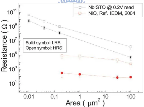
As shown in figure 2-18, the resistance of NiO memory cells is almost independent of
the area, suggesting that resistive switching is a local phenomenon, i.e. the
filament-type phenomenon [2.32].
2.4.2 Interface-type resistance switching
The interface-type resistance switching model is wide-spreading especially in the
material system of PCMO [2.33] and Nb;STO [2.34]. This model can be further
classified into two types in accordance with the type of semiconductor, the n-type
semiconductor and p-type semiconductor. As shown in figure 2-19 [2.16], when the
number of oxygen vacancies in the oxide layers is reduced, the Ti/PCMO/SRO cells
converted to a LRS and the SRO/Nb:STO/Ag cells converted into a HRS. It is
because that in p-type oxide semiconductors, oxygen vacancies are considered to be
an acceptor scavenger. Therefore, the reduction in oxygen vacancies at the interfaces
upon annealing may cause the depletion layer to become narrower in PCMO,
resulting in a decrease in the contact resistance. On the other hand, since an oxygen
vacancy acts as an effective donor in n-type oxide semiconductors, the reduction in
the number of oxygen vacancies may cause the depletion layer to become wider in
Nb:STO, resulting in an increase in the contact resistance. For example, the schematic
Generally, the switching transformation of the interface-type resistance switching
model between the LRS and HRS is also naively considered to be an smooth and
gradual transformation, causing the correspondence of gradual-changed current from
LRS (or HRS) and HRS (or LRS) during the voltage sweeping. Moreover, the
interface-type resistance switching model could also be affirmed by the dependent
electrode area relationship to resistance values (both the HRS and LRS). As shown in
figure 2-18, the resistance of Nb-doped SrTiO3 memory cells depends linearly on the
area, suggesting that the resistive switching takes place over the entire area of the
interface, i.e. the interface-type resistance switching phenomenon.
2.5 Reliability: Retention and Endurance
Unlike to logic IC, nonvolatile memory is more concerned with reliability than
performance. The reliability includes two parts, retention and endurance. Both
reliability tests are very important for nonvolatile memory application in the portable
electronic productions market and they are also a kind of specifications to define the
charge loss phenomena during a long-term usage. In general, nonvolatile memory
must be able to bear 100K-1M program/erase operation cycles (endurance), and can
chemical reactions, such as redox between nonstoichiometric compounds, diffusion of
ions, and phase change of materials, deviation of the operation voltage and variation
of high and low resistance state values are the most concerned reliability issues for a
RRAM device. Moreover, different materials could exhibit different resistive
switching mechanisms. To date, therefore, RRAM reliability could be discussed case
by case, depending on what kind of material and mechanism it is. In general, there are
still some required specifications for nonvolatile memory applications introduced as
following:
(a) Retention
For nonvolatile memory, the data information must be conserved over than ten
years. This means that the charge loss rate have to be as low as possible. One possible
origin of charge loss is through the degradation of the film materials, which may be
responsible for time and temperature dependent on retention behavior of nonvolatile
memory devices. The retention capability of nonvolatile memories are usually
examined by using accelerated tests that usually adopt screening electric fields and
hostile environments at high temperature.
Endurance is a number of erase/write operations. Generally speaking, Flash
products are specified for 106 erase/program cycles. Nevertheless, the endurance
requirement may be relaxed with the increase of memory density for the other
applications. The endurance requirement is relaxed to 100K cycles for 256 MB
memory. In the higher density, a certain cell in a block has less possibility to be
written and erased since the memory operation on the cell is repeated after using up
the whole memory blocks. The endurance requirement is sufficient for the user to take
Fig. 2-1(a) A typical unipolar current-voltage operation characteristic of an initial-stated (as-prepared sample) resistive switching memory for (1) forming, (2) reset, and (3) set processes. [2.16]
Fig. 2-1(b) A typical bipolar current-voltage operation characteristic of an initial-stated (as-prepared sample) resistive switching memory for (1) forming, (2) reset, and (3) set processes. [2.35]
Fig. 2-2 Schematics of an initial state (as-prepared sample) and a formed state after the forming process. [2.16]
Fig. 2-3 Optical image from the filamentary region. This is a typical breakdown filament. [2.17]
Fig. 2-4 Typical unipolar I-V curves of RRAM switching in voltage sweeping mode [2.16].
Fig. 2-5 Typical bipolar I-V curves of RRAM switching in voltage sweeping mode. [2.16].
Fig. 2-6 Schematic operation sequences of set/reset voltage pulses and the corresponding respondent current for (a) unipolar and (b) bipolar switching. [2.22]
Fig. 2-7 Switching dynamics monitored with programming and reading pulses. Pulse waveforms and transition for (a) set process and (b) reset process [2.7].
Fig. 2-8 (a) Characteristic 0.4 V monitoring pulses with the programming pulse in between (black line), and switching from HRS to LRS induced by a single 1.5 V pulse with a 10 ns duration (red line). (b) Switching from LRS to HRS driven by a single reset 1 V pulse with a 10 ns duration. [2.23]
Fig. 2-10 Conceptual schematic cell unit composed of 1D1R structure [2.7].
Fig. 2-11 Cross-sectional schematic and basic circuit diagram of cell unit composed of 1T1R structure [2.18].
Fig. 2-12 (a) Generalized cross-point structure with memory and switching elements. (b) Reading interference without switch elements. (c) Rectified reading operation with
Fig. 2-13 Schematic of the filament in an oxide [2.16, 2.25].
Fig. 2-14 Schematic of (a) the initial formation of a conductive filament, and (b) radial growth of the CF. Both stages of the programming operation are driven by electrochemical reactions at the electrodes and ion migration. [2.28]
Fig. 2-15 Conductivity mapping results of the (a) low resistance and (b) high resistance state TiO2 films, using conductive AFM (CAFM). The bright spots
represent the conducting points [2.29].
Fig. 2-16 (a) The CAFM image of the NiO thin film for the Roff state corresponding to 100 switching cycles. The bias voltage of 0.1 V was used for the CAFM measurement. (b) The CAFM image of the NiO thin film for the Ron state
Fig. 2-17 Illustration of a filamentary conducting path in a lateral planar configuration. (b) Scanning electron microscope image of a filamentary conducting path in a CuO film between Pt electrodes. (2.31)
Fig. 2-18 5 Area dependence of resistance values in high and low resistance states for Nb-doped SrTiO3 (Nb:STO) and NiO memory cells. The resistance of Nb:STO
memory cells depends linearly on the area, suggesting that the resistive switching takes place over the entire area of the interface. The resistance of NiO memory cells is almost independent of the area, suggesting that resistive switching is a local phenomenon. [2.32]
Fig. 2-19 Schematics of the changes in the oxygen vacancy density in the vicinity of the interface. The resistance states of the memory cells are possibly determined by the oxygen vacancy density [2.16].
Fig. 2-20 Band diagram with the conditions of p-type semiconductor for on state (LRS) and off state (HRS), respectively [2.16].
Chapter 3
Characteristics of thin-FeO
x-contained resistive
switching memories
A. Basic Characteristics
3.1 Resistive switching effects on a thin FeO
xtransition layer
produced at the oxide/iron interface of Ti/TiN/SiO
2/Fe-contented
electrode structures
3.1.1 Introduction
Resistance random access memory (RRAM) is one of the most potential
candidates for the next generation of non-volatile memory [3.1] due to its excellent
advantages of high cell density array, high operation speed, low power consumption,
and high endurance [3.2-3.4]. Therefore, there have been many studies of binary
metal oxides with resistance switching characteristics, such as FeOx [3.5], ZrOx [3.6],
TiO2 [3.7], NiO [3.8], Al2O3 [3.9], CuxO [3.10], and HfO2 [3.11] in a
metal-insulator-metal (M-I-M) structure due to, in a word, the inevitable existence of
nonstoichiometry in every oxide thin film [3.12]. Among these insulators, the
switching effect of FeOx was proposed as a redox reaction between
![Fig. 2-5 Typical bipolar I-V curves of RRAM switching in voltage sweeping mode. [2.16]](https://thumb-ap.123doks.com/thumbv2/9libinfo/8257719.171968/49.892.129.791.155.1075/fig-typical-bipolar-curves-rram-switching-voltage-sweeping.webp)
![Fig. 2-7 Switching dynamics monitored with programming and reading pulses. Pulse waveforms and transition for (a) set process and (b) reset process [2.7]](https://thumb-ap.123doks.com/thumbv2/9libinfo/8257719.171968/51.892.138.760.116.420/switching-dynamics-monitored-programming-reading-waveforms-transition-process.webp)
![Fig. 2-11 Cross-sectional schematic and basic circuit diagram of cell unit composed of 1T1R structure [2.18]](https://thumb-ap.123doks.com/thumbv2/9libinfo/8257719.171968/52.892.134.752.372.1042/cross-sectional-schematic-basic-circuit-diagram-composed-structure.webp)

![Fig. 2-20 Band diagram with the conditions of p-type semiconductor for on state (LRS) and off state (HRS), respectively [2.16]](https://thumb-ap.123doks.com/thumbv2/9libinfo/8257719.171968/56.892.149.733.462.1016/fig-band-diagram-conditions-semiconductor-state-state-respectively.webp)