國 立 交 通 大 學
電子工程學系 電子研究所碩士班
碩 士 論 文
在負偏壓溫度不穩定回復時臨界電壓改變量分佈
之統計特性和模式及其時間演繹
Statistical Characterization and Modeling of
Vth
Distribution in NBTI Recovery and Its Time Evolution
研 究 生 :謝泓達
指導教授 :汪大暉 博士
在負偏壓溫度不穩定回復時臨界電壓改變量分佈之
統計特性和模式及其時間演繹
Statistical Characterization and Modeling of
V
thDistribution in NBTI Recovery and Its Time Evolution
研
究 生 : 謝泓達 Student : Hung-Da, Hsieh
指導教授 : 汪大暉 博士 Advisor : Dr. Tahui Wang
國立交通大學
電子工程學系 電子研究所碩士班
碩士論文
A Thesis
Submitted to Department of Electronics Engineering and
Institute of Electronics
College of Electrical and Computer Engineering
National Chiao Tung University
in Partial Fulfillment of the Requirements
for the Degree of
Master of Science
in
Electronic Engineering
July 2012
Hsinchu, Taiwan, Republic of China.
中華民國 一○一 年 七 月
i
在負偏壓溫度不穩定回復時臨界電壓改變量
分佈之統計特性和模式及其時間演繹
學生:謝泓達
指導教授:汪大暉 博士
國立交通大學 電子工程學系 電子研究所
摘要
在本篇論文中,為了了解負偏壓溫度回復時的臨界電壓改變量分佈特 性,我們萃取單一電荷散逸導致臨界電壓改變量,還有單一電荷散逸時 間。我們考慮了活化能(Activation Energy)和缺陷能量(Trap Energy)分 佈 來 模 擬 負 偏 壓 溫 度 (NBT) 操 作 後 的 回 復 (Recovery) 效 應 之 散 逸 時 間 (De-trapping Time)散佈。此外,也研究在經過負偏壓溫度操作後回復時, 單一電荷散逸導致臨界電壓改變量的散佈。我們把這兩個散佈結合到電荷 散逸模型(Trapped Charge Emission Model)。由上述兩個實驗參數來進 行蒙地卡羅模擬經過負偏壓溫度操作後回復的臨界電壓散佈,此結果可精 準符合實驗數據。
ii
Statistical Characterization and Modeling of
V
thDistribution in NBTI Recovery and Its
Time Evolution
Student: Hung-Da Hsieh Advisor: Dr. Tahui Wang
Department of Electronics Engineering &
Institute of Electronics
National Chiao Tung University
Abstract
In this thesis, single charge de-trapping induced threshold voltage shift (vth) and
single charge de-trapping time (e) are extracted to analyze the characteristic of the
threshold voltage (Vth) dispersion in NBTI recovery.
Activation energy (Ea) and trap energy (ET) distributions are investigated to
simulate de-trapping time (e) dispersion during negative bias temperature instability
(NBTI) recovery. Furthermore, single charge de-trapping induced vth dispersion is
investigated during NBTI recovery. A statistical model combining the trapped charge
iii
characterization of the single charge phenomenon, we proposed a Monte Carlo
simulation to simulate the NBTI recovery threshold voltage dispersion. Our model
iv
Acknowledgement
本篇論文之所以能夠完成,首先,我要感謝我的指導教授 ─ 汪大暉 教授,在他嚴謹紮實且耐心研究指導下,使我從中學習到新的知識及正確 的研究態度,在此深表我對老師的感謝。 另外,博士班學長 ─ 小馬學長、榮標學長、岳庭學長、佑亮學長, 碩士班學長 ─ 志宇學長、明瑋學長、書祥學長,帶領我融入實驗室,並 且教導我量測技術和實驗原理,尤其是榮標學長,兩年來無私的指導,每 當遇到困難時,常常幫我解決當下難題,使我受益良多。再來要感謝實驗 室同學 ─ 定樺、英傑、政達、漢旻、侑璉的陪伴,讓我兩年的研究生生 活充滿樂趣。 最後就是要感謝我的父母、家人以及女朋友,有了他們的鼓勵,讓我 在感到疲倦的時候有繼續往下走的動力,讓我完成碩士學位。 2012.7v
Contents
Chinese Abstract i English Abstract ii Acknowledgement iv Contents v Figure Captions viChapter 1 Introduction
1Chapter 2 Single Charge Effect in NBTI Recovery
52.1 Preface 5
2.2 Device Details and Measurement Setup 5
2.3 Δvth Probability Distribution in NBTI Recovery 6
2.4 2.5
Single Charge De-trapping Time Distribution
ΔVth versus Number of De-trapping Hole in NBTI
Recovery
7 7
Chapter 3 Physical Origins of
V
thDistribution during
NBTI Recovery
20
3.1 Preface 20
3.2 Extraction Ea from
e,i Distributions 203.3 Monte Carlo Simulation of
V
th Distribution 223.4 Closed Form Derivation 23
Chapter 4 Conclusion
42.vi
Figure Captions
Chapter 1
Fig. 1.1 NBTI/PBTI induced Vth drift versus stress time in high-/metal gate MOSFETs.
3.
Fig. 1.2 Recovery data after three selected stress times obtained at different stress voltages.
4.
Chapter 2
Fig. 2.1 In this thesis, we characterize NBTI recovery in high-/metal gate pMOSFETs with gate length of 30nm and gate width of 80nm.
9.
Fig. 2.2 The instrument setting is used for the fast transient measurement. 10. Fig. 2.3 (a) Waveforms applied to gate and drain during stress and
measurement.
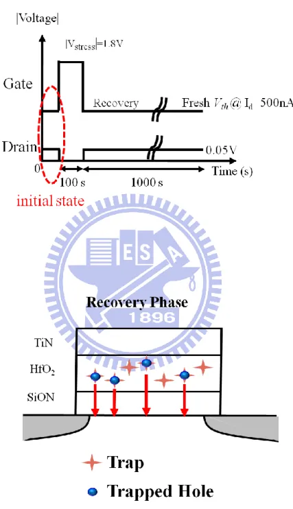
(b) Schematic illustration of holes de-trapping formation during NBTI recovery.
11.
Fig. 2.4 We can extract vth and e from the stair-like threshold voltage trace in NBTI recovery.
12.
Fig. 2.5 Complementary cumulative probability distribution of single de-trapping hole induced vth in NBTI recovery.
13.
Fig. 2.6 When the trapped charge locates on the main current path, it will induce larger vth amplitude.
14.
Fig. 2.7 Individual threshold voltage shift is a stair-like trace. The average threshold voltage shift has logarithmic time dependent in NBTI recovery.
vii
Fig. 2.8 The first three individual de-trapping time (e) probability
distribution are Gaussian-like distribution.
16.
Fig. 2.9 The occurrence of total e distribution is uniform. 17.
Fig. 2.10 Vth versus Number of De-trapping Hole 18
Table I i and i of the first three de-trapping time distribution. 19.
Chapter 3
Fig. 3.1 Schematic representation of band diagram and trap positions in recovery phase.
27.
Fig. 3.2 Flow of Ea extraction 28.
Fig. 3.3 Extracted Ea from e,i Distribution 29.
Fig. 3.4 Flow chart of Monte Carlo simulation. 30.
Fig. 3.5 The probability distribution of trapped charge de-trapping time (e) in NBTI recovery. Monte Carlo simulation result fits the measurement data well.
31.
Fig. 3.6 MC simulation result of total e distribution. 32.
Fig. 3.7 Simulation of stair-like Vth fluctuation. 33.
Fig. 3.8 Probability distribution of NBTI recovery induced Vth at 0.1s, 10s, and 1000s from measurement and Monte Carlo simulation.
34.
Fig. 3.9 The mean value of the Vth distribution versus NBTI recovery time from measurement and Monte Carlo simulation. Percolation has
-function like Ea and ET distribution.
viii
Fig. 3.10 The variance of the Vth distribution versus NBTI recovery time from measurement and Monte Carlo simulation. Percolation has
-function like Ea and ET distribution.
36.
Fig. 3.11 Flow chart of closed form method. 37.
Fig. 3.12 The (a) mean value and (b) variance of the Vth distribution versus NBTI recovery time from Monte Carlo simulation and closed form method.
38.
Table II of extracted Ea from e,1, e,2, and e,3. 39.
Table III and of the first three de-trapping time distribution from measurement and Monte Carlo simulation.
40.
1
Chapter 1
Introduction
For downscaling metal-oxide-semiconductor field-effect-transistor (MOSFET) devices, thickness of gate dielectric is required to be smaller in the progressive technology node. Below the physical thickness of 16 Å , the gate leakage current exceeds the specifications (1 A/cm) [1]. Recently, the high permittivity (high-) dielectrics have been proposed to solve this problem due to its higher physical thickness while keeping the same EOT [2]. Although significant reductions in the gate leakage have been achieved, two major issues remain for CMOS circuit applications: 1) the high threshold voltages [3] and 2) polysilicon (poly-Si) depletion. Consequently, sub-45nm CMOS technology scaling will likely utilize high-/metal gate stacks. And the SiO2 interfacial layer offers better device performance and quality of the oxide/Si interface than high- dielectrics directly placed on the Si substrate.
A high-/metal gate stack is required for scaled MOSFETs, but one of its most serious problems is in Vth control. The BTI degradation of high-/metal gate devices can be seen to be much more severe. NBTI is nowadays the most critical device degradation mechanism and became a limiting factor in scaling of modern CMOS technologies (Fig.1.1) [4]. PMOS Negative Bias Temperature Instability (NBTI) degrades threshold voltage and drive current, raising an important concern for analog and digital circuits. However, NBTI recovery is an important consideration particularly for typical CMOS operation where applied gate bias switches between “high” and “low” voltages repeatedly [5]. Trapped charge would emit when the
2
applied gate bias is “low” voltage which is known as the recovery mode. The NBTI recovery phenomenon leads to a fast reduction of the stress induced electrical device parameter degradation after end of stress. The NBTI recovery phenomenon endangers proper lifetime estimation. In the past, many experimental and theoretical attempts have been made in order to explain the logarithm time dependence of Vth recovery over many decades of time (Fig. 1.2). From these studies, two main NBTI mechanisms have emerged [6]-[9].
In Chapter 2, stair-like drain current traces are observed in the small size devices during NBTI Recovery [10]-[12]. In the recovery phase, the tapped charges emit from the high-k layer by thermal assisted tunneling. Single charge de-trapping induced vth amplitude and its de-trapping time are extracted from the measurement data.
In Chapter 3, it is found that the de-trapping time (e,i) distributions are Gaussian-like distributions. Ea distribution can be extracted from the de-trapping time distributions. We assume that the trap energy distribution is uniform. Based on the distributions of Ea and ET, we simulate the de-trapping time distributions. The de-trapping time distributions are related to the fluctuation of de-trapping hole number. According to the probability distribution of Δvth, each single charge de-trapping induced Δvth amplitude is simulated. Consequently, staircase-like Vth trace during NBTI recovery can be demonstrated a by Monte Carlo simulation. The mean and variance of Vth are acquired during NBTI recovery. We also derive the Vth distribution by closed form method. Finally, we give a conclusion in Chapter 4.
3
Fig. 1.1 NBTI/PBTI induced Vth drift versus stress time in high-/metal gate MOSFETs [4].
4
Fig. 1.2 Recovery data after three selected stress times obtained at different stress voltages [16].
5
Chapter 2
Single Charge Effect in NBTI Recovery
2.1 Preface
It is commonly accepted that mechanism of BTI is due to charge trapping in the high- layer [13]. BTI is characterized by stressing transistor at high temperature and electric field, periodically interrupting the stress to monitor threshold voltage or drain current (“SMS” technique). The other way to investigate BTI effect is to measure post-stress recovery behavior [14].
To identify the charge de-trapping mechanism, a direct measurement of single charge effect is demonstrated, in which the stair-like threshold voltage trace is measured. The Δvth probability distribution is found by extracting the threshold voltage amplitude caused by single charge emission. We also extract single charge de-trapping time, and it is found that the first three individual de-trapping time distribution are Gaussian-like distributions. The occurrence of total de-trapping time distribution is a uniform distribution. According to the tunneling front model, this implies the trap is a uniform distribution in high- layer spatially.
2.2 Device Details and Measurement setup
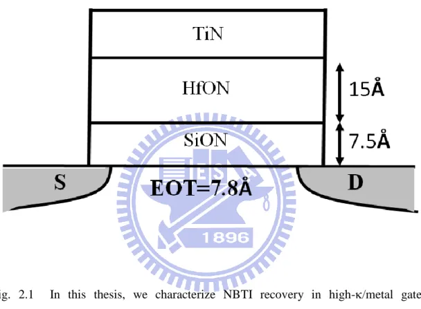
The device structure we used in this thesis is illustrated in Fig. 2.1. The devices are pMOSFETs with a metal gate (TiN) and a bi-layer gate dielectric stack consisting of HfON and interfacial SiON layer (IL). The gate length and width are 30nm and 80nm respectively. Its equivalent oxide thickness (EOT) is 7.8 Å .
6
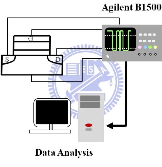
The Measurement setup is shown in Fig. 2.2. A two channel Agilent B1500 pulse generator connects to drain and gate electrode and it changes the gate bias and drain bias simultaneously. The pulse waveform is shown in Fig. 2.3(a). First, we measure the devices initial state to extract fresh Vth @Id=500nA. Then, the devices are subjected to a negative gate bias (Vg=-1.8V) stress during 100s, and recover at fresh
Vth during 1000s. In the recovery phase, the trapping holes will emit by thermally assisted tunneling (TAT), as shown in Fig. 2.3(b).
2.3 Δv
thProbability Distribution in NBTI Recovery
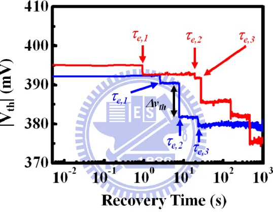
The recovery Vth exhibits a stair-like trace, as shown in Fig. 2.4. Each jump in Fig. 2.4 is believed due to a single trapped hole emission from the high- layer. The
vth amplitude is extracted, as shown in Fig. 2.4. The probability distribution of vth amplitude exhibits an exponential function.
Eq. (2.1)
The cumulative probability distribution, as illustrated in Fig. 2.5, can be expressed below,
Eq. (2.2)
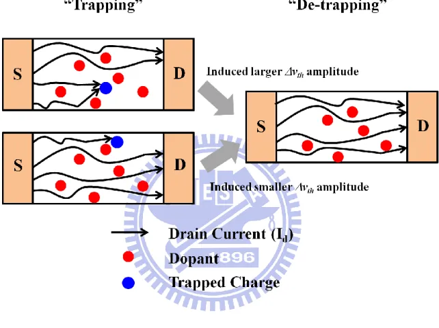
The vth distribution is attributed to a current path percolation effect due to random dopants in substrate (Fig. 2.6) [15]. According to the Eq. (2.2), the slope of the distribution is -1/σ, as shown in Fig. 2.5. The physical meaning of σ is the average
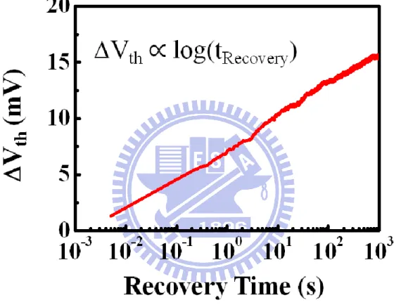
vth induced by single charge de-trapping. Average of each stair-like Vth trace is
1 v exp th th v f
exp th th v f v
7
shown in Fig. 2.7. The Vth versus recovery time follows logarithmic dependence [8],
[16]. This phenomenon is observed in bigger-size devices.
2.4 Single Charge De-trapping Time Distribution
We measure the emission times of the first de-trapping hole (e1), the second
de-trapping hole (e2) and the third de-trapping hole (e3), respectively (Fig. 2.4). The
first three individual de-trapping time distributions (e1, e2and e3
)
are shown in Fig.2.8. It is found that each de-trapping time distribution is a Gaussian-like distribution and their i and i are shown in Table I.
Eq. (2.3)
The de-trapping time (e, i distribution broadens with an increasing the index i.
The occurrence of total e distribution, as shown in Fig. 2.9, is a uniform distribution.
According to the tunneling front model, the traps in the high- are uniform distribution in gate-to-substrate direction.
Eq. (2.4)
2.5
V
thversus Number of De-trapping Hole in NBTI
Recovery
Vth distribution is measured at different recovery times. The total Vth and number of de-trapping hole is extracted. The measurement results at the recovery time
exp(
)
ex
2 , , 2(log(
)
)
1
(log(
))
exp[
]
2
2
e i i e i i if
8
of 0.1(s), 10(s), and 1000(s) are shown in Fig. 2.10. Each data point represents a device. The slope of straight line is the average of single hole de-trapping induced
Vth. As shown in Fig. 2.10., distributions of the de-trapping hole number and Vth broaden with an increasing recovery time.
9
Fig. 2.1 In this thesis, we characterize NBTI recovery in high-/metal gate pMOSFETs with gate length of 30nm and gate width of 80nm.
10
11
(a)
(b)
Fig. 2.3 (a) Waveforms applied to gate and drain during stress and measurement. (b) Schematic illustration of hole de-trapping formation during NBTI recovery.
12
Fig. 2.4 We can extract vth and e from the stair-like threshold voltage trace in NBTI recovery.
13
Fig. 2.5 Complementary cumulative probability distribution of single de-trapping hole induced vth in NBTI recovery.
14
Fig. 2.6 When the trapped charge locates on the main current path, it will induce larger vth amplitude.
15
Fig. 2.7 Individual threshold voltage shift is a stair-like trace. The average threshold voltage shift has logarithmic time dependent in NBTI recovery.
16
Fig. 2.8 The first three individual de-trapping (e) probability distribution are Gaussian-like distribution.
17
18
19
Broader
20
Chapter 3
Simulation of
V
th
Dispersion during NBTI
Recovery
3.1 Preface
Physical origins of Vth distribution during NBTI recovery in pMOSFETs are explored and characterized. Two factors are found to affect a NBTI Vth distribution. One is the dispersion of single charge de-trapping induced vth. The other one is the dispersion of de-trapping time. In the previous chapter, it is found that the first three individual de-trapping time distributions are Gaussian-like distributions. We attribute de-trapping time distribution to activation energy (Ea) and trap energy (ET) distribution in the trapped charge emission model [10]. A statistical model combining the trapped charge emission model with the two dispersions is developed. Our simulation result fits the measured Vth dispersion during NBTI recovery very well. Furthermore, we derive the Vth dispersion using closed form method, and its result fit the measured data very well.
3.2 Extraction E
afrom
e,iDistributions
Single charge phenomenon is measured in the previous chapter. The individual de-trapping time distribution is a Gaussian-like distribution. From the measured e,i distributions, Ea is extracted using trapped charge emission model. The formula of trapped charge emission model is expressed below,
Eq. (3.1) e i, 0
exp(
E
a) exp(
IL ILT
) exp(
kx
i)
kT
21 where
Eq. (3.1-a)
; Eq. (3.1-b)
mIL*=0.41m0 [17] ;mk* =0.18m0 [18]
Eq. (3.1) reveals the nature of tunneling for trapped hole emission time, e, i. Nv is the effective density-of-state in the Si valence band, and Nv(1-fv) is the amount of available states in Si substrate for out-tunneling holes from high-k traps. 0 represents the trap cross-section. Other variables have their usual definitions [10].Energy band diagram is shown in Fig. 3.1. Our estimation is that the trap energy range is about 0.8eV by a 1-D Poisson simulation. ET ranges between 0 and 0.8 eV from the Si valence band. In the formula definition, ET ranges between 2.7 and 3.5 eV in our devices.
The flow of Ea extraction is shown in Fig. 3.2. First, we generate e,i from the measurement data randomly, and we also generate xi randomly. ET is generated by a uniform distribution. As a result, Ea distributions can be calculated, as shown in Fig. 3.3. These Ea distributions are almost the same, and itsstandard deviation of Ea(Ea)) is shown in Table II. The extracted Ea distributions are Gaussian-like distributions.
1 0
[
N
v(1
f
v)
V
th]
* 2 2 IL ( T B) IL m q E * 2 2 k T k m qE 22
3.3 Monte Carlo Simulation of
V
thDistribution
A Monte Carlo simulation employing the trapped charge emission model and taking account the Ea and ET distributions is developed to simulate a Vth distribution and its recovery time evolution. Simulation flow is shown in Fig. 3.4. First, we assume ET is a uniform distribution, and Ea is extracted from e,i distributions. A statistical model combining the trapped charge emission model with the Ea and ET distribution is developed. For reproducing the de-trapping time distribution, we would calculate its average (peak) value first. As illustrated in Fig. 2.8, the trap is a uniform distribution in gate-to-substrate direction. i of each de-trapping time distribution is shown in Table I. It is found that equal about 1. The mean value of ET ((ET) ) equals to 3.1eV. As expressed in Eq. (3.2), we can get the (xi+1-xi). Its value is about 3Å .
Eq. ( 3.2)
MC simulation result is illustrated in Fig. 3.5. Its value is shown in Table III. Simulation result of total e distribution is shown in Fig. 3.6. They all fit the experimental data well.
In our Monte Carlo simulation, an Ea is randomly selected according to extracted
Ea and ET according to a uniform distribution. The single hole de-trapping induced vth dispersion and its de-trapping time distribution are characterized. Consequently, we can demonstrate the stair-like Vth trace during NBTI recovery by MC simulation, as shown in Fig. 3.7. The slope of the dash line corresponds to an average Vth caused
* 1 1 2 2 1 log( ) ( ) ln(10) k i i T i i m q E x x
23
by a trapped hole emission. Fig. 3.8 shows probability distribution of NBTI recovery induced Vth at 0.1s, 10s, and 1000s from measurement and Monte Carlo simulation. The Vth distribution broadens with an increasing recovery time. The simulation results fit the measurement date well, especially in distribution tail. We extract the mean value and the variance of the Vth distribution at different recovery times. The mean value of the Vth follows a logarithm dependence on recovery time in five decades (Fig. 3.9). The variance of the Vth distribution also increases with recovery time (Fig. 3.10). We can’t simulate the Vth distribution and its recovery time evolution exactly when we use the fixed Ea and ET (Percolation Effect). Taking account the Ea and ET distributions is essential to character the Vth distribution during NBTI recovery.
3.4 Closed Form Derivation
In this section, we use another method to derive the Vth distribution during NBTI recovery. Flow chart is shown in Fig. 3.11. Ea is a Gaussian distribution with =0.2(eV) and =0.08(eV). The probability of Ea is expressed below,
Eq. (3.4)
ET is a uniform distribution, and it ranges between 2.7 and 3.5 (eV).
Eq. (3.5)
Taking the probability of Ea and ET into Eq. (3.6), we can get the probability distribution of individual de-trapping time (e,m).
2 2 ( ) 1 ( ) exp[ ] 2 2 a a E f E
(
T)
.
f E
const
24
Eq. (3.6)
With the SRH model, as expressed in Eq. (3.7), we derive the probability distribution of individual de-trapping time (m*).
Eq. (3.7)
Then, we would calculate the de-trapping probability of each m* at different recovery time. P(Am) stands for de-trapping probability of m-th de-trapping hole at a certain recovery time(t).
Eq. (3.8)
P(Bm) stands for the absence of the m-th de-trapping hole, can be expressed below,
Eq. (3.9)
The probability of total amount of m de-trapping holes at a recovery time (t) can be expressed below, Eq. (3.10) , , , * 1 ( ) exp( m ) e m e m e m f ( ) ( *) * t m m P A f
d
(
m)
1
(
m)
P B
P A
0 1 2 3 n 1(
.
0)
P(B ) P(B ) P(B ) ... P(B ) = (
)
M m mP Num
P
P
B
,
(
,
,
)
0exp(
) exp(
) exp(
)
a e m a T m IL IL k m
E
E E x
T
x
kT
25 Eq. (3.11) Eq. (3.12) Eq. (3.13) And so on.
M is the maximum de-trapping number of our measured devices.
As aforementioned, the trap number distribution is calculated and its average and variance are shown in Table IV. A and A are 3.28 (mV). A is the value we measure in Fig. 2.5. Consequently, we can derive the mean and variance of Vth at different recovery time, as expressed below,
Eq. (3.14) Eq. (3.15) Eq. (3.16) And so on. 1 1 1 ( . 1) ( 1) * ( 2) * ( 3) * ( 1) * ( 2) * ( 3) * + ( ) = ( ) ( ) M m M m i i i P Num P P A P B P B P B P A P B P B P A P B
1 2 , 1 ( ) ( ) ( . 2) ( ) ( ) ( ) ( ) M m M m i j i j i j j i P B P Num P P A P A P B P B
1 3 , , 1 ( ) ( ) ( . 3) ( ) ( ) ( ) ( ) ( ) ( ) M m M m i j k i j k i j k k j i P B P Num P P A P A P A P B P B P B
2 2 1 2 n i i x n
0 1 0 2 1 2 2 1 1 1 n n i i n x n
0 1 2 0 1 2 1 2 2 2 2 2 n n n i i n n x n
0 1 0 2 2 2 1 1 1 1 ( ) n n i i n x n
0 1 2 0 1 2 2 2 2 2 2 1 ( ) n n n i i n n x n
26
Eq. (3.17)
Eq. (3.18)
where
;
M is the maximum de-trapping number of our measured devices.
The closed form and Monte Carlo simulation result is shown in Fig. 3.12. The mean and variance of Vth fit the results of Monte Carlo simulation very well.
0 1 2 3 N n n n n i , i=0,1,2,3... i n P N 0 1 0 1 2 0 0 1 2 2 2 2 1 2 2 2 2 2 2 2 2 2 1 1 1 2 2 2 3 3 3 1 1 2 2 M M 2 2 2 1 1 .... n ( + )+n ( + )+n ( + )+... = ( ... ) = ( + ) ( ) n n n n n N i i i i n i n n i
total total total
M M i i i i i i i x x x N N P P P N P P
1 1 2 2 M 1...
=
M total M i i iP
P
P
P
27
Fig. 3.1 Schematic representation of band diagram and trap positions in recovery phase.
28
29
30
31
Fig. 3.5 The probability distribution of trapped charge de-trapping time (e) in NBTI recovery. Monte Carlo simulation result fits the measurement data well.
32
33
34
Fig. 3.8 Probability distribution of NBTI recovery induced Vth at 0.1s, 10s, and 1000s from measurement and Monte Carlo simulation.
35
Fig. 3.9 The mean value of the Vth distribution versus NBTI recovery time from measurement and Monte Carlo simulation. Percolation has -function like
36
Fig. 3.10 The variance of the Vth distribution versus NBTI recovery time from measurement and Monte Carlo simulation. Percolation has -function like Ea and ET distribution.
37
38
(a)
(b)
Fig. 3.12 The (a) mean value and (b) variance of the Vth distribution versus NBTI recovery time from Monte Carlo simulation and closed form method.
39
40
Table III and of the first three de-trapping time distribution from measurement and Monte Carlo simulation.
41
42
Chapter 4
Conclusion
Single charge emission from traps in the high- gate dielectric is observed in small-size devices. Physics of single charge de-trapping induced Vth in NBTI recovery is characterizing in this work. Two factors are found to affect a NBTI Vth distribution. One is the dispersion of single charge de-trapping induced vth. The other one is the dispersion of de-trapping time. The cumulative probability distribution of
vth amplitude follows the exponential distribution. The individual de-trapping time has Gaussian-like distribution. The occurrence distribution of total de-trapping time is a uniform distribution, which implies the trap is a uniform distribution in high- layer spatially.
From the measured e,i distributions, Ea is extracted using trapped charge emission model. The extracted Ea is a Gaussian-like distribution. According to the vth amplitude distribution and the de-trapping time obtained from the experiment, a Monte Carlo simulation employing the trapped charge emission model and taking account the Ea and ET distributions is developed to simulate a Vth distribution and its recovery time evolution. We extract the mean value and the variance of the Vth distribution at different recovery times. The mean value of the Vth follows a logarithm dependence on recovery time. The Vth distribution broadens with an increasing recovery time. Furthermore, we also calculate the mean value and the variance of the Vth distribution at different recovery times using closed form method. These two simulation results fit the experimental data well.
43
Reference
[1] J. Robertson, “Interfaces and defects of high-K oxides on silicon,” Solid
State Electron, vol. 49, no. 3, pp. 283-293, 2005.
[2] G. D. Wilk, R.M. Wallace, and J. M. Anthony, “High-k gate dielectrics: Current status and materials properties considerations,” J. Appl. Phys., vol. 89, no. 10, pp.5243-5801, 2001.
[3] C.Fobbs, L. Fonseca, V. Dhandapani, S. Samavedam, B. Taylor, J. Grant, L.Dip, D. Triyoso, R. Hegde, D. Gilmer, R.Garcia, D.Roan, L.Lovejoy, R. Rai, L. Hebert, H. Tseng, B. White, and P. Tobin, “Fermi level pinning at the poly-Si/metal oxide interface,” in VLSI Symp. Tech. Dig., pp. 9-10, 2003. [4] S. Zafar, Y.H. Kim, V. Narayanan, C. Cabral Jr., V. Paruchri, B. Doris, J.
Stathis, A. Callegari, and M. Chudzik, “A Comparative Study of NBTI and PBTI (Charge Trapping) in SiO2/HfO2 Stacks with FUSI, TiN, Re Gates,” in VLSI Symp. Tech. Dig., pp. 23-25, 2006.
[5] V. Reddy, A.T. Krishnan, A. Marshall, J.Rodriguez, S. Natarajan, T. Rost, S. Krishnan, “Impact of negative bias temperature instability on digital circuit reliability,” in Microelectronics Reliability., Vol. 45, pp. 31–38, 2005 [6] M.A. Alam, and S. Mahapatra, “A comprehensive model of PMOS NBTI
degradation” in Microelectronics Reliability., pp. 71-81, 2005.
[7] H. Kufluoglu, and M.A. Alam, “A generalized reaction-diffusion model with explicit H–H2 dynamics for negative-bias temperature-instability (NBTI) degradation,” IEEE Trans. Electron Devices, vol. 54, no. 5, pp. 1101-1107, 2007.
44
[8] T. Grasser, B. Kaczer, W. Goes, H. Reisinger, T. Aichinger, P. Hehenberger, P.-J. Wagner, F. Schanovsky, J. Franco, M. Toledano, and M. Nelhiebel, “The Paradigm Shift in Understanding the Bias Temperature Instability:From Reaction-Diffusion to Switching Oxide Traps,” IEEE Trans. Electron
Devices, vol. 58, no. 11, pp. 3652-3665, 2011.
[9] V. Huard, M. Denais, and C. Parthasarathy, “NBTI degradation: from physical mechanism to modeling,” in Microelectronics Reliability., Vol. 46, pp. 1–23, 2006
[10] T. Wang, C.T. Chan, C.J. Tang, C.W. Tsai, H.C.-H. Wang, M.H. Chi, and D.D. Tang, “A Novel Transient Characterization Technique to Investigate Trap Properties in HfSiON Gate Dielectric MOSFETs─From Single Electron Emission to PBTI Recovery Transient,” IEEE Trans. Electron Devices, vol. 53, no. 5, pp. 1073-1079, 2006.
[11] C.T. Chan, H.C. Ma, C.J. Tang, and T. Wang, “Investigation of Post-NBTI Stress Recovery in pMOSFETs by Direct Measurement of Single Oxide Charge De-Trapping,” in VLSI Symp. Tech. Dig., pp. 90-91, 2005.
[12] C.T. Chan, C.J. Tang, C.H. Kuo, H.C. Ma, C.W. Tsai, H.C.-H. Wang, M.H. Chi, and T. Wang, “Single-Electron Emission of Traps in HfSiON as High-k Gate Dielectric for MOSFETs,” in Proc. IRPS, pp.41-44, 2005.
[13] A. Shanware, M.R. Visokay, J.J. Chambers, A.L.P. Rotondaro, H. Bu, M.J. Bevan, R. Khamankar, S. Aur, P.E. Nicollian, J. McPerson, and L, Colombo, “Evaluation of the Positive Biased Temperature Stress Stability in HfSiON Gate Dielectrics,” in Proc. IRPS, pp.208-213, 2003.
45
[14] S. Rangan, N. Mielke, and E. C.C. Yeh, “Universal Recovery Behavior of Negative Bias Temperature Instability,” in IEDM Tech. Dig., pp. 341-344, 2003.
[15] A. Asenov, R. Balasubramaniam, A.R. Brown, and J.H. Davies, “RTS Amplitudes in Decananometer MOSFETs:3-D Simulation Study,” IEEE
Trans. Electron Devices, vol. 50, no. 3, pp. 839-845, 2003.
[16] T. Grasser, B. Kaczer, W. Goes, Th. Aichinger, Ph. Hehenberger, and M. Nelhiebel, “A Two-Stage Model for Negative Bias Temperature Instability,” in Proc. IRPS, pp.33-44, 2009.
[17] H.Y. Yu, Y.T. Hou, M.F. Li, and D.-L. Kwong, “Hole Tunneling Current Through Oxynitride/Oxide Stack and the Stack Optimization for p-MOSFETs,” IEEE Electron Device Lett., vol. 23, no. 5, pp. 285-287, 2002. [18] Y.T. Hou, M.F. Li, H.Y. Yu, Y. Jin, and D.-L. Kwong, “Quantum Tunneling
and Scalability of HfO2 and HfAlO Gate Stacks,” in IEDM Tech. Dig., pp. 731-734, 2002.
46
![Fig. 1.1 NBTI/PBTI induced V th drift versus stress time in high-/metal gate MOSFETs [4]](https://thumb-ap.123doks.com/thumbv2/9libinfo/8384326.178355/13.892.201.668.298.780/nbti-pbti-induced-drift-versus-stress-metal-mosfets.webp)
![Fig. 1.2 Recovery data after three selected stress times obtained at different stress voltages [16]](https://thumb-ap.123doks.com/thumbv2/9libinfo/8384326.178355/14.892.180.711.307.790/recovery-selected-stress-times-obtained-different-stress-voltages.webp)