國立交通大學
電子工程學系 電子研究所碩士班
碩士論文
雙閘極奈米線非揮發性記憶元件之研製與分析
Fabrication and Characterization of Double-Gated
Nanowire SONOS Devices
研 究 生 : 江忠祐
指導教授 : 林鴻志 博士
黃調元 博士
雙閘極奈米線非揮發性記憶元件之研製與分析
Fabrication and Characterization of Double-Gated
Nanowire SONOS Devices
研 究 生 : 江忠祐 Student: Chung-Yu Chiang 指導教授 : 林鴻志 博士 Advisors: Dr. Horng-Chih Lin 黃調元 博士 Dr. Tiao-Yuan Huang
國立交通大學
電子工程學系 電子研究所碩士班
碩士論文
A Thesis
Submitted to Department of Electronics Engineering & Institute of Electronics College of Electrical and Computer Engineering
National Chiao-Tung University in Partial Fulfillment of the Requirements
for the Degree of Master in
Electronic Engineering July 2008
Hsinchu, Taiwan, Republic of China
雙閘極奈米線非揮發性記憶元件之研製與分析
研究生:江忠祐 指導教授:林鴻志 博士 黃調元 博士國立交通大學
電子工程學系 電子研究所碩士班
摘 要
在本篇論文中,我們成功地利用邊襯蝕刻技術(sidewall spacer over-etching technique)製作出具有奈米線通道的薄膜記憶體結構。同時,我們也利用雙閘極 結構,對於元件的基本電性以及寫入/抹除特性做詳盡的研究與分析。
由於奈米線與雙閘極結構具有高表面體積比(high surface-to-volume ratio)能 有效提升閘極控制能力,且在降低短通道效應與次臨界擺幅(subthreshold swing) 方面都有顯著的改善。在此奈米線結構中,氮化矽覆蓋層被證實能有效降低漏電 流。另外,利用雙閘極結構,我們提出一種新的「可調變式寫入/抹除速度」的 方法。在一最佳化偏壓條件下,不需改變元件材料或介電層厚度就能有效提升寫 入/抹除速度。然而,可靠度的表現需要有效地被改善,例如在通道形狀、製程 步驟或是介電層材料方面著手,才能在實際上有所應用。
Fabrication and Characterization of Double-Gated
Nanowire SONOS Devices
Student: Chung-Yu Chiang Advisors: Dr. Horng-Chih Lin Dr. Tiao-Yuan Huang
Department of Electronics Engineering and Institute of Electronics National Chiao Tung University, Hsinchu, Taiwan
ABSTRACT
In this thesis, nanowire SONOS devices were fabricated by use of sidewall spacer over-etching technique. Furthermore, the fabricated devices were equipped with double-gated configuration. Impacts of the structural features on basic transfer characteristics and programming/erasing (P/E) characteristics were investigated and discussed in detail. It was found that the nanowire channel and double-gated structures were capable of enhancing the gate controllability by taking advantage of high surface-to-volume ratio, and led to improved characteristics such as reduced short channel effects and better subthreshold swing. To reduce the off-state leakage, the adoption of a silicon nitride (SiN) hardmask layer was demonstrated. Besides, a new concept of modulating the P/E speed with the double-gated operation was also proposed in this thesis. It was shown that the P/E speed could be enhanced with an optimized biasing condition. Nevertheless, the reliability characteristics of the NW SONOS devices remain an issue for practical application. Further optimizations in NW shape, process condition, as well as the ONO structure are needed.
A
A
c
c
k
k
n
n
o
o
w
w
l
l
e
e
d
d
g
g
e
e
m
m
e
e
n
n
t
t
在論文尚未著手的時候,我的誌謝已經完成。 很開心也很慶幸可以加入交大屬一屬二的研究團隊,帶領這個團隊的大家長 黃調元教授與林鴻志教授給學生很多自由空間、想像力量。不只言教,在做人處 事的學習上也有很大的啟發。短短三兩行無法描述對兩位老師的感激,僅此向老 師們表達謝意。 研究所這一階段,著實獲益良多,對於半導體工程的了解有更深一層的著 墨,這是由衷的感覺。在七百多個日升月落中,大半的心力都投注在課業的研究 上面:碩一跟著實驗室 meeting 感覺鴨子聽雷,還好腦袋尚可以應付研究所課程 而不至灰心喪志;碩二日夜顛倒趕著完成元件,還好出來的成果尚可撫慰我疲憊 的心靈而不至自怨自艾。基本上,我是幸運的、開心的、有收穫的。 這兩年的生活,首先要感謝大偉劉同學兼室友,從我踏上新竹的第一步就開 始接受他的照顧,直到離開新竹的最後幾天也是住在他的新家。在日復一日的研 究生活中,我們添加了一些逛街、投籃機、以及水族生活。另外,更要感謝引領 我做實驗的阿森、徐博、Benson、TZI 以及哲民等學長。從徐博身上我聞到了成 熟男人的味道;從 Benson 身上我看到了純潔大男孩的影子;從 TZI 身上我感覺 到交大(宅)版吳宗憲的存在。在同梯裡,大師感謝你在研究上不吝與我討論,是 我們良好的學習楷模;大雄感謝你除了課業上的討教,打球都讓我電使我生活多 了點小樂趣;樟樟感謝你那個那個以及生活上很多的幫忙,只差沒有給你好人 卡;HCLin 感謝你熱心幫忙,很多事情都仰賴你的幫助;小強感謝你給我很多思 考上的學習;最後是女生:陳玲感謝你總為實驗室劃破了那寂靜,帶給許多人歡 樂。其它新進的學弟學妹,除了好好學習之外,也不要忘了散發知自己的青春活 力(以上順序依照筆劃排序)。 除了實驗室成員外,也很開心認識了弘森,彼此在實驗上互相打氣,也在生 活上互相加油。另外我的室友施議森與傅英哲,因為你們,讓我度過很愉快的研 究所生活,同時也感謝你們容忍我半夜打呼、早上打噴嚏的習慣。 在此要感謝我的女朋友,玨瑤,在我研究不順利的時候幫我打氣加油,並且 給我生活上許多扶持與鼓勵。 最後要感謝最重要的家人。感謝爸爸媽媽提供我衣食無缺的生活條件,也提 供我ㄧ個溫暖的家,讓我可以專心的學習,希望我的表現會讓你們感到驕傲。 2008.7C
C
o
o
n
n
t
t
e
e
n
n
t
t
s
s
Chinese Abstract
………IEnglish Abstract
………IIAcknowledgment
………IIIContents
………IVFigure Captions
………VIChapter 1 Introduction
…………11-1
Overview of SONOS-Type Memory Devices
………11-2
Overview of Double-Gate Technology
………41-3
Motivation and Intention of this Study
………51-4
Thesis Organization
………5Chapter 2 Device Fabrication and Basic Concepts of
SONOS Memory Devices
………
………72-1
Device Fabrication
………72-2
Program and Erase Mechanisms
………82-2-1 Channel Hot Electron Injection………9
2-2-3 Band to Band Tunneling ………10
2-3
Reliability Issues
………11Chapter 3 Results and Discussion
………133-1
Basic Transfer Characteristics
………133-1-1 General Backgrounds ………13
3-1-2 Leakage Current ………14
3-1-3 Threshold Voltage Modulation ………18
3-2
Program/Erase Characteristics
………193-2-1 Basic Program/Erase Operation………19
3-2-2 Application of Double-Gate Structure in SONOS………21
3-2-3 Improve Program/Erase Speed with Optimized Top-Gate Voltage ………22
Chapter 4
Conclusion and Futrue Work
………244-1 Conclusion
………244-2 Future Work
………25References
………27Figures
………34F
F
i
i
g
g
u
u
r
r
e
e
C
C
a
a
p
p
t
t
i
i
o
o
n
n
s
s
Chapter 1
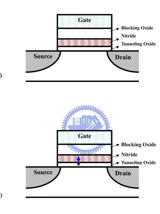
Fig. 1-1 (a) A floating-gate memory structure. The floating-gate is made of polysilicon and is surrounded by insulator. (b) A single defect in insulator will cause the loss of all stored charges ………34 Fig. 1-2 (a) A SONOS-type memory structure. The dielectric is replaced with an
oxide-nitride-oxide (ONO) layer. (b) Due to discrete-trap nature, single SILC path in the tunnel oxide will not completely drain the stored charges from the nitride………35 Fig. 1-3 Band diagrams of MOS structures with different kinds of gate
dielectrics ………36
Chapter 2
Fig. 2-1 Top views of (a) single-gated and (b) double-gated NW SONOS
structures ………37
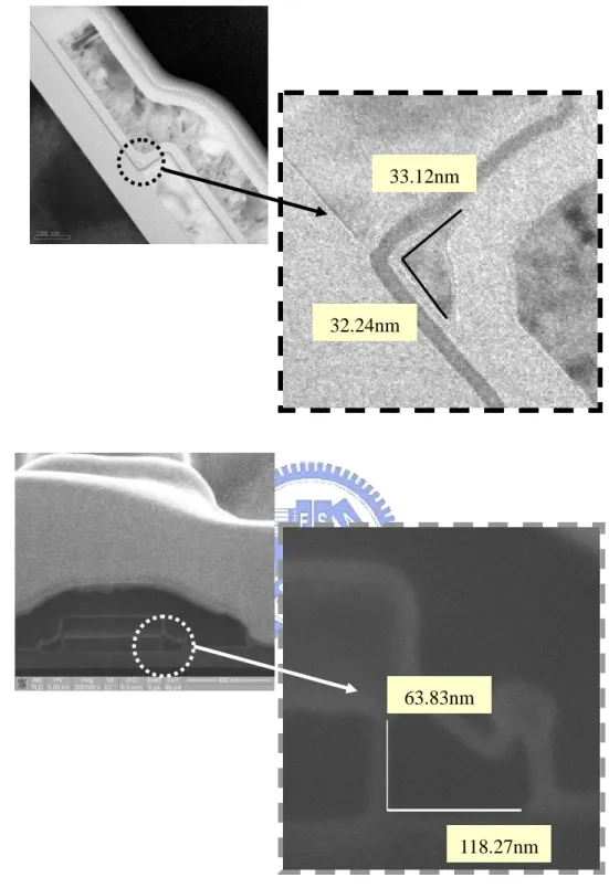
Fig. 2-2 Cross-sectional views of double-gated NW SONOS structures with (a) and without (b) nitride capping ………38 Fig. 2-3 (a) TEM image of NW-SONOS, and (b) SEM image of HM-SONOS …39 Fig. 2-4 Channel hot electron injection is used for programming. Electrons are
accelerated by the high lateral electric field; gain enough energy to overcome the interface barrier, and then are trapped in the storage
occurs when Etox is larger than
tox t qφ1
. (c) Direct tunneling occurs when Etox is
smaller than
tox t qφ1
………41
Fig. 2-6 Band to band tunneling. (a) When biasing a large negative voltage on gate electrode in an n-channel device, a deep depletion region appears in the overlap of gate and drain. (b) Holes will be attracted by the negative gate bias to tunnel into the storage nitride layer ………42 Fig. 2-7 Typical characteristics of threshold voltage evolution with retention time.
The difference between fresh and P/E cycled devices is related to the charge trapped in the oxide and resulting in reliability degradation ………43 Fig. 2-8 Major leakage paths from storage trapping sites. One is thermionic
emission and the subsequent Frenkel-Poole mechanism (solid line). Another is charge-assisted-tunneling mechanism (dashed line) ………44 Fig. 2-9 Endurance failure in SONOS devices ………45
Chapter 3
Fig. 3-1 The configuration of measured setting, which includes an HP-4156A for I-V measurement, an Agilent-E5250A acting as a switch, and an Agilent-8810A acting as a pulse generator ………46
Fig. 3-2 Transfer characteristics of (a) NW-SONOS and (b) HM -SONOS devices operated under SG mode, TG mode, and DG mode. The sum of the SG and TG modes is also shown for comparison………47 Fig. 3-3 Off-state current of NW-SONOS devices as a function of gate width …48
Fig. 3-4 Off-state current of HM-SONOS devices as a function of gate width …49
operation with (b) large gate width and (c) small gate width, and for TG mode with (d) large gate width and (e) small gate width ………50
Fig. 3-6 Measured ID-VG curves of a NW-SONOS device under (a) SG mode of
operations with various top-gate voltages, and (b) TG mode of operations with various side-gate voltages ………51 Fig. 3-7 Measured ID-VG curves of a HM-SONOS device under (a) SG mode of
operations with various top-gate voltages, and (b) TG mode of operations with various side-gate voltages ………52 Fig. 3-8 (a) Programming and (b) erasing characteristics under various stress
voltages. Black lines are measured in NW-SONOS, and gray lines in HM-SONOS.………53 Fig. 3-9 Band diagrams under (a) programming and (b) erasing operations………54 Fig. 3-10 (a) Schematic band diagram of NW-SONOS devices with P-type and
N-type side-gate under erasing operation. Electron tunneling from the gate is effectively blocked with the P-type gate. (b) Comparisons of erasing efficiency of NW-SONOS devices with P-type and N-type side-gate …55 Fig. 3-11 Log-ID vs. side-gate voltage of different states in (a) NW-SONOS and (b)
HM-SONOS devices ………56 Fig. 3-12 Linear-ID vs. side-gate voltage of different states in (a) NW-SONOS and (b)
HM-SONOS devices ………57 Fig. 3-13 Delta Vth versus time in (a) programmingand (b) erasing operation under SG, TG, and DG modes ………58 Fig. 3-14 Shift in Vth as a function of the applied top-gate voltage for NW-SONOS devices after (a) programming and (b) erasing ………59 Fig. 3-15 (a) Programming and (b) erasing characteristics of the NW-SONOS
Fig. 3-16 Shift in Vth as a function of the applied top-gate voltage for HM-SONOS devices after (a) programming and (b) erasing ………61 Fig. 3-17 ID-VG curves of HM-SONOS devices evolving with erasing time under (a)
VTG=0V and (b) VTG=3V ………62
Chapter 4
Fig. 4-1 Illustration of independent side-gate structure. Two-bit operation can be
Chapter 1
Introduction
1-1
Overview of SONOS-Type Memory Devices
In recently year, the market for personal portable electronic products, such as
MP3 players, digital cameras, cell phones, and external storage devices, grows
explosively. Therefore, the industry of nonvolatile memory (NVM) is stimulated
profoundly.
According to International Technology Roadmap for Semiconductors (ITRS) [1],
however, there are several challenging issues lying ahead for NVMs to achieve
low-power and high-reliability performance. This forecast is based on the structure
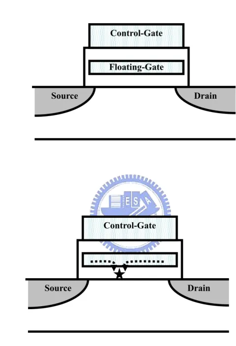
and material of floating-gate (FG) NVM devices, as illustrated in Fig. 1-1(a). Since
the storage layer of floating-gate device is made of conducting polysilicon, just a
cluster of two or three defects in the tunneling oxide will lead to a dramatic increase
in leakage (so-called stress induced leakage current-SILC) and cause severe loss of all
stored charges, as illustrated in Fig. 1-1(b). This issue has actually put a scaling limit
on the thickness of tunnel oxide at around 8 nm, which seriously affects the down
A lot of candidates have been proposed for succeeding the FG flash devices, such
as ferroelectric memories, magnetic memories, and phase-change memories. Among
these candidates SONOS-type memory, as illustrated in Fig. 1-2(a), is the most
promising because of process simplicity and the maturity in preparation of the
materials involved in the structure. Instead of using a floating-gate, the storage layer
of SONOS-type device is nitride. Due to the insulator nature of nitride, charges stored
in the material are discrete, making the storage much less sensitive to the SILC. As
illustrated in Fig. 1-2(b), a leakage path via the defect formed in the tunnel oxide may
only de-trap the charge stored in a discrete-trap. According to the storage property of
nitride, tunneling oxide thickness can be scaled down much more easily and
low-power operation can be realized [2]. Moreover, by discrete-trapping, a new 2-bits
NVM concept, named NROM, is evolved, which uses channel hot electrons (CHEs)
for programming, hot holes for erasure, and using a reverse-read scheme. In this way,
high-density NVMs can be accomplished without scaling down the feature size of the
technology [3].
A number of papers have been published for developing high performance and
high reliable SONOS. One approach is to modify the composition of the sandwiched
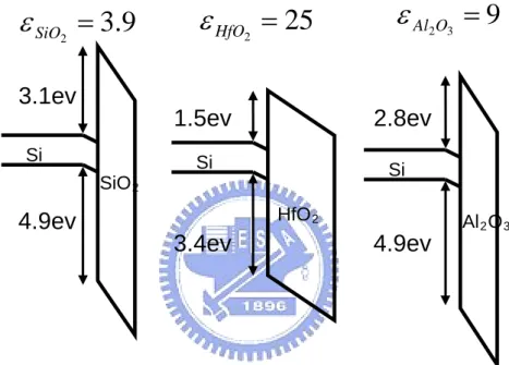
dielectric layer [4]-[12]. For example, Samsung proposed the use of a high-κmaterial,
tends to increase the field strength of tunnel oxide, so the P/E efficiency could be
enhanced. On the other hand, the field strength in the block oxide is reduced, which is
helpful to increase the erase window [4]-[6]. Replacing the nitride with HfAlO or
nano-dots is also proposed [7]-[9]. These materials provide a suitable band diagram
offset to obtain fast programming, and a relatively low operation voltage can be used.
Figure 1-3 shows the band diagrams for MOS devices with gate dielectrics of SiO2,
HfO2, and Al2O3, respectively.
Replacing the tunneling oxide with sandwiched oxide-nitride-oxide also can
suppress direct tunneling at low electric field [10]-[13], which is helpful for retention
performance improvement. It also allows a more efficient hole tunneling process
during erase at a high electric field due to the insertion of the ultra-thin nitride in the
tunnel gate dielectric.
New operation schemes may also improve device reliability. A new erase
technique that combines the benefits of FN tunneling erase and hot-hole injection
erase has been shown to improve P/E speed and reliability issues [14]. A similar
concept of soft erase and re-fill processes is introduced to obtain excellent endurance
and retention [15]. Programming by hot hole injection nitride electron storage
1-2
Overview of Double-Gate Technology
As CMOS technology is scaled down to 45 nm and beyond, the reduction of
subthreshold and gate-dielectric becomes essential. As channel length reduces, the
electric field generated from the drain exhibits a stronger influence on the channel
potential. If not handle carefully, it may even loss the capability of the gate control to
turn off the channel conduction. In a double-gate (DG) metal-oxide-semiconductor
field effect transistor (MOSFET), the electric field from the drain side can be
effectively shielded from penetrating into the channel by the second gate. Therefore,
the DG-MOSFET becomes one of the most popular candidates to overcome the
obstacles imposed by the short-channel effects. Moreover, additional benefits like
mobility enhancement and higher current drive are also demonstrated [17]-[20].
Many studies about DG-MOSFET are devoted to address and to improve
performance. To optimize Vth of DG-MOSFET, asymmetric double-gate has been
proposed by using different gate work-function materials, such as n+/p+ gate [21] [22].
Furthermore, steeper SS and higher Ion can be achieved by asymmetric gate stacks
[23].
The DG MOSFET can be operated by applying independent voltages to the two
appropriately according to the requirement during circuit operation. This provides
extra freedoms for optimization of circuit speed and power consumption.
1-3
Motivation and Intention of this Study
In order to improve the performance of TFT-SONOS devices, nanowire channel
and double-gated configuration are useful approaches to overcome the obstacles. For
example, poor subthreshold swing and leakage current in TFT-SONOS result in weak
programming/erasing efficiency and power consumption. These shortcomings are
expected to be improved by nanowire channel and double-gated configuration due to
better SCE suppression and gate controllability. However, few works that studied the
effect of applying both approaches on the performance of SONOS devices are found
in the literature. This motivates us to carry out this study. Moreover, the mechanism of
programming/erasing efficient improvement by double-gated configuration will be
discussed, and the suppression of leakage current will also be analyzed.
1-4 Thesis
Organization
flow, and basic concepts about the measurements of SONOS-type memory devices
are described. Then, measured data, including basic electrical and program/erase
characteristics, are discussed and analyzed in Chapter 3. Finally, in Chapter 4, we
summarize the important conclusions of this study, and suggestions for future work
Chapter 2
Device Fabrication and Basic
Concepts of SONOS Memory
Devices
2-1 Device
Fabrication
At first, a silicon dioxide of 100nm was thermally grown on 6-inch wafers.
Then, 100nm-thick n+-doped poly-silicon serving as a gate electrode (side-gate), and a
100nm nitride serving as hard-mask layer were sequentially deposited. The
polysilicon and nitride were patterned with a lithography step and then etched to form
a rectangle structure, followed by the deposition of an ONO stacked layer with a total
thickness of 18 nm, consisting of a 7nm-thick blocking oxide grown at 700℃ in a
low-temperature chemical vapor deposition (LPCVD) system with
tetra-ethyl-ortho-silicon (TEOS) as the precursor, an 7nm-thick LPCVD
silicon-nitride layer deposited at 780℃, and a 4nm-thick tunneling oxide LP-TEOS
grown at 700℃. Afterwards, a 100nm-thick amorphous-silicon layer was deposited by
LPCVD. After an annealing step at 600℃ in N2 ambient for 24 hours to transform the
performed with a sufficiently low implant energy to ensure the majority of dopants
was located near the surface. S/D photoresist patterns were then formed on the
substrate by a standard lithography step. In order to form the sidewall polysilicon
nanowire channel in a self-aligned manner, a reactive plasma etching step was used.
Afterwards, S/D regions were heavily doped while the channels remained undoped.
Then a 24nm-thick LP-TEOS oxide and a 100nm-thick n+-doped poly-silicon were
deposited and employed as the top gate oxide and top gate electrode. A 300nm-thick
LP-TEOS oxide serving as the passivation layer was subsequently deposited. Finally,
the fabrication was completed after the formation of contact hole and metallization.
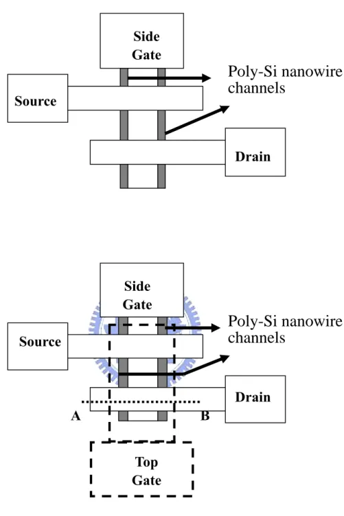
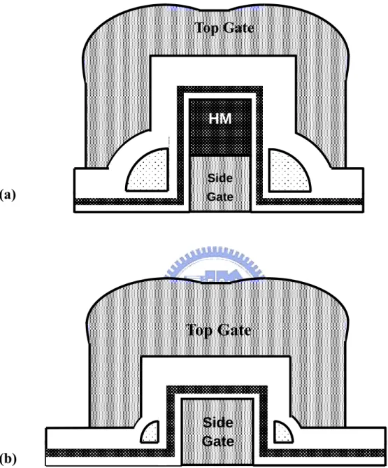
In addition to the aforementioned doubled-gate configuration, single-gate
devices were also fabricated by skipping the top gate oxide and top gate electrode
formation steps. Also noted for the single-gate device is that, unlike the double-gate
ones, no nitride capping was applied on the top of the side-gate electrode. Top views
of single-gate and double-gate nanowire-SONOS structures are shown in Figs. 2-1(a)
and 2-1(b), respectively. Cross-sectional views of side-gate with and without nitride
capping are displayed in Figs. 2-2(a) and 2-2(b), respectively.
The Vth of SONOS-type devices can be modulated by the operations of program
and erase. Carriers are trapped or de-trapped in the storage dielectric layer to change
the state of Vth. Mechanisms such as channel-hot-electron injection (CHEI),
Fowler-Nordheim Tunneling (FNT), and band-to-band tunneling (BTBT) are
employed for the purpose. These mechanisms will be discussed in the following
sections.
2-2-1 Channel Hot Electron Injection
The hot-carrier effect on MOSFET had been widely investigated since the 1970s.
While a transistor is biased under strong inversion with Vds > Vdssat, a pinch-off
point occurs near the drain side in the channel where a strong lateral electric field may
exist. Electrons will be accelerated by the high lateral electric field and gain energy.
According to the ‘lucky-electron model’ [24], some electrons may gain enough energy
to overcome the interface barrier and will be injected into the gate oxide, as illustrated
in Fig. 2-4. In general, the injection from Si to SiO2 is more difficult for holes than for
electrons owing to the heavier effective mass and higher barrier height. Therefore,
2-2-2 Fowler-Nordheim Tunneling
Tunneling mechanism is a quantum mechanical process whereby electrons tunnel
through the forbidden band of oxide under a high electric field. According to the
strength of electric field across the insulator, the tunneling mechanisms can be
classified into two types. The first type occurs when the electric field strength across
tunneling oxide (Etox) is larger than
tox t qφ1
, where φ is the barrier height of conduction 1
band between oxide and silicon substrate, and is denoted as the Fowler-Nordheim
Tunneling [25]. The other type is the direct tunneling which occurs when Etox is
smaller than
tox t qφ1
. Figure 2-5 shows the two type of tunneling mechanisms. Usually, a
large positive (or negative) voltage bias is applied to the gate electrode to induce the
FNT current and injects electrons (holes) through tunnel oxide layer. Some of these
injected carriers are then trapped in the nitride layer. The tunneling current density is
expressed as ) 3 2 4 exp( 16 2 3 2 2 3 ox ox ox ox FN q m q J Φ − Φ = ∗ η η φ φ π ,
where Φox is the field across oxide, η is the Planck’s constant, is the effective
mass, and
*
m
ox
φ is the barrier height.
2-2-3 Band to Band Tunneling
field across the reverse-biased junction is high enough to form a deep-depletion
region, as illustrated in Fig. 2-6(a). Usually, a negative gate voltage is applied for
n-channel devices. In this situation, electrons tunnel directly or are assisted by traps in
the gap from valance band into the conduction band. On the other hand, holes are
generated in the deep-depletion region at the same time and could be attracted by the
negative gate bias to tunnel into the storage nitride layer, as illustrated in Fig. 2-6(b).
2-3 Reliability Issues
Nonvolatile flash memory has become an indispensable component in modern
portable storage products. With aggressive scaling-down, internal leakage current
becomes a major issue on reliability and a crucial concern in determining the life-time
of digital products.
Data retention refers to the ability to retain a data state over a period of time no
matter the power is on or off. After program/erase (P/E) cycles, the threshold voltage
of the programmed state typically decreases with retention time while the threshold
voltage of the erased state typically shifts positively, resulting in the shrinkage of the
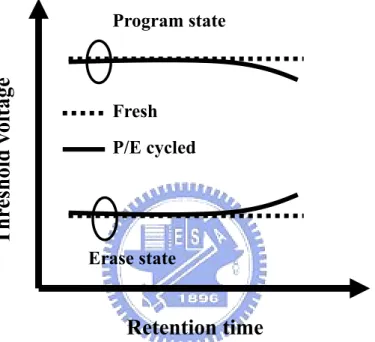
memory window [26]. This is illustrated schematically in Fig. 2-7. Data retention loss
shows major leakage paths from storage trapping sites [27]. For SONOS devices,
threshold voltage of the programmed state drops due to laterals electron migration and
oxide-trap-assisted tunneling through bottom oxide; positive charges in tunneling
oxide are created during P/E cycles and assist electrons to tunnel from active region to
nitride layer, causing the drift of threshold voltage in the erased state.
Charge trapping in oxide brings another major reliability concern, namely, the
endurance [28]. Endurance is defined by the number of P/E cycles without departing
from the specifications. Unlike floating-gate memories which typically exhibit
window closure problems, SONOS memories reveal a different trend: the threshold
voltages of programmed and erased states both move upward, as shown in Fig. 2-9. It
is believed that charge trapping in the tunnel oxide is responsible for the endurance
Chapter 3
Results and Discussion
3-1
Basic Transfer Characteristics
3-1-1 General Backgrounds
In this study the electrical characteristics of the fabricated devices are all
characterized by a measurement system regulated by a personal computer. The system
contains an HP-4156A parameter analyzer for I-V measurement, an Agilent-E5250A
switch, and an Agilent-8810A pulse generator. Configuration of the system is shown
in Fig. 3-1.
Usually two methods are used to determine the threshold voltage (Vth). One is to
simply define the Vth as the VG corresponding to a specific drain current. The other is
the extrapolated VG from the linear-ID versus VG curve. Usually the point on the
ID-VG curve corresponding to the occurrence of Gmmax is used to for the
extrapolation. However, due to a large amount of defects contained in the grain
boundaries of the poly-Si channel in TFTs, often it is not easy to find a distinct
maximum peak in the Gm-VG plot of the devices. Therefore, we decide to use the
In this study, FN tunneling is employed for programming and erasing rather than
CHEI/CHHI. It is generally difficult for carriers transporting from source to drain to
gain sufficiently high energy to overcome the barrier height of Si/SiO2 owing to
plenty of scattering centers presenting in the poly-Si channel. Therefore, the
efficiency of hot electron injection is dramatically suppressed. Since the fabricated
devices have four terminals and each of them is applied with a specific voltage during
the operation, in the thesis the denotation for the bias conditions is expressed as (A, B,
C, D), in which A, B, C, and D are the voltages applied to side-gate, top-gate, drain,
and source, respectively. For example, (15, 4, 0, 0) denotes that the side-gate is
applied with 15 voltage, the top-gate is applied with 4 voltage, and both drain and
source are grounded.
3-1-2 Leakage Current
Figures 3-2(a) and 3-2(b) show the transfer characteristics of NW-SONOS and
HM-SONOS devices in SG-mode, TG-mode, and DG-mode, respectively. SG-mode
denotes that the voltage applied to the side-gate is being swept, while a constant
voltage is applied to the top-gate. In the following discussion the constant voltage
stated above is set to zero if not specified. TG-mode is contrary to the bias
while a constant voltage is applied to the side-gate. DG mode means the two gates are
tied together and applied with the sweeping voltage. Also shown in the figures is the
sum of the SG and TG modes for comparison purpose.
An obvious noticeable difference between Fig. 3-2(a) and 3-2(b) is the
off-current in SG-mode. One of the advantages pertaining to the HM-SONOS device
is to suppress gate-induced drain leakage (GIDL) induced in SG-mode [29]. GIDL
originates from reverse-biased junction in the overlap region between drain and gate,
which strongly depends on field strength wherein. In HM-SONOS, a hard-mask layer
is inserted between the side gate and drain, therefore the field strength is dramatically
weakened. As a result, the GIDL is suppressed dramatically, as shown in Fig. 3-2(b).
Such effect does not appear in TG-mode because the overlap region between the top
gate and the drain has nothing to do with the hard-mask layer. The results shown in
the figures confirm the expectation.
To more clearly illustrate the situation, the off-state leakage current of the
NW-SONOS and HM-SONOS devices operated under both SG mode and TG mode
measured at VG=-4V and VD=3V is expressed as a function of “gate width” in Fig.
3-3 and Fig. 3-4, respectively. The “gate width” refers to the planar width of the
side-gate pattern, as indicated in Fig. 3-5. In Fig. 3-3, we can see that the off-state
conduction occurs in the drain region overlapping the top of the side-gate, as shown in
Figs. 3-5(b) and 3-5(c). The figures in Fig. 3-5 are the cross-sectional views of the
device along the boundary between the drain junction and the NW channel (Line AB
in Fig.3-5(a)). Owing to the large voltage difference between the side-gate and the
drain, the thinner the gate dielectric, as well as the lighter the doping concentration at
the drain/gate dielectric interface, the bigger the GIDL leakage via band-to-band
tunneling with or without the assistance of traps in the junction [29]. For TG mode of
operation, the gate-width dependence in off-state leakage is lifted, as illustrated in Fig.
3-3. This is reasonable, since the flow paths of off-state leakage for TG mode (shown
in Figs. 3-5(d) and 3-5(e)) are actually not through the drain region over the top of
side-gate. Fig. 3-4 indicates that the off-state currents of the HM-SONOS under both
the TG and SG modes of operation are independent of the gate width. In this case, the
same reason as for the NW-SONOS holds for the TG mode, while suppression of the
leakage for the SG mode is due to the use of a hard-mask inserted between the
side-gate and the drain which tends to reduce the field strength and thus the GIDL is
hindered.
In Fig. 3-2, a larger on-current in TG-mode than the SG-mode can be explained
by a larger effective conduction width according to the TEM image, as well as the
schematic flow paths shown Fig. 3-5. As mentioned in Chap.2, a low-energy S/D
implant was performed in device fabrication. As a consequence, a large undoped
offset region actually exists between the n+ doping region and the channel region. In
the case of side-gated conduction, as shown in Figs. 3-3(b) and 3-3(c), the undoped
offset region (surrounded by the dashed line) is actually not gated by the side-gate.
This feature results in a large parasitic resistance and degrades the on-current of the
SG operation. In contrast, the offset region between the n+ doping region and the
top-gated channel region is actually gated by the top gate. Therefore the on-current is
not seriously affected.
Due to the dual-channel conduction in DG-mode, a larger on-current over TG-
and SG-mode can be obtained in Fig. 3-2(a) and 3-2(b). However, it has to be noticed
that the on-current in DG mode is much larger than the sum of SG and TG modes in
Fig. 3-2(a). This is an indication of the occurrence of volume inversion effect [30].
Such effect is due to the coupling of channel potential at different regions of a
multiple-gated device, and becomes profound as the channel body becomes ultra-thin,
such as the case of the NW-SONOS in the present study. The phenomenon is not
observed in Fig. 3-2(b), however, because of the much thicker body in HM-SONOS
3-1-3 Threshold Voltage Modulation
Figures 3-6(a) and 3-6(b) show excellent characteristics about the Vth
controllability of double-gated devices. If the body thickness is sufficiently thin that
complete depletion can occur, coupling of the two channel potential driven by the two
gates becomes significant. As a result, Vth of each gate depends strongly on the bias
conditions of the two gates [31] [32]. When top-gate (or side-gate) is biased on a
constant voltage smaller than VthDG (threshold voltage under DG mode of operation)
the surface potential near top-gate (or side-gate) is depleted. Under this condition,
VthSG (or VthTG) is larger than VthDG. While voltage applied to top-gate (or side-gate)
is larger than VthDG, an inversion layer is present near the top-gate (or side-gate) side,
therefore, smaller VthSG (or VthTG) is obtained. Moreover, top-gate bias has stronger
effect on modulating the Vth than the side-gate, as shown in the figures. This is
ascribed to the larger effective conduction width of the TG conduction.
Figure 3-7 shows the characteristics of the HM-SONOS devices. In this case, the
channel body is much thicker than the former example, so the interaction between two
gates becomes much weaker. As can be seen in Figs. 3-7(a) and 3-7(b), as the voltage
applied to the control gate is sufficiently large to turn on the corresponding gated
channel, the off-state current is large and independent of the sweeping gate voltage.
current presenting on the opposite channel surface due to the thicker channel body.
3-2 Program/Erase Characteristics
3-2-1 Basic Program/Erase operation
Figure 3-8(a) shows the shift of Vth under SG mode of operation versus
programming time under different stressing condition with a high programming
voltage applied to the side-gate. Both NW-SONOS and HM-SONOS are
characterized in the figures. Figures 3-9(a) and 3-9(b) show the band diagram during
programming and erasing, respectively. In Fig. 3-8(a), programming speed is
enhanced as the programming voltage increases. It can also be seen that a larger
memory window can be obtained in NW-SONOS device than the HM-SONOS. This
is suspected to be due to the thinner channel body as well as the horn-like corner. The
two factors can help increase the field strength in the tunnel oxide [33]. Note that,
owing to the special geometry of channel, the horn-like channel lies on the gate
dielectric layer in NW-SONOS devices. However, in HM-SONOS devices, the corner
is shaded by the nitride hard-mask, thus the impact is reduced.
Delta Vth versus erasing time is shown in Fig. 3-8(b). Better erasing efficiency is
the horn-like corner. As erasing voltage increases, erasing speed increases. However,
erase saturation may occur when a large erasing voltage is applied or as the erasing
time is long. This may be attributed to the injection of electrons from gate electrode to
the nitride layer in the erase duration which tends to balance the negative shift of
threshold voltage due to the release of trapped electrons to the channel or injection of
holes from the channel to the nitride storage layer.
Substituting the N-type side-gate with P-type one is a useful method to avoid the
above issue. Figure 3-10(a) illustrates the band diagram of NW-SONOS devices with
P-type and N-type gate during erasing.Owing to the increase in tunneling barrier, the
saturation behavior in Vth of the NW-SONOS with N-type gate can be solved with
the P-type replacement, as shown in Fig. 3-10(b).
Figures 3-11(a) and 3-11(b) show programming-state and erasing-state ID-VG
curves of NW-SONOS and HM-NW-SONOS devices, respectively, in logarithm scale
of ID. The fresh and erasing-state I-V curves in the two figures are not coincided well,
indicating that some additional traps or interface states may remain in the erased state
after the P/E cycles. This is reasonable considering the irregular NW shape. In Fig.
3-11(a), obvious difference in GIDL between fresh state and programming state is
observed. This indicates that the local electron trapping in the ONO in the drain and
GIDL is enhanced. Similar phenomenon has been reported in a recent report. [34] On
the other hand, owing to the use of the hard-mask layer to reduce the local field
strength, the GIDL is suppressed in the HM-SONOS devices. This is encouraging in
term of reduced power consumption. Figure 3-12(a) and 3-12(b) show the transfer
characteristics in NW-SONOS and HM-SONOS devices in linear scale of ID,
respectively.
3-2-2 Application of Double-Gate Structure in SONOS
According to the unique DG structure, different modes can be employed to read
the storage message. This is shown in Figs. 3-13(a) and 3-13(b), in which delta Vth
read under different modes versus programming and erasing time, respectively.
Because the ONO stack is deposited near the side-gate, the most efficient
programming and erasing characteristics are still the SG-mode. While reading in
TG-mode and DG-mode, less P/E efficiency appears due to less controllability of the
channel near the side-gate side. Using the scheme, P/E on one gate and reading on the
other gate can be realized, although more efforts are required to optimize the device
3-2-3 Improve Program/Erase Speed with Optimized
Top-Gate Voltage
A new concept of modulating the programming/erasing speed is carried out in
Figs. 3-14(a) and 3-14(b), respectively. The devices characterized are NW-SONOS. In
the figures, the programming voltage (15V) and erasing voltage (-9V) are applied,
respectively, and a constant voltage is applied to the top-gate. It is seen that the P/E
speed is related to the top-gate bias condition. To illustrate the situation more clearly,
Figs. 3-15(a) and 3-15(b) show the evolution of Vth as a function of time during the
P/E operations with various top-gate voltages. In Fig. 3-15(a), the speed of
programming is enhanced as the voltage applied to the top-gate becomes larger, as
shown in Fig. 3-14(a). This is reasonable owing to the fact that more electrons are
induced in the channel when a larger positive voltage is applied to the top-gate, which
in turn provides more charges available for programming. As a result, the efficiency is
promoted, and a larger memory window could be obtained. Figure 3-14(b) shows a
“smile curve” about the erasing efficiency as a function of the top-gate voltage. When
a more negative bias is applied to the top-gate during erasing, it is expected to
increase the tunneling probability of holes from the channel into the nitride and
slightly speed up the efficiency. On the other hand, as a high positive bias is applied to
which could help the tunneling out of trapped electrons from the nitride. As a
consequence, no matter a high positive or a high negative bias is applied, erasing
speed can be enhanced in NW-SONOS devices, although the positive direction shows
better improvement.
Interestingly, such capability in modulating the P/E speed with different top-gate
voltage is not observed in HM -SONOS devices. As shown in Figs. 3-16(a) and
3-16(b) for the programming and erasing characteristics, respectively, the dependence
on the top-gate voltage is negligible. The disparity from the case of NW-SONOS
devices comes from the over-thick body of channel which eliminates the gate-to-gate
coupling.
Figures 3-17(a) and 3-17(b) show the evolution of ID-VG curves of HM-SONOS
devices erased with a side-gate bias of -9 V and top-gate voltage of 0 and 3V,
respectively. As the top-gate voltage is raised to 3V, off-current of the erased device is
found to rise. The reason is not clear at this stage. One possible cause is the generation
Chapter 4
Conclusion and Future Work
4-1 Conclusion
In this thesis, NW-SONOS devices featuring poly-silicon nanowire channels and
independent double-gate control were successfully fabricated using a simple, and
low-cost sidewall spacer etching technique. The nanowire dimensions can be
precisely controlled by varying the overetch time; smaller nanowire is obtained by
longer etching time.
With the double-gate configuration, two single-gate modes of operation, the
side-gate and the top-gate modes, can be executed. It was found that the off-current of
the side-gate mode is dominated by the GIDL and is proportional to the gate width.
Capping a hard-mask layer on the side gate helps suppress the GIDL. On the other
hand, the off-current of the top-gate mode shows weak dependence on the gate width,
owing to the gated offset region between the drain and the channel during operation.
This feature also helps increase the on-current for the top-gate mode as compared
with the side-gate mode.
With the double gate configuration, P/E efficiency can be improved in
(for P/E operation) and read gate is also proposed and maybe beneficial to the gate
disturb issue, although more effort is needed to realize. However, the gate oxide was
found to be damaged by the high electric field strength in the P/E periods.
Improvement of the gate dielectric is essential for practical application. We also found
that the endurance of the fabricated device is poor (data not shown), indicating that
modification in the device structure and process optimization are essential.
4-2 Future Work
In the follow-up work, to improve the reliability characteristics, especially in the
endurance issue, is the most important. In addition to improving the quality of TEOS
oxide, replacement with other materials such as silicon-rich nitride is also a viable
approach. Moving the ONO layer to the top-gated region is another way worthy of a
try. GIDL is obviously suppressed in HM-SONOS devices. One remaining issue is to
narrow the nanowire dimension by lowering the height of the sum of the side gate and
hard-mask. Corner effect is also reduced by hard-mask layer, and better endurance is
expected as the gate dielectric quality is improved.
Improving the quality of channel material can be obtained by applying
metal-induced-lateral-crystallization (MILC). In SPC channel, there contains many
presents an obstacle that limits the application of nitride read-only memory (NROM).
Figure 4-1 shows a proposed new device structure in which the side-gate is
formed also by sidewall etching technique. Without additional mask, the side-gate is
separated into two independent gates in the original critical dimension. Two-bit
operation can be realized by FN tunneling. As a result, the density of storage node
could be doubled by simply applying sidewall etching technique to the side-gate
[1] International Technology Roadmap for Semiconductor, Process Integration,
Devices, and Structures, 2007.
[2] M. H. White, D. A. Admas, and J. Bu. “On the go with SONOS,” IEEE Circuits
and Devices Magazine, pp. 22-31, 2000.
[3] A. Shappir, E. Lusky, G. Cohen, I. Bloom, M. Janai and B. Eitan, “The Two-Bit
NROM Reliability,” IEEE Trans. Device Mater. Reliabil, vol. 4, pp. 397-403, 2004.
[4] C. H. Lee, K. I. Choi, M. K. Cho, Y. H. Song, K. C. Park, K. Kim, “A Novel
SONOS Structure of SiO2/SiN/Al2O3 with TaN Metal Gate for Multi-Giga
Bit Flash Memeries,” IEDM Tech. Digest, session 26.5, 2003.
[5] Y. Park, J. Choi, C. Kang, C. Lee, Y. Shin, B. Choi, J. Kim, S. Jeon, J. Sel, J.
Park, K. Choi, T. Yoo, J. Sim, K. Kim, “Highly Manufacturable 32Gb
Multi–Level NAND Flash Memory with 0.0098 μm2 Cell Size using
TANOS(Si-Oxide-Al2O3-TaN) Cell Technology,” IEDM Tech. Digest, session
2.1, 2006.
[6] X. Wang and D. K. Kwong, “A Novel high-k SONOS Memory Using
TaN/Al2O3/Ta2O5/HfO2/Si Structure for Fast Speed and Long Retention
Operation,” IEEE Trans. Electron Devices, vol. 53, pp. 78-82, 2006.
Aluminum Oxide as Charge Storage and Blocking-Oxide Layers in SONOS-Type Nonvolatile Memory for High-Speed Operation,” IEEE Trans. Electron Devices, vol. 53, pp. 654-662,2006.
[8] M. Takata, S. Kondoh, T. Sakaguchi, H.Choi, J-C. Shim, H. Kurino, M.
Koyanagi, “New Non-Volatile Memory with Extremely High Density Metal
Nano-Dots,” IEDM Tech. Digest, session 22.5, 2003.
[9] K.-H. Joo, X. Wang, S.-H. Lim, S.-J. Baik, Y.-W. Cha, I.-S. Yeo,Y.-K. Cha, I. K.
Yoo, U.-I. Chung, J. T. Moon, and B.-I. Ryu, “Novel Transition Layer
Engineered Si Nanocrystal Flash Memory with MHSOS Structure Featuring Large Vth Window and Fast P/E Speed,” IEDM Tech. Digest, session 33.5,2005.
[10] H. T. Lue, S. Y. Wang, E. K. Lai, Y. H. Shih, S. C. Lai, L. W. Yang, K. C. Chen,
J. Ku, K.Y. Hsieh, R. Liu, and C. Y. Lu, “BE-SONOS: A Bandgap Engineered
SONOS with Excellent Performance and Reliability,” IEDM Tech. Digest, session 22.3, 2005.
[11] Y. Q. Wang, D. Y. Gao, W. S. Hwang, C. Shen, G. Zhang, G. Samudra, Y. C.
Yeo, W. J. Yoo, “Fast Erasing and Highly Reliable MONOS Type Memory
with HfO2 High-k Trapping Layer and Si3N4/SiO2 Tunneling Stack,” IEDM
[12] R. Ohba, Y. Mitani, N. Sugiyama, and S. Fujita, “25 nm Planar Bulk
SONOS-type Memory with Double Tunnel Junction,” IEDM Tech. Digest, session 37.1, 2006.
[13] C. Y. Ng, T. P. Chen, M. Yang, J. B. Yang, L. Ding, C. M. Li, A. Du, and
A. Trigg, “Impact of Programming Mechanisms on the Performance and
Reliability of Nonvolatile Memory Devices Based on Si Nanocrystals,” IEEE Trans. Electron Devices, vol. 53, pp. 663–667, 2006.
[14] G. L. Chindalore, C. T. Swift, and D. Burnett, “A New Combination-Erase
Technique for Erasing Nitride Based (SONOS) Nonvolatile Memories,” IEEE Electron Device Letters, vol. 24, pp. 257-259, 2003.
[15] H. T. Lue, Y. H. Shih, K. Y. Hsieh, R. Liu, and C. Y. Lu, “Novel Soft Erase
and Re-Fill Methods for a p+ Poly Gate Nitride Trapping Non-Volatile Memory Device with Excellent Endurance and Retention Properties,” Proceedings 2005 International Reliability Physics Symposium, session 2D-3 pp.
168-174, 2005.
[16] C. C. Yeh,W. J. Tsai, M. I. Liu, T. C. Lu, S. K. Cho, C. J. Lin, T. Wang, S. Pan,
and C. Y. Lu, “PHINES : A Novel Low Power Program/Erase, Small Pitch,
2-Bit per Cell Flash Memory,” IEDM Tech. Digest, session 37.4, 2002.
Scaling and Threshold Voltage Control of Double-Gate MOSFETs,” IEDM Tech. Digest, session 31.2, 2000.
[18] H. S. P Wong, D. J. Frank, P. M. Solomon, “Device design considerations for
double-gate, ground-plane, and single-gated ultra-thin SOI MOSFET's at the 25 nm channel length generation,” IEDM Tech. Digest, session 15.2, 1998.
[19] E. J. Nowak, I. Aller, T. Ludwig, K. Kim, R. V. Joshi, C. T. Chuang, K.
Bernstein, R. Puri, ‘Turning silicon on its edge,” IEEE Circuits and Devices
Magazine, pp. 20-31, 2004.
[20] H. S. P. Wong, D. J. Frank, P. M. Solomon, C. H. J. Wann, J. J. Welser,
“Nanoscale CMOS,” Proc. IEEE, vol.87, pp. 537, 1999.
[21] M. Ieong, E. C. Jones, T. Kanarsky, Z. Ren, O. Dokumaci, R. A. Roy, L. Shi, T.
Furukawa, Y. Taur, R. J. Miller, H. S. P. Wong, “Experimental Evaluation of
Carrier Transport and Device Design for Planar Symmetric/Asymmetric Double-Gate/Ground-Plane CMOSFETs,” IEDM Tech. Digest, session 19.6 2001.
[22] T. Tanaka, K. Suzuki, H. Horie, and T. Sugii, “Ultrafast Operation of
Vth-Adjusted p+-n+ Double-Gate SOI MOSFET's,” IEEE Electron Device Letters, vol. 15, pp. 386-388, 1994.
bosch, C. Vrancken, K. Devriendt, F. Neuilly, E. Kunnen, E. Suzuki, M. Jurczak
and S. Biesemans, “Independent double-gate FinFETs with asymmetric gate
stacks,” Microelectronic Engineering, vol. 84, Issues 9-10, pp. 2097-2100, 2007.
[24] S. Tam, P. K. Ko, C. Hu, “Lucky-electron Model of Channel Hot-Electron
Injection in MOSFET'S,” IEEE Trans. Electron Devices, vol.31, pp. 1116~1125, 1984.
[25] M. Lenzlinger and E. H. Snow, “Fowler-Nordheim Tunneling into Thermally
Grown SiO2,” IEEE Trans. Electron Devices, vol. 15, pp. 686-686, 1968.
[26] W. J. Tsai, S. H. Gu, N. K. Zous, C. C. Yeh, C. C. Liu, C. H. Chen, T. H. Wang, S.
Pan, and C. Y. Lu, “Cause of Data Retention Loss in a Nitride-Based
Localized Trapping Storage Flash Memory Cell,” Reliability Physics Symposium Proceedings, pp. 34~38, 2002.
[27] S. S. Chung, P. Y. Chiang, G. Chou, C. T. Huang, P. Chen, C. H. Chu, C. C. H.
Hsu, “A novel Leakage Current Separation Technique in a Direct Tunneling
Regime Gate Oxide SONOS Memory Cell,” IEDM Tech. Digest, session 26.6, 2003.
[28] M. H. White, J. W. Dzimianski, M. C. Peckerar, “Endurance of Thin-Oxide
Nonvolatile MNOS Memory Transistors,” IEEE Trans. Electron Devices, vol. 24, pp. 577-580, 1977.
[29] Y. F. Huang, H. C. Lin, and T. Y. Huang, “A Study of Thin-Film Transistors
with Poly-Si Nanowire Channels Fabricated by LTPS Technology,” Master Thesis, Institute of Electronics Engineering, National Chiao Tung University,
2007.
[30] G. Lixin, and J. G. Fossum, ”Analytical Modeling of Quantization and
Volume Inversion in Thin Si-Film DG MOSFETs,” IEEE Trans. Electron Devices, vol.49, pp. 287-294, 2002.
[31] H. K. Lim and J. G. Fossum, “Threshold voltage of thin-film
Silicon-on-insulator (SOI) MOSFET's,” IEEE Trans. Electron Devices, vol. 33, pp. 1563-1571, 1983.
[32] M. Masahara, L. Yongxun, K. Sakamoto, K. Endo, T. Matsukawa, K. Ishii, T.
Sekigawa, H. Yamauchi, H. Tanoue, S. Kanemaru, H. Koike, E. Suzuki, ”
Demonstration, analysis, and device design considerations for independent DG MOSFETs,” IEEE Trans. Electron Devices, vol. 52, pp. 2046-2053, 2005.
[33] J. Fu, N. Singh, K.D Buddharaju, S.H.G. Teo, C. Shen,Y. Jiang, C. Zhu, M.B. Yu,
G.Q. Lo, N. Balasubramanian, D.L. Kwong, E. Gnani, G. Baccarani,
“Si-Nanowire Based Gate-All-Around Nonvolatile SONOS Memory Cell,”
IEEE Electron Device Letters, vol. 29, pp. 518, 2008.
Dual-bit SONOS NVM Cells Using the GIDL Read Method,” Symp. VLSI Tech. Dig., pp.142-143, 2008.
Control-Gate Floating-Gate Source Drain
(a)
Control-Gate Source Drain(b)
Fig. 1-1 (a) A floating-gate memory structure. The floating-gate is made of polysilicon and is surrounded by insulator. (b) A single defect in insulator will cause the loss of all stored charges.
Gate
Blocking OxideSource
Drain
Tunneling Oxide Nitride(a)
Gate
Blocking Oxide NitrideSource
Drain
Tunneling Oxide(b)
Fig. 1-2 (a) A SONOS-type memory structure. The dielectric is replaced with an oxide-nitride-oxide (ONO) layer. (b) Due to discrete-trap nature, single SILC path in the tunnel oxide will not completely drain the stored charges from the nitride.
9
3 2O=
Alε
25
2 SiO2 Si9
.
3
2=
SiOε
3.1ev
4.9ev
Si Al2O32.8ev
4.9ev
Si HfO2=
HfOε
1.5ev
3.4ev
Fig. 1-3 Band diagrams of MOS structures with different kinds of gate dielectrics.
Drain
Source
Side
Gate
Poly-Si nanowire
channels
(a)
Top
Gate
B
A
Drain
Source
Side
Gate
Poly-Si nanowire
channels
(b)
Fig. 2-1 Top views of (a) single-gated and (b) double-gated NW SONOS structures.
Top Gate
Side
Gate
Top Gate
Side GateHM
(a)
(b)
Fig. 2-2 Cross-sectional views of doublea-gated NW SONOS structures with (a) and without (b) nitride capping.
32.24nm 33.12nm
(a)
63.83nm 118.27nm(b)
Gate
O N O
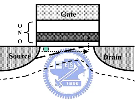
Fig. 2-4 Channel hot electron injection is used for programming. Electrons are accelerated by the high lateral electric field; gain enough energy to overcome the interface barrier, and then are trapped in the storage layer.
Si3N4
1φ
q
Si sub (p type)
(a)
Si3N4Si sub (p type) Si sub (p type) Si3N4
(b) (c)
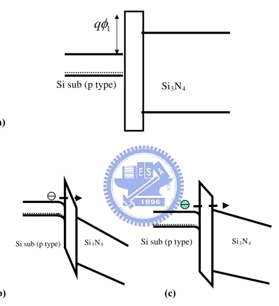
Fig. 2-5 (a) The band diagram of Si-oxide-nitride interfaces. (b) F-N tunneling occurs when Etox is larger than
tox t qφ1
. (c) Direct tunneling
occurs when Etox is smaller than
tox t qφ1
P-substrate
Gate
N
+V
G< 0
V
D> 0
Deep-depletion region(a)
Si3N4 Oxide Drain(b)
Fig. 2-6 Band to band tunneling. (a) When biasing a large negative voltage on gate electrode in an n-channel device, a deep depletion region appears in the overlap of gate and drain. (b) Holes will be attracted by the negative gate bias to tunnel into the storage nitride layer
Program state
Thr
eshol
d voltage
Fresh P/E cycled Erase stateRetention time
Fig. 2-7 Typical characteristics of threshold voltage evolution with retention time. The difference between fresh and P/E cycled devices is related to the charge trapped in the oxide and resulting in reliability degradation.
Thermionic emission Tunneling mechanism
Tunneling
oxide
Nitride
Blocking
oxide
Gate
Substrate
Fig. 2-8 Major leakage paths from storage trapping sites. One is thermionic emission and the subsequent Frenkel-Poole mechanism (solid line). Another is charge-assisted-tunneling mechanism (dashed line).
Number of P/E cycles
Threshold voltage
Program state
Fresh
P/E cycled
Erase state
HP 4156A Agilent E5250A
Agilent 8110A
Fig. 3-1 The configuration of measured setting, which includes an HP-4156A for I-V measurement, an Agilent-E5250A acting as a switch, and an Agilent-8810A acting as a pulse generator.
VD = 1V
V
G(V)
-6 -4 -2 0 2 4 6I
D(A)
10-15 10-14 10-13 10-12 10-11 10-10 10-9 10-8 10-7 10-6 10-5 SG mode TG mode DG mode SG+TGmode(a)
VD = 1VV
G(V)
-6 -4 -2 0 2 4 6I
D(A)
10-13 10-12 10-11 10-10 10-9 10-8 10-7 10-6 10-5 SG mode TG mode DG mode SG+TG mode(b)
Fig. 3-2 Transfer characteristics of (a) NW-SONOS and (b) HM -SONOS devices operated under SG mode, TG mode, and DG mode. The sum of the SG and TG modes is also shown for comparison.
Normalize to GW=0.5um VG= -4v, VD=3v
Gate Width(um)
0.0 0.5 1.0 1.5 2.0 2.5I
D/I
D( GW=0. 5 ) 0.8 1.0 1.2 1.4 1.6 1.8 SG-mode TG-modeFig. 3-3 Off-state current of NW-SONOS devices as a function of gate width.
Normalize to GW=0.5 VG= -4v, VD=3v
Gate Width(um)
0.0 0.5 1.0 1.5 2.0 2.5I
D/I
D( GW=0. 5 ) 0.6 0.8 1.0 1.2 1.4 1.6 SG-mode TG-modeFig. 3-4 Off-state current of HM-SONOS devices as a function of gate width.
SG
D A B
S TG
(a)
not gated by the side-gateSide Gate Drain Side Gate Drain Side Gate Side Gate
(b) (c)
(d) (e)
Fig. 3-5 (a) Top view of the device layout. Conduction paths for SG mode of operation with (b) large gate width and (c) small gate width, and for TG mode with (d) large gate width and (e) small gate width.
Drain Drain Gate width Gate width Gate width Gate width
step = 0.5V
V
side-gate(V)
-1
0
1
2
3
4
I
D(A)
10
-1210
-1110
-1010
-910
-810
-7 VTG = -2v VTG = 2v(a)
step=1VV
top-gate(V)
-1 0 1 2 3 4I
D(A)
10-12 10-11 10-10 10-9 10-8 10-7 VSG =-2 v VSG =2v(b)
Fig. 3-6 Measured ID-VG curves of a NW-SONOS device under (a) SG
mode of operations with various top-gate voltages, and (b) TG mode of operations with various side-gate voltages.
step=1V
V
side-gate(V)
-6 -4 -2 0 2 4 6 8I
D(A)
10-13 10-12 10-11 10-10 10-9 10-8 10-7 10-6 10-5 VTG = -2v VTG = 2v(a)
step=1VV
top-gate(V)
-8 -6 -4 -2 0 2 4 6 8I
D(A)
10-13 10-12 10-11 10-10 10-9 10-8 10-7 10-6 10-5 10-4 VSG = -2v VSG = 2v(b)
Fig. 3-7 Measured ID-VG curves of a HM-SONOS device under (a) SG
mode of operations with various top-gate voltages, and (b) TG mode of operations with various side-gate voltages.
F1-12 10-6 10-5 10-4 10-3 10-2
de
lta
Vth(
V)
0.0 0.5 1.0 1.5 2.0 2.5 3.0 P(13,0,0,0) P(14,0,0,0) P(15,0,0,0) P(13,0,0,0)HM P(14,0,0,0)HM P(15,0,0,0)HMTime(s)
(a)
Time(s)
10-3 10-2 10-1 100 101delta Vt
h(
V)
-2.5 -2.0 -1.5 -1.0 -0.5 0.0 0.5 E(-8,0,0,0) E(-9,0,0,0) E(-10,0,0,0) E(-11,0,0,0) E(-8,0,0,0)HM E(-9,0,0,0)HM E(-10,0,0,0)HM(b)
Fig. 3-8 (a) Programming and (b) erasing characteristics under various stress voltages. Black lines are measured in NW-SONOS, and gray lines in HM-SONOS.
channel oxide Si3N4 oxide gate
channel
(a)
oxide oxide Si3N4 gate
(b)
N-type gate P-type gate
(a)
Time(s)
10-3 10-2 10-1 100 101delta Vth(V)
-2.5 -2.0 -1.5 -1.0 -0.5 0.0 (-9,0,0,0) P-type SG (-10,0,0,0) P-type SG (-10,0,0,0) N-type SG (-9,0,0,0) N-type SG(b)
Fig. 3-10 (a) Schematic band diagram of NW-SONOS devices with P-type and N-type side-gate under erasing operation. Electron tunneling from the gate is effectively blocked with the P-type gate. (b) Comparisons of erasing efficiency of NW-SONOS devices with P-type and N-type side-gate.
V
side-gate(V)
-4 -2 0 2 4 6I
D(A)
10-15 10-14 10-13 10-12 10-11 10-10 10-9 10-8 10-7 Fresh state P-state (15,0,0,0) E-state (-9,0,0,0)(a)
V
side-gate(V)
-4 -2 0 2 4 6I
D(A)
1e-12 1e-11 1e-10 1e-9 1e-8 1e-7 1e-6 Fresh state Programming state Erasing state(b)
Fig. 3-11 Log-ID vs. side-gate voltage of different states in (a) NW-SONOS
V
side-gate(V)
0 1 2 3 4 5 6I
D(A)
2x10⁻¹⁰ 4x10⁻¹⁰ 6x10⁻¹⁰ 8x10⁻¹⁰ 10-9 Fresh state P-state (15,0,0,0) E-state (-9,0,0,0)(a)
V
side-gate(V)
0 1 2 3 4 5 6I
D(A
)
2x10⁻¹⁰ 4x10⁻¹⁰ 6x10⁻¹⁰ 8x10⁻¹⁰ 10-9 Fresh state P-state (15,0,0,0) E-state (-9,0,0,0)(b)
Fig. 3-12 Linear-ID vs. side-gate voltage of different states in (a) NW-SONOS
Program (15,0,0,0)
Time(s)
10-6 10-5 10-4 10-3 10-2delt
a Vth(V)
0 1 2 3 4 SG mode TG mode DG mode(a)
Erase (-9,0,0,0)Time(s)
10-3 10-2 10-1 100 101delta Vth(V)
-4 -3 -2 -1 0 SG mode TG mode DG mode(b)
Fig. 3-13 Delta Vth versus time in (a) programmingand (b) erasing operation under SG, TG, and DG modes.
Program (15,0,0,0) T=1us
V
TG -6 -4 -2 0 2 4 6 8del
ta V
th(V
)
0.0 0.5 1.0 1.5 2.0 0.0 0.5 1.0 1.5 2.0(a)
Erase (-9,0,0,0) T=1sV
TG -8 -6 -4 -2 0 2 4 6 8d
e
lta Vth(V)
-2.5 -2.0 -1.5 -1.0 -0.5 0.0 -2.5 -2.0 -1.5 -1.0 -0.5 0.0(b)
Fig. 3-14 Shift in Vth as a function of the applied top-gate voltage for NW-SONOS devices after (a) programming and (b) erasing.