行政院國家科學委員會專題研究計畫 成果報告
高介電材料結合 SONOS 之新穎非揮發性記憶體元件製作與
物理特性研究(2/2)
研究成果報告(完整版)
計 畫 類 別 : 個別型 計 畫 編 號 : NSC 98-2221-E-009-002- 執 行 期 間 : 98 年 08 月 01 日至 99 年 07 月 31 日 執 行 單 位 : 國立交通大學電子工程學系及電子研究所 計 畫 主 持 人 : 施敏 計畫參與人員: 碩士班研究生-兼任助理人員:謝介銘 碩士班研究生-兼任助理人員:張耀峰 碩士班研究生-兼任助理人員:黃志文 博士班研究生-兼任助理人員:陳仕承 博士班研究生-兼任助理人員:胡志瑋 博士班研究生-兼任助理人員:馮立偉 博士班研究生-兼任助理人員:鍾宛芳 博士班研究生-兼任助理人員:王信淵 處 理 方 式 : 本計畫可公開查詢中 華 民 國 99 年 08 月 30 日
行政院國家科學委員會補助專題研究計畫
■成果報告 □期中進度報告高介電材料結合SONOS之新穎非揮發性記憶體元件製作與物理特
性研究(2/2)
計畫類別:
■
個別型計畫 □整合型計畫
計畫編號:
NSC
98-2221-E-009-151-執行期間: 98 年 8 月 1 日至 99 年 7 月 31 日
執行機構及系所:交通大學
計畫主持人:
施敏
共同主持人:
計畫參與人員:馮立偉 胡志瑋 鍾宛芳 陳仕承 王信淵
黃志文 謝介銘 張耀峰
成果報告類型(依經費核定清單規定繳交):□精簡報告
■
完整報告
本計畫除繳交成果報告外,另須繳交以下出國心得報告:
□赴國外出差或研習心得報告
□赴大陸地區出差或研習心得報告
□出席國際學術會議心得報告
□國際合作研究計畫國外研究報告
處理方式:
除列管計畫及下列情形者外,得立即公開查詢
□涉及專利或其他智慧財產權,□一年□二年後可公開查詢
中 華 民 國 99 年 8 月 11 日
行政院國家科學委員會補助專題研究計畫成果報告
高介電材料結合SONOS 之新穎非揮發性記憶體元件製作與物理
特性研究(2/2)
執行期限:98 年 8 月 1 日至 99 年 7 月 31日
計劃編號: NSC 98-2221-E-009-151-
計劃主持人: 交通大學電子工程學系及電子研究所 施敏 教授
1.中文摘要 近年來,傳統的浮動閘極非揮發性記 憶體結構,在隨著元件微縮化、穿隧 氧化層隨縮, 勢必面臨到資料保存上 的挑戰。因而透過氧化矽-氮化矽- 氧 化 矽 (oxide-nitride-oxide,ONO) 及 利用量子奈米點作為儲存層相繼被提 出,這兩種結構被認為是非揮發性記 憶體元件下一個世代,其中SONOS 結 構是利用氮化矽取代浮動閘極作為記 憶體元件之儲存層,利用氮化矽中的 缺陷作為隔絕性的儲存中心,改善浮 動閘極微縮後資料容易因為穿隧氧化 層劣化而遺失,以解決資料無法長時 間保存的問題。本計畫中,我們將針 對現今的SONOS 結構做進一步的提昇 並 進 行 物 理 機 制 上 的 討 論 。 在 第 一 年,我們將透過改變不同材料,利用 高介電係數材料取代傳統二氧化矽作 為穿隧氧化層、阻障氧化層或是儲存 層,除了建立完整的高介電係數材料 薄膜沉積資料庫外,並透過對元件做 完整之電性研究,討論其材料改變所 造成的影響,以建立完整的物理模型 釐清載子儲存機制及傳輸原理,希望 透過改變材料得到提升傳統SONOS元 件結構的效能。在第二年,我們將著 重於記憶體元件的完整製作,透過改 變傳統的MOSFET 結構,如利用奈米線 通道等方式,以期能夠提升SONOS 記 憶體元件的寫入抹除效率,也透過完 整 的 電 性 量 測 , 萃 取 相 關 的 特 性 分 析,如缺陷密度等。 關鍵詞:非揮發性記憶體;氧化矽-氮 化矽-氧化矽;高介電係數材料 1-1.英文摘要In recent year, the traditional floating gate memory devices face a challenge about data retention with the device size scaling down and tunneling oxide thinning. Hence, using the oxide-nitride-oxide (ONO) and the nanodots structure to be the trapping layer was proposed sequentially. These structures are thought to be the next generation of the nonvolatile memory devices. The SONOS memory devices store the data by trap the charges in the trap-rich nitride. The stored charges are not lost because the isolation of the trapping sites in nitride. Even if the
tunneling oxide is degraded, the data retention is improved. In this project, we will enhance the performance of the SONOS devices and discuss the physical models of the data storage. In the first year of the project, we will replace silicon oxide with the high-k materials to be the tunneling oxide, blocking oxide or trapping layer. Besides establishing the data base of the deposited high-k thin films, the electrical effects of high-k materials will also be studied using CV, IV and DLTS technology of measurement. In addition, the whole physical models of charge trapping and the mechanisms of carriers transport will be defined to enhance the performance of SONOS memory devices. In the second year of the project, we will focus on the whole fabrication of the Metal-Oxide-Silicon Field Effect Transistor (MOSFET) structure. The program and erase efficiency will be improved by the changes of the device structure such as use the nanowires to be the channel of the device. Additionally, we also extract the electrical characteristics of the memory devices through whole electrical measurement. Keywords:Nonvolatile Memory, ONO, High-k
2. Introduction
Today, non-volatile memory (NVM) devices attract much attention as the requirements of portable products increase. However, a dry oxidation process, which is above 900 ℃, is the most common fabricating process to form the memory tunneling oxide. Applications of the current NVM are limited because the devices need a high-quality thermal oxide as the tunneling oxide to assure the charge-storage ability after a long duration operation. In order to low the
fabricating temperature, low-temperature oxide deposited
technologies will be critical for the next generation NVM. Several methods had been proposed to form a high-quality oxide at lower temperature such as the electron beam gun evaporation, atomic layer deposition and the supercritical-fluid treatment. However, aforesaid methods need an expensive instrument or have a throughput issue. Recently, nitric acid oxidation has been confirmed as a novel and attractive method to form a thin and high quality oxide at low temperature. We also believe that the nitric acid oxidation technology is also effective to form the NVM tunneling oxide. In addition, previous studies have shown the nanocrystals (NCs) devices need enough energy to help the NCs to aggregate. It is disadvantageous to apply the NCs if the NCs need a higher fabricating temperature. Self-assembled method to
form NCs indicates that the aggregation of NCs depends on the initial nuclei formation and NCs growth rate. It had been proposed about the method to enhance the NCs aggregation through diffusing the additional elements to form more nucleation centers. Moreover, we believe that the similar idea that the nucleation process improved by the internal elements of the self-assembled layer can also enhance the NCs formation. In our project, we want study the possibility for the Al2O3 film, which
is prepared by the nitric acid oxidation method, is used to be the tunneling oxide of CoSi2 nanocrystals (NCs)
memory device. Also, the metal-insulator-silicon (MIS) structure was fabricated to test the quality of the formed Al2O3. Then, we deposited the
self-assembled CoSi2 film to be the
trapping layer of the memory device. After the fabrication of the metal-oxide-insulter-oxide-oxide
(MOIOS) structure, the charge-storage ability of the NCs memory devices with the nitric acid oxidized Al2O3 as the
tunneling oxide has been discussed by the material and electrical analyses. Moreover, we want to find the extra material to form the trapping layer of memory devices such as a high-k material or novel NCs. Then, we proposed the novel NCs memory structure fabricated by annealing the Ni, Si and Ge mixed (NiSiGe) film. After a RTA process, it is found that the annealed NiSiGe film showed a higher
NCs size and density distribution than the conventional NiSi NCs obviously. X-ray photoelectron spectroscopy (XPS), Raman spectroscopy and energy dispersive spectrometer (EDS) were used to confirm that the large size and high density NCs is because that the internal Ge elements provide the additional nucleation centers and enhance the NCs formation. In addition, the excellent electrical characteristics of NiSiGe NCs memory device have also been demonstrated.
3. Results and Discussion-
(3.1 The Al2O3 formed by nitric acid
oxidation method) 3-1-1 (Experiment)
The experiment was started with a sputtering process to form a about 2-nm-thick pure Al film on p-type (100) Si wafer which had been removed native oxide and particles by RCA process. Afterward the Al film was immersed in nitric acid solution (HNO3:H2O= 1:10)
for 60s at room temperature to form the Al2O3 film. Portion of the samples were
fabricated to be the metal-insulator-silicon (MIS) structure to test the quality of the formed Al2O3. Then, we also formed the memory devices by the sputtering system to deposit an about 6-nm-thick CoSi2 film
as self-assembled trapping layer. Subsequently, a rapid thermal annealing (RTA) set at 700 °C was performed for 30s in N2 ambient to form CoSi2 NCs
structure and improve the quality of the
Al2O3 film. After the RTA process, a
50-nm-thick blocking oxide (SiO2) was
capped by plasma enhanced chemical vapor deposition system. Finally, the top and bottom Al electrode was patterned to form the MOIOS structure. After the fabricating of the NCs memory device, transmission electron microscopy (TEM) and X-ray photoelectron spectroscopy (XPS) was used to analyze the compositions of the Al2O33 and CoSi2
NCs. Furthermore, the electrical measurements such as capacitance-voltage (C-V), current density-voltage (J-V), retention and endurance measurements were used to investigate the charge-storage ability of the formed NVM device.
3-1-2 (Discussions)
2HNO3 Æ 2NO+H2O+3O (1)
Fig. 1 (a) C-V result of the MIS (b) cross-section TEM images of the formed CoSi2 nanocrystals memory device.
The oxidation mechanism is the decomposition of HNO3 provides a high
concentration of atomic oxygen to oxidize the Al film. Hence, the oxidation can be accomplished by the brief immersion. Additionally, the aggregation of the CoSi2 NCs is
indicated by the appearance of peak at 778.3 eV as shown in Fig.2 (c). During the 700 ℃ annealing process, the deposited CoSi2 film tends to aggregated
by minimizing the surface energy and relaxing the interface stress. Then, the CoSi2 NCs attribute the charge-storage
sites for the memory application. Figure 1 demonstrates the C-V MIS
structure. It is found the nitric acid oxidized Al2O3 (after only 400 ℃ RTA
process) shows a negligible hysteresis phenomenon at ±3V gate voltage operation as shown as the Fig.1(a). The electrical results confirm that the quality of the Al2O3 is excellent even the oxide
was formed by the brief nitric acid immersion and RTA process. Figure 1 (b) is the cross-section TEM images of the formed CoSi2 NCs memory device.
After the 700 °C RTA process, it is found the Al2O3 formation and CoSi2
NCs aggregation obviously. The formed Al2O3 film is about 4~5nm and the
CoSi2 NCs are about 5nm, respectively.
The 700℃ rapidly annealing is used to promote the CoSi2 NCs to aggregate. In
addition, the quality of the nitric acid oxidized Al2O3 also can be further
improved through the annealing. In order to confirm the Al2O3 formation
and NCs aggregation, XPS analysis was used. Fig. 2 (a)~(c) shows the XPS results of the tunneling oxide and trapping layer. In the result of Al 2p XPS analysis (Fig.2 (a) and (b)), it is found that only a binding energy is found at ~75 eV, reported by the previous literature indicated as Al-O binding. It is believed that the deposited Al film is effectively oxidized after the brief nitric acid immersion according to the chemical equation (1).
Fig. 3 (a) Memory effect obtained from C-V haracterization and (b) current density easurement of the formed CoSi2 NCs memory evice.
Figure 3 shows the C-V and J-V easurement for the CoSi2 NCs memory
evice. The bidirectional C-V sweeps ere performed from deep inversion to eep accumulation and in reverse, which exhibited a flat-band voltage (VFB) shift, indicating charge-storage ability of the NCs. In Fig. 3(a), it is found that the CoSi2 NCs memory device shows a
memory window of 5V under ± 10 V gate voltage operation. The formed Al2O3 can hold the charge in the NCs
instead to lose into the Si-sub. In addition, the J-V result indicates as shown Fig.3 (b) indicates the low-temperature deposited Al2O3
without serious leakage current is potential for the application of the tunneling oxide.
Fig. 2 The XPS results of the tunneling oxide ((a) s-deposited and (b) after RTA process) and rapping layer (c) of the memory device.
3-1-3 (Conclusion)
In conclusion, an Al2O3 film formed by
the nitric acid oxidation is proposed to be the tunneling oxide for the CoSi2 NCs
memory device in this work. Material
and electrical results assure the Al film can be oxidized completely after immersing the nitric acid solution. By the fabricating the MOIOS structure, the formed CoSi2 NCs memory reveals an
excellent memory effect. A lower temperature but high-quality Al2O3 film
is advantageous to improve the thermal budget issue for the thermal oxide demand of the conventional NCs memory devices.
5
(3.2 NiSiGe nanocrystals for nonvolatile memory devices)
3-2-1 (Experiment)
The fabrication of memory structure was started with a dry oxidation at 950 °C to form a 5 nm-thick tunneling oxide on p-type (100) Si wafer which had been removed native oxide and particles by RCA process. Afterward a 6-nm-thick NiSiGe thin film was deposited by co-sputtering the NiSi2 and Ge targets,
simultaneously. Then, a 20-nm-thick capped oxide was deposited to form a tri-layer structure by plasma enhanced chemical vapor deposition (PECVD). Subsequently, a rapid thermal annealing (RTA) at 600 °C was performed for 30s in N2 ambient to form NCs structure. After the RTA process, a 30-nm-thick blocking oxide (SiO2) was capped by
PECVD system. Finally, Al gate electrode was patterned to form MOIOS structure. In addition, the structure with NiSi NCs was formed by the same process for comparison. Transmission electron microscopy (TEM), Raman spectroscopy, XPS and EDS were used
to analyze the NCs formation. Related electrical measurements such as capacitance-voltage (C-V), retention measurement were used to study the charge-storage ability of the NCs memory devices.
3-2-2 (Discussions)
Figure 4 shows the plane-view and cross-sectional TEM images of the NiSi [Figs. 4(a) and 4(c)] and NiSiGe [Figs. 4(b) and 4(d)] layer after thermal annealing process. After the 700 °C RTA process, it is found that the NiSi NCs aggregated at the tunneling oxide obviously. The size and density of the NCs (>2nm) calculated from the plane-view TEM is about 2~3nm and 3.02×1011 cm-3, respectively. In addition, the aggregation of the NiSiGe NCs also can be found in annealed NiSiGe film (600 °C).
Fig. 4 The plane-view and cross-section TEM micrographs of the annealed NiSi (a&c) and NiSiGe (b&d) film.
It is confirmed the NiSiGe NCs, which is about 8~10 nm and 4.95×1011 cm-3,
reveal a better NCs growth process than the NiSi NCs. We think that the internal Ge of NiSiGe film play an important role for the NCs improvement because the internal Ge elements of NiSiGe film can provide additional nucleation centers and low the NCs formation temperature. An early nuclei formation brings the enhancement of the NCs size and density.
Fig. 5 (a) The Ge 3d XPS spectra, (b) Raman spectroscopy and (c) EDS of the NiSiGe film after the thermal annealing. In order to confirm the attribution of the Ge elements during the NCs formation process, the related material analyses was used. In the result of Ge 3d XPS analysis, a binding energy is found at ~31.5 eV, reported by the previous
literature indicated as nickel-germane-silicide (Ni-Si-Ge) binding. Additionally, the appearance of peak at 29.4 eV means the precipitation of the Ge. Fig.5 (b) is the Raman spectra of the annealed NiSiGe samples. It can be seen that for the annealed NiSiGe film, there is a broad peak at about 220 cm−1, corresponding to the Ni-Si-Ge
phase. Whereas a Ge-Ge peak peaks at about 300 cm−1, was found at 600 °C thermal annealed samples. Also, the EDS analysis was used to analyze the compositions of the NCs. The electron beam was focused at the NCs region about 10nm during the EDS analysis. We found that the NCs composed with Ni, Si and Ge elements. Through the results of the material analyses, it is believed that the main composition of the NCs is not pure NiSi2 because the
Ge can be the initial nucleation centers to form the NCs. According the reported literature, the Ge elements tend to precipitate during the thermal annealing. Compared with the NiSi mixed film, the NiSiGe layer offers more additional nucleation centers for the NC formation. Therefore, the NiSiGe film can provide a more complete nucleation process and induce a higher size and density distribution at lower fabricating temperature.
Fig.6 High-frequency C–V characteristics of the MOIOS structures: (a) with NiSi NCs and (b) NiSiGe NCs as the trapping layer of the memory device.
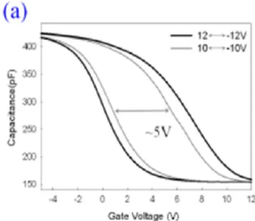
Figure 6 shows the C-V hysteresis after bidirectional sweeps, which implies
electron charging and discharging effect of the MOIOS structure. In Fig. 6(a), the conventional NiSi NCs memory device shows flat-band voltage (VFB) shift of 4.5V under ± 10 V gate voltage operation. In contrast to the NiSi NCs, the NiSiGe NCs memory device exhibits 9V flat-band voltage shift in Fig. 6(b). The larger window of NiSiGe NCs due to the improved NCs formation is advantage to be defined as “1” or “0” for the logic-circuit design.
7
Fig. 7 Retention characteristic of the (a) NiSi and (b) NiSiGe NCs memory device.
Figure 7 shows the retention characteristic of (a) NiSi NCs and (b) NiSiGe NCs device. It is found that the NiSiGe NCs device reveals better charge-storage ability than the NiSi NCs after 104 sec. The better retention characteristic is because the NiSiGe NCs have lower quantum confinement effect due to the larger NCs size distribution. Also, it is confirmed the Ge elements of the NiSiGe film did not damage the tunneling oxide quality.
3-2-3 (Conclusion)
In conclusion, we demonstrate the NiSiGe NCs memory device formed by annealing the NiSiGe film. It is confirmed the Ge element of NiSiGe
film can offer more nucleation centers and enhance the NiSiGe NCs formation by the related material analyses. Evan at lower annealing temperature, the NiSiGe film obtains larger NCs size and higher density distribution. Furthermore, the NiSiGe NCs memory device shows superior charge-storage ability to the conventional NiSi NCs due to the improved NCs formation process. The good retention characteristic of NiSiGe NCs device is also advantageous to apply into the current memory fabricating process.
(3.3 Nitric Acid Oxidation of Si for the Tunneling Oxide Application on CoSi2
Nanocrystals Nonvolatile Memory) 3-3-1 (Experiment)
Fig. 1 The process flow proposed in this work.
Figure 1 is the process flow of the experiment. The fabrication of the memory structure started with a sputtering process to form a Si thin film about 2 nm thick on a p-type (100) Si wafer, from which native oxide and particles had been removed by the RCA process. Then, the Si film was immersed in nitric acid solution (HNO3:H2O =
form the NAO-SiO2 layer. Portions of
the NAO-SiO2 were fabricated to be the
MIS structure. In addition, a 6 nm thick CoSi2 film was deposited by the
sputtering system on the other portion of the samples to be the self-assembled trapping layer. Then, the samples were annealed by a rapid thermal annealing (RTA) system set at 700°C for 30 s in pure N2 ambient to form the CoSi2 NC
structure. After the RTA process, a 50 nm thick blocking oxide (SiO2) was
capped by a plasma-enhanced chemical vapor deposition system. Finally, top and bottom Al electrodes were patterned by a shadow mask to form a metal-oxide-insulator-oxide silicon (MOIOS) structure. After the fabrication of the devices, the related material and electrical analyses were used to analyze the CoSi2 NC memory devices using the
NAO-SiO2 as the tunneling oxide.
3-3-2 (Discussions)
8
Fig. 2 The (a) C-V and (b) J-V characteristics of MIS structure using the NAO-SiO2 layer as the gate oxide. The inset of (a) is the cross-section TEM image of the MIS structure.
Figure 2a and b shows the C-V and current density–voltage (J-V) characteristics of the MIS structure, respectively, using the NAO-SiO2 as the
gate oxide. In Fig. 2a, the conditions of the samples are divided as (a) without and (b) with a subsequent 700°C RTA treatment for 30 s. The C-V measurement was swept from -3 to 3 V to extract the quality of the oxide. An obvious leakage behavior at a higher gate voltage and poorer uniformity of the electrical performance can be found in the samples without the POA process. Also, an obvious (~0.5 V) hysteresis of the C-V sweep means that some charges were trapped in the NAO-SiO2 (without
POA treatment) during the measurements. Nevertheless, the hysteresis and leakage current behavior can be reduced by the subsequent 700°C annealing process. The improvement may be attributed to the decrease in defects in the NAO-SiO2 layer. We also
extract the equivalent oxide thickness (EOT) through the C-V results. The EOT of the NAO-SiO2 with RTA at 700°C
for 30 s is about 4 nm and is obtained by calculating the 88.56 pF of the accumulation capacitance in C-V curves. The result fits in with the cross-section transmission electron microscopy (TEM) image of the inset of Fig. 2a. In addition, the J-V characteristic of the MIS structure using the NAO-SiO2 (after
700°C annealing process) as the gate oxide was also measured, as shown in Fig. 2b. The highest gate leakage current of the NAO-SiO2 layer is about 10−2 A/cm2 under -2 V gate voltage operation, which is lower than the defined gate limit in the literature. The result also
Fig. 3 The Si 2p XPS spectra of (a) the as-deposited Si film and the NAO-SiO2 (b) before and (c) after the RTA set at 700°C for 30 s.
indicates that the NAO-SiO2 without serious leakage current has potential for the application of the electric device. In the J-V result, a nonsymmetric leakage behavior was obvious. The higher gate injection current density under negative gate voltage resulted from the electrons injected from the Al gate to the Si substrate. In contrast, a current saturation of the J-V characteristic is found when a positive gate bias is applied because the gate leakage current in the deep depletion region is related to the generation of minority carriers via the bulk traps and interface states in the depletion region.
Figure 3 demonstrates the Si 2p XPS spectra of (a) the as-deposited Si film and the NAO-SiO2 (b) before and (c)
after the RTA at 700°C for a 30 s process. Figure 3ashows a peak at about 99.3 eV corresponding to the Si–Si bonding energy. We found an additional peak at about 103 eV, which is attributed to the native oxide formed during the sample fabrication. After the nitric acid immersion, an obvious transition of Si elements to SiO2 shows
that most of the as-deposited Si film was oxidized by the nitric acid solution, as shown in Fig. 3b. The oxidation mechanism of the nitric acid oxidation explains that the decomposition of HNO3 can provide a high concentration
of atomic oxygen with a strong oxidizing ability to oxidize the sputtered Si film. In addition, some suboxide (SiOx,x < 2) is found in Fig. 3b, which confirms that the oxide still has a poorer quality. As an annealing temperature was used to improve the oxide quality, the Si–O peak was shifted toward higher binding energies and the suboxide element was reduced. Hence, the oxidation was accomplished by the brief nitric acid immersion and a POA treatment. To study the feasibility for the NAO-SiO2 layer to be applied to the NC
memory device, the MOIOS structure was fabricated and measured. After the
700°C RTA process, SiO2 formed and
CoSi2 NCs obviously aggregated, as
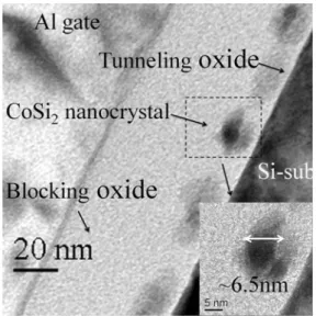
shown in Fig. 4. The formed NAO-SiO2
film of the memory device is about 4 nm and the CoSi2 NCs are about 6.5 nm.
The purpose of the 700°C rapid annealing is to promote the CoSi2 NCs to aggregate. According to the literature, an adequate external energy provided by the thermal system can induce the aggregation of the deposited CoSi2 thin
film. The total energy of the thin film is reduced when the surface area is minimized by forming a discrete and roughly spherical NC structure. Moreover, XPS analyses were used to confirm the CoSi2 NCs aggregation.
Fig. 5 The (a) Co 2p3/2 and (b) Si 2p XPS spectrum of the charge-trapping layer after the RTA at 700°C for 30 s. The EDS analyses of the compositions of the (c) NAO-SiO2 and (d) NCs.
The chemical composition of the charge-trapping layer is demonstrated in Fig. 5a and b. The main peak of 778.5 eV in the Co 2p3/2 XPS spectrum corresponding to the binding energy of the CoSi2 phase confirms that the charge
storage centers are mainly composed of CoSi2 NCs. The Co–Si signal can also
be found in the Si 2p XPS of the trapping layer, as shown in Fig. 5b. Moreover, an energy-dispersive spectrometer (EDS) was used to analyze the compositions
Fig. 4 The cross-section TEM image of the formed memory structure using the NAO-SiO2 as device tunneling oxide.
of the NAO-SiO2 and NCs, as shown in Fig. 5c and d, respectively. In Fig. 5c, the EDS of the NCs region is composed of strong Co and Si signals attributed to the self-assembled CoSi2 NCs. In addition, only Si and O elements are found in the EDS results of the tunneling oxide, revealing that the NAO-SiO2 has
enough ability to restrain the Co elements of the charge-trapping layer to
diffuse into the Si substrate even after a 700°C thermal annealing process, as shown in Fig. 5d. We also used a secondary-ion mass spectrometer (SIMS) to further study the possibility of Co contamination.
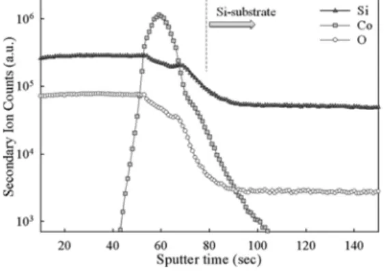
Fig. 6 The SIMS analysis of the CoSi2 NCs memory device.
Figure 6 shows the results of SIMS analysis for the CoSi2 NCs memory
device. The main Co signal only accumulated at the tunneling oxide. Hence, it is believed that the Co contamination issue of the CoSi2
memory device using the NAO-SiO2
thin film as tunneling oxide can be excluded.
11
Fig. 7 The (a) C-V and (b) J-V curve of the MOIOS structure using the NAO-SiO2 as device tunneling oxide. Figure 7a shows the high frequency (1 MHz) C-V curves of the formed CoSi2
NC memory structure. When the gate voltage of the device was swept by a ±
10 V operation, a floating-band voltage shift of 7 V was observed. The counterclockwise C-V hysteresis loops mean that the injected carrier is related to the inversion layer of the Si substrate. The obvious memory window of NC memory devices is advantageous as the judgment of the logic circuit. In addition, the J-V characteristic of MOIOS structure was also investigated, as shown in Fig. 7b. Compared with the J-V result of the MIS structure in Fig. 2b, the MOIOS structure shows a lower leakage characteristic and symmetric behavior. The result is attributed to blocking oxide, which restrains the passing charge in both the positive and the negative gate voltage modes. To study the reliability characteristics of the formed CoSi2 NC memory device,
retention and endurance characteristics were also demonstrated. The retention characteristic of the MOIOS structure was extracted by the capacitance–time measurement, as shown in Fig. 8a. The normalized capacitance, △ Cret, is defined as Eq. 1
△Cret = [C(t) − CFB]/[C(0) − CFB] (1)
where C(0), C(t), and CFB are the initial
capacitance after the programming operation, the measured capacitance during the retention test, and the referred capacitance defined at flatband voltage, respectively. The △Cret of the memory
device can be stable at about 48% of the initial capacitance after a 104 s test even with an obvious 20% capacitance drop within the first 100 s. In addition, we
demonstrate the endurance characteristic of the MOIOS structure, as shown in Fig. 8b. The endurance characteristic of the device was tested by the continuous voltage pulse set at ±10 V for 1 ms. After the continuous stress, a subsequent C-V measurement was used to examine the degeneration of the memory charge–storage ability. A slight decay in the memory window is found even after 106 cycles of pulse operations. The retention and endurance tests confirm that the memory using the NAO-SiO2 as tunneling oxide has enough reliability characteristics.
12
Fig. 8 The (a) retention and (b) endurance characteristics of the MOIOS structure using the NAO-SiO2 as tunneling oxide.
3-3-3 (Conclusion)
In summary, the nitric acid oxidation method was studied to prepare a thin oxide as the gate oxide of an electrical device. TEM and XPS results show that Si film can be oxidized completely. The process of the nitric acid oxidation and the effect of the POA were also demonstrated. The oxide quality can be improved as the suboxide element is decreased during the POA process. In addition, the CoSi2 NCs were formed as
the charge–storage centers to study the
feasibility of applying NAO-SiO2 into
the memory device. The NAO-SiO2 can
bring a memory window of 7 V under ± 10 V gate voltage sweeps. The retention and endurance tests of the formed CoSi2
NCs memory device were also demonstrated in this work. From the reported data, it is believed that the NAO-SiO2 film can provide adequate
quality and hold the stored charge during the reliability tests. Moreover, the nitric acid oxidation is easy and advantageous to improve the thermal budget issue for the current NC memory devices because the highest fabrication temperature for the improved NVM devices is only determined by the NCs. (Role of germanium in the reduced temperature dependence of Ti-based nanocrystals formation for nonvolatile memory applications)
3-4-1 (Experiment)
After a RCA clean process of a p-type silicon (100) wafer, a 4 nm thick tunnel oxide was thermally grown by a dry oxidation process. A 10 nm thick Ti-based germanosilicide layer was deposited by cosputtering with TiSi2 and
Ge targets in Argon (Ar) ambiance at a pressure of 7.6 mTorr to act as a charge tapping layer. The applied direct current powers on TiSi2 and Ge targets were
fixed at 100 and 50 W, respectively. Then, a thinner silicon dioxide layer (10 nm) was deposited by plasma enhanced chemical vapor deposition before any thermal treatments in order to reduce a possible contamination on the trapping
layer during exposure to atmosphere. Subsequently, a rapid temperature annealing was carried out at different temperatures of 400, 500, and 600 °C for 2 min to format NCs dots. After the samples were annealed, another 30 nm thick silicon oxide, i.e., a total thickness of 40 nm including the previous oxide, was deposited to act as a blocking oxide. Finally, a 500 nm thick Al gate electrode was deposited and patterned by shadow mask to form a capacitor structure. For comparison, control samples with only a 10 nm thick TiSi2 film as a trapping
layer were also fabricated in the same following conditions.
13
3-4-2 (Discussions)
FIG. 1 Shows cross-sectional TEM of the Ti-based germanosilicide samples after annealed at (a) 500 °C and (b) 600 °C.
Figure 1 shows cross-sectional transmission electron microscopy (TEM) of the Ti-based germanosilicide samples after annealed at (a) 500 °C and (b) 600 °C. Formation of NCs dots were observed in both of the samples annealed at 500 and 600 °C in Fig. 1. Nevertheless, a continuous Tibased germanosilicide film was observed to be maintained even after a 400 °C annealing treatment (not showed here).
According to the TEM results, therefore, a higher temperature treatment than 400 °C was essential to separate the 10 nm thick blanket Ti-based germanosilicide layer into NCs structures. The size of NCs also expanded to ~9 nm with a higher thermal treatment of 600 °C.
FIG. 2 (a) Shows a comparison on overall region XPS spectra between the Ti-based germanosilicide samples annealed at 500 and 600 °C. Figures 2(b)–2(d) show XPS of Si, Ge, and Ti on the samples after annealed at 500 °C, respectively.
Figure 2(a) shows x-ray photon-emission spectroscopy (XPS) spectra of overall region on the Ti-based germanosilicide samples annealed at 500 and 600 °C, detected with Ar ion milling of the 10 nm thick blocking oxide. The elemental Ti, Si, Ge peaks appeared in the sample annealed at 500 °C. However, after undergoing a 600 °C heat-treatment, the Si and Ti peaks still can be detected and nearly intact with the exception of Ge peaks, indicating thermal desorption of Ge atoms occurred severely. From the point of view of quantitative XPS analysis, the atomic
concentration ratio of Ge 2p/Ti 2p was also reduced obviously from 3.62 in the 500 °C-treated condition to 0.41 in the 600 °C-treated condition though the intensity of Ti 2p was somewhat reduced, associated with incomplete or excess milling of the blocking oxide. Decrease of Ge may be mainly caused from the production of Germanium monoxide (GeO) by oxidation of Ge during the annealing process because the GeO phase is too thermodynamically unstable to sublime at the annealing condition. This phenomenon can also be inferred somewhat from observing the decrease of contrast between NCs and SiO2 in the TEM results of Fig. 1. Peak
signals referred to Si–Si and Si–O bonds in Si 2p spectrum as well as Ge–Ge bond in Ge 2p3/2 spectrum were observed in the sample annealed at 500 °C and shown in Figs. 2(b) and 2(c), respectively. The appearance of Si–Si/Ge–Ge bonds could be related to formation of Si–Ge and contributed from the Si–Ge precipitates. In Ti 2p spectrum of Fig. 2(d), Ti–O peak signals referred to TiO2 were detected in the
sample annealed at 500 °C. It is probably due to that the trace O2 in RTA
ambiance or the absorbed O2 on the
wafer surface during wafer transportation (air exposure) induced the formation of TiO2, a thermodynamically
stable phase, during annealing process. According to the XPS results, therefore, compositions of the NCs formatted after the 500 °C annealing treatment were
confirmed as titania-germano-silicide.
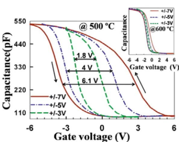
FIG. 3. And its inset show a comparison of high frequency capacitance-voltage characteristics on the Ti-based germanosilicide samples annealed at 500 and 600 °C, respectively.
Figure 3 and its inset show a comparison of high frequency capacitance-voltage characteristics on the Ti-based germano-silicide samples annealed at 500 and 600 °C, respectively. The sample annealed at 500 °C exhibited a large flat band voltage shift of ~1.8, 4, and ~6.1 V under sweeping gate voltages of 3/-3, 5/-5, and 7/-7 V, respectively. Additionally, the observed counterclockwise hysteresis loops indicated that charge carriers were injected from the silicon substrate through the tunnel oxide. However, the sample annealed at 600 °C exhibited no obvious flat band voltage shifts with gate bias voltages as shown in the inset of Fig. 3. By contrast, its control sample without Ge composition in charge trapping layer also showed no flat band voltage shifts after annealed at 500 or 600 °C (not showed here). Moreover, Ge NCs reported in past researches for
NVMs applications were almost fabricated above this temperature. Therefore, we suggest that the exhibition of large memory effect was strongly associated with the addition of Ge in Ti-based NCs, but not Ge or TiO2 NCs only.
15
FIG. 4 Shows retention and endurance
characteristics of the titania-germano-silicide NCs memory
capacitor annealed at 500 °C.
Figure 4 shows retention and endurance
characteristics of the titania-germano-silicide NCs memory
capacitor annealed at 500 °C. After the device was operated in the program/erase of +5 V/−5 V condition, the memory window retained ~0.93 V after 107 sec as well as ~3.5 V after 105 times programmed /erased cycles. 3-4-3 (Conclusion)
In conclusion, the memory effects of the titania-germano-silicide NCs fabricated by cosputtering titanium silicide and germanium targets were fabricated and demonstrated at relatively low temperature of 500 °C due to the presence of Ge atoms. The thermal desorption of Ge atoms was also observed to degrade the characteristic of
threshold voltage shift severely while further increasing the annealing temperature to 600 °C.
4. 參考文獻
[1] C. Y. Lu, T. C. Lu, and R. Liu, Proceedings of 13th IPFA, IEEE, New York, (2006), pp. 18–23.
[2] J. D. Blauwe, IEEE Trans. Nanotechnol. 1, 72 (2002).
[3] C. H. Lee, S. H. Hur, Y. C. Shin, J. H. Choi, D. G. Park, and K. Kim, Appl. Phys.Lett., 86, 152908 (2005).
[4] S. Tiwari, F. Rana, K. Chan, H. Hanafi, C. Wei, and D. Buchanan, Tech.Dig. - Int. Electron Devices Meet. 1995, 521.
[5] T. Morimoto, T. Ohguro, H. S. Momose, T. Iinuma, I. Kunishima, K. Suguro, I. Katakabe, H. Nakajima, M. Tsuchiaki, M. Ono, Y. Katsumata, and H. Iwai, IEEE Trans. Electron Devices ED-42, 915 (1995).
[6] P. X. Xu, S. R. Das, J. P. McCaffrey, C. J. Peters, L. E. Erickson, Mater. Res. Soc. Symp. Proc. 402, 59 (1995).
[7] J. D. Carey, L. L. Ong and S. R. P. Silva, Nanotechnology. 14, 1223 (2003). 10
[8] C. T. Tsai, T. C. Chang, P. T. Liu, P. Y. Yang, Y. C. Kuoand, K. T. Kin, P. L. Chang, and F. S. Huang, Appl. Phys. Lett. 91, 012109 (2007)
[9] Asuha, S. Imai, M. Takahashi, and H. Kobayashi, Appl. Phys. Lett. 85, 3783 (2004)
[10] C. S. Kuo, J. F. Hsu, S. W. Huang, L. S. Lee, M. J. Tsai; J. G. Hwu, IEEE Trans. Electron Devices 51, 854 (2004).
16
[11] T. C. Chang, P. T. Liu, S. T. Yan, and S.M. Sze, Electrochem. Solid-State Lett. 8, G71 (2005).
[12] T. C. Chang, S. T. Yan, C. H. Hsu, M. T. Tang, J. F. Lee, Y. H. Tai, P. T. Liu, and S. M. Sze, Appl. Phys. Lett. 84, 2581 (2004).
[13] P. H. Yeh, C. H. Yu, L. J. Chen, H. H. Wu, P. T. Liu, and T. C. Chang, Appl. Phys. Lett. 87, 193504 (2005).
[14] Choi, S.-S. Kim, M. Chang, H. Hwang, S. Jeon, and C. Kim, Appl. Phys. Lett. 86, 123110 (2005).
[15] Maikap, P. J. Tzeng, H. Y. Lee, C. C. Wang, T. C. Tien, L. S. Lee, and M. J. Tsai, Appl. Phys. Lett. 91, 043114 (2007).
[16] C.-H. Lin, C.-C. Wang, P.-J. Tzeng, S. Maikap, H.-Y. Lee, L.-S. Lee, and M.-J. Tsai, Jpn. J. Appl. Phys., Part 1 46, 2523 (2007)
[17] Umapathi, S. Das, K. Lahiri, and S. Kal, J. Electron. Mater. 30, 17 (2001) [18] B. Aldrich, Y. L. Chen, D. E. Sayers, R. J. Nemanich, S. P. Ashburn, and M. C. Ozturk, J. Appl. Phys. 77, 5107 (1995) 5. 計畫成果自評 本計畫今年度延續去年實驗(1)低溫 高介電係數薄膜製作並結合記憶體元 件及(2)開發新穎量子點材料儲存結 構 並 往 低 溫 化 發 展 。 在 今 年 度 計 畫 中,本實驗團隊成功研究硝酸氧化法 氧化矽薄膜形成二氧化矽之製程方法 及條件,使用於鈷矽奈米點非揮發性 記 憶 體 之 穿 隧 氧 化 層 , 建 立 完 整 之 database,而另一方面成功地加入鍺 (Ge) 於 矽 鈦 合 金 (Ti-Silicide) 為 主 之儲存層中,有效降低 Ti-base 奈米 點的製作溫度,並藉由材料分析,探 討 鍺 (Ge) 於 儲 存 層 在 退 火 中 形 成 Ti-base 奈米點所扮演之角色,與其 退火溫度與儲存窗口之關係,相關成 果已整理並逐步發表於國際期刊上。
98 年度專題研究計畫研究成果彙整表
計畫主持人:施敏 計畫編號:98-2221-E-009-002- 計畫名稱:高介電材料結合 SONOS 之新穎非揮發性記憶體元件製作與物理特性研究(2/2) 量化 成果項目 實際已達成 數(被接受 或已發表) 預期總達成 數(含實際已 達成數) 本計畫實 際貢獻百 分比 單位 備 註 ( 質 化 說 明:如 數 個 計 畫 共 同 成 果、成 果 列 為 該 期 刊 之 封 面 故 事 ... 等) 期刊論文 0 0 100% 研究報告/技術報告 0 0 100% 研討會論文 0 0 100% 篇 論文著作 專書 0 0 100% 申請中件數 0 0 100% 專利 已獲得件數 0 0 100% 件 件數 0 0 100% 件 技術移轉 權利金 0 0 100% 千元 碩士生 3 3 100% 博士生 5 5 100% 博士後研究員 0 0 100% 國內 參與計畫人力 (本國籍) 專任助理 0 0 100% 人次 期刊論文 5 5 100% 研究報告/技術報告 0 0 100% 研討會論文 0 0 100% 篇 論文著作 專書 0 0 100% 章/本 申請中件數 0 0 100% 專利 已獲得件數 0 0 100% 件 件數 0 0 100% 件 技術移轉 權利金 0 0 100% 千元 碩士生 0 0 100% 博士生 0 0 100% 博士後研究員 0 0 100% 國外 參與計畫人力 (外國籍) 專任助理 0 0 100% 人次其他成果
![Figure 4 shows the plane-view and cross-sectional TEM images of the NiSi [Figs. 4(a) and 4(c)] and NiSiGe [Figs](https://thumb-ap.123doks.com/thumbv2/9libinfo/8760690.208104/9.892.469.770.693.973/figure-shows-plane-cross-sectional-images-nisi-nisige.webp)