國 立 交 通 大 學
平面顯示技術碩士學位學程
碩士論文
非極性氮化鎵量子井結構與發光二極體元件特性研究
Investigation and characterization of nonpolar GaN
quantum-well structures and light-emitting diodes
研究生:張寶曜
指導教授:郭浩中 教授
非極性氮化鎵量子井結構與發光二極體元件特性研究
Investigation and characterization of nonpolar GaN quantum-well
structures and light-emitting diodes
研究生: 張寶曜 Student: Bao-Yao Chang 指導教授:郭浩中 教授 Advisor: Prof. Hao-Chung Kuo
國 立 交 通 大 學
平面顯示技術碩士學位學程
碩 士 論 文
A Thesis
Submitted to Degree Program of Flat Panel Display Technology National Chiao Tung University
in Partial Fulfillment of the Requirements for the Degree of Master of Science
in
Program of Flat Panel Display Technology March 2010
非極性氮化鎵量子井結構與發光二極體元件特性研究
研究生:張寶曜 指導教授: 郭浩中教授 國立交通大學平面顯示技術碩士學位學程摘要
本論文中,我們利用有機金屬氣相沉積磊晶技術成長不同厚度之非極性"a" 平面氮化銦鎵/氮化鎵多重量子井作為研究對象。我們利用光激發螢光(PL)光譜 技術進行樣品的光學特性分析。 在室溫PL實驗中,顯示了非極性氮化銦鎵/氮化鎵多重量子井的內建電場並 不影響其位能,且其發光強度隨著量子井厚度由3奈米增加到12奈米而減弱。除 此之外,變溫PL實驗顯示了一個較明顯的載子侷限效應(localization effect) 存 在 於 量 子 井 較 厚 的 樣 品 中 。 成 長 非 極 性 結 構 的 另 一 優 勢 在 於 極 化 發 光 (polarized light emission)的價值,我們所測得的發光極化率大約在60%左右。另外,我們也成功成長了非極性氮化銦鎵/氮化鎵綠光發光二極體,並且探 討相關的元件特性。我們所測得的發光極化率大約在67.4%左右。此外,電激發 光頻譜顯示,當注入電流增加至20 mA時,光譜有藍位移的現象產生。此現象可 能由於能帶填充效應所致,其後隨著注入電流的增加,發光波長則維持不變。此 非極性綠光發光二極體之順向電壓大約為3.43 V,微分串聯電阻在20 mA時大約 為24歐姆,注入電流在100 mA時,光輸出功率約為240 W。
Investigation and characterization of nonpolar GaN quantum-well
structures and light-emitting diodes
Student : Bao-Yao Chang Advisor: Prof. Hao-Chung Kuo
Degree Program of Flat Panel Display Technology
National Chiao Tung University
Abstract
In this thesis, a-plane InGaN/GaN multiple quantum wells with different widths from 3 to 12 nm were grown on r-plane sapphire by metal organic chemical vapor deposition for investigation. We utilized photoluminescence (PL) technique to investigate the optical characteristics of our samples.
The PL experiments revealed that the PL emission intensity would decrease with increasing the well width of the samples from 3 to 12 nm. Meanwhile, the power dependent PL measurement indicated no apparent emission peak shift for all samples due to no built-in electric field in a-plane MQWs. Moreover, the temperature dependent PL reveals that a more apparent localization effect exist in the sample with a thicker well width which is most likely due to more serious indium fluctuations or worse crystalline quality in the MQWs. In-plane polarization effect of a-plane InGaN/GaN MQWs emission was also investigated, which pointed out an average
polarization degree ρ from our samples is about 60%.
Furthermore, we have successfully grown a-plane green light-emitting diodes on r-plane sapphire and investigated the device characteristics of a-plane green LEDs. The apparent emission polarization anisotropy was observed and the polarization degree was as high as 67.4%. In addition, the electroluminescence (EL) spectra first revealed a wavelength blue-shift with increasing drive current to 20 mA, which could be attributed to the band-filling effect, and then the EL peak become constant. The current–voltage curve showed the forward voltage of a-plane LED grown on r-plane sapphire substrate was 3.43 V and the differential series resistance was measured to be about 24 as 20-mA injected current. Furthermore, the output power was 240 W at 100-mA drive current. These results should provide a useful guidance for fabrication of light emitting devices using a-plane InGaN/GaN MQW structures.
致謝
在這兩年的學習研究生活中,課業與工作之間的協調是相當重要的。
我雖然失去少部分的休閒時間以及與家人相處快樂時光,但是我在上
課及研究時所獲得的相關知識,卻讓我對LED有更進一步的認識;而
不是只有MOCVD設備而已;在專班的學習過程中,我首先要感謝我的
指導教授 郭浩中教授,由於他的指導與隨時隨地的協助,讓我十幾
年來的設備經驗加入實際的磊晶實驗,更加奠定了從設備所看不到的
盲點,加速問題解決的速度。此外王德忠博士讓我參與他的實驗也讓
我的設備實務經驗得到驗證。而柯宗憲博士對於我的基礎觀念的不吝
指正,以及一次又一次的實驗解說,讓我更快速的釐清盲點。還有準
博士陳俊榮學長,這兩年時間的鼎力協助及指正,讓我更加明白本實
驗室的研究精神所在。通時我也感謝所有本實驗室的學長及同學,因
為我是在職專班的包容與協助,讓我得以順利的完成此一論文之研
究。當然,我也感謝佳霖科技長官們及所有同事們幫忙分擔壓力之
下,讓我可以心無旁騖的專心研究。最後,我對於母親、老婆及小孩
的一路鼓勵及精神相伴,讓我堅持到了最後,獻上我最由衷的感激。
Content
摘要...i
Abstract ………ii
致謝……… iv
Content………..v
List of tables ………vii
List of figures……….viii
Chapter 1 Introduction
1.1 The development of polar and nonpolar III-Nitride nanostructures…….….11.2 Motivation ……….………..4
Chapter 2 Characteristics of nitride-based quantum wells
2.1 Quantum confinement effect in quantum wells………..………62.2 The localization effect in InGaN/GaN quantum wells …….………8
2.3 The concept of nonpolar quantum wells……….…..9
2.4 Light polarization effect in nonpolar quantum wells………11
Chapter 3 Metalorganic Chemical Vapor Deposition System
3.1 Introduction...………..………143.2 MOCVD Reactor... …….………15
3.3 In-Situ Reflectance Monitoring During III-Nitrides Growth……….…..17
Chapter 4 Optical properties of a-plane InGaN/GaN MQWs
4.1 Sample growth and fabrication………...………284.2 Photoluminescence properties………32
4.3 Temperature-dependent Photoluminescence…...………40
4.4 In-plane polarization effect…….………49
4.5 Summary……….………54
Chapter 5 Characteristics of a-plane InGaN/GaN Green LEDs
5.1 Introduction………555.2 Sample growth and fabrication……….56
5.3 Experimental results and discussion………57
5.4 Summary………65
Chapter 6 Conclusion and Future Work
6.1 Conclusion………..…………666.2 Future work………67
Reference……….68
List of tables
Table 4.1.1 The HRXRD measured layer thickness and composition……….31 Table 4.3.1 The fitting results of activation energy for the a-plane InGaN/GaN MQWs with different well width……….47
List of figures
Fig. 1.1.1 The planar relation and orientation in hexagonal crystal structure…….3 Fig. 2.3.1 A schematic energy band diagram of (a) nonpolar quantum well and (b) polar quantum well under QCSE. ………..13 Fig. 3.2.1 Schematic reactor of production scale EMCORE D180 MOCVD system. ………22 Fig. 3.2.2 Schematic reactor of production scale AIXTRON 2600G3 HT MOCVD
system………..23 Fig. 3.2.3 Layout of the AIXTRON 2600G3 HT susceptor in the 242 inch
configuration………24 Fig. 3.2.4 photo of the reactor chamber of the AIXTRON 2600G3 HT in the 242
inch configuration………25 Fig. 3.3.1 Hardware configuration of EpiTune II for planetary reactor…………..26 Fig. 3.3.2 In-situ reflectometry for an InGaN MQW growth run………27 Fig. 4.1.1 A schematic drawing of sample structure………30 Fig. 4.1.2 The specific crystallographic index used in the HRXRD analysis………30 Fig. 4.1.3 (a)(b)(c)(d) Experiment and simulation results of HRXRD ω-2θ scans for
a-plane InGaN/GaN MQWs……….……….31 Fig. 4.2.1 The setup of PL system………..……….36 Fig. 4.2.2 (a) Room temperature PL spectra of a-plane InGaN/GaN MQWs with well
width ranging from 3 to 12 nm. (b)(c) Normalized PL energy peak and intensity plotted as a function of quantum well width………..37 Fig. 4.2.3 PL spectrum as a function of the excitation power for a-plane InGaN/GaN
MQWs with different well width………..38 Fig. 4.2.4 The relation between PL intensity and excitation power density for a-plane InGaN/GaN MQWs with different well width. ……….39 Fig. 4.3.1 PL spectra as a function of temperature from 20K to 300K for a-plane
InGaN/GaN MQWs with different well width………..45 Fig. 4.3.2 Normalized integrated PL intensity as a function of 1/T for the a-plane
Fig. 4.3.3 PL peak energy position as a function of temperature for a-plane InGaN/GaN MQWs with different well width………48 Fig. 4.4.1 The wurtzite GaN unit cell and the definition of crystal axes……….51 Fig. 4.4.2 μ -PL spectra of the a-plane InGaN/GaN MOWs for polarization angles
between 00 and 3600 in steps of 150………51 Fig. 4.4.3 Normalized μ -PL intensity versus the in-plane polarization angle for the a-plane InGaN/GaN MOWs with different well width……….52 Fig. 4.4.4 Normalized μ -PL spectra for E//c (900) and E⊥c (00) for the a-plane
a-plane InGaN/GaN MOWs with different well width………..53 Fig. 5.3.1 XRD -2 scans for the InGaN–GaN MQWs grown on the a-plane GaN
template………61 Fig. 5.3.2 (a) Room-temperature EL spectra with pulse bias for a-plane green LED. (b)
EL peak emission shift as a function of pulse current. Inset shows the image of a-plane LED chip lightened at 20-mA drive current…………62 Fig. 5.3.3 Output power and EQE as a function of drive current. Inset shows the I-V
characteristic of green LED under forward bias………63 Fig. 5.3.4 Variation of EL intensity with angular orientation of the polarizer at 20-mA
Chapter 1 Introduction
1.1 The development of polar and nonpolar III-Nitride nanostructures
In the past, a lot of process had been made in developing high-quality III-nitride electronic and optoelectronic devices. To date most of the reported laser diodes (LDs) and light-emitting diodes (LEDs) were grown on sapphire、6H-SiC、or free standing GaN substrates in the [0001] orientation. In such configuration, the [0001] polar axis, resulting from the non-centrosymmetric nature of the wurtzite phase, is aligned along the growth direction. Hence, polarization discontinuities exist along the growth direction and create fixed sheet charges at surfaces and interfaces. The total polarization of III-nitride film consists of spontaneous and piezoelectric polarization contributions. These resulting internal electric fields would bend the potential band and spatially separate electron and hole wavefunctions in potential wells which further reduce the overlap degree of them. Thus, reduced carrier recombination、 red-shift emission and decreased internal quantum efficiency are caused. These effects are manifestations of the quantum confined Stark effect (QCSE) and have been thoroughly analyzed for GaN/(Al,Ga)N quantum wells. [1, 2]
Now, nonpolar growth is a promising means of elimination the strong polarization-induced electric fields exist in wurtzite nitride semiconductors because the polar c-axis lies in the QW plane. In a word, it is a way through choosing substrate
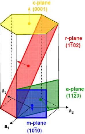
of different orientation to grow nanostructures that have no polarization electric field along growth direction in nature. There have been several approaches to realize nonpolar nanostructure, the most common two approaches are growing [1100] oriented m-plane heterostructures on γ-LiAlO2 (100) [34] and [11
20] oriented a-plane heterostructures on r-plane sapphire. [57] Planar relation and orientation in hexagonal crystal structure is shown in Fig. 1.1.1. So far, nonpolar structure has been applied to grow AlGaN/GaN and InGaN/GaN heterostructures.
Although the optical characteristics of polar c-plane heterostructures have been studied extensively [8, 9], there are still lots of optical properties of nonpolar heterostructure worth research for assistance of fabrication high efficiency optoelectronic devices. A rash of efforts have been put into nonpolar structure growth approaches and optical properties researches in these years [1013]. In this thesis, the optical characteristics and carrier recombination mechanisms of well-width dependent a-plane InGaN/GaN multiple quantum wells will be discussed. Furthermore, the characteristics of a-plane InGaN/GaN green light-emitting diodes grown on r-plane sapphire substrates are investigated as well.
1.2 Motivation
Conventional polar (c-plane) InGaN/GaN MQWs have been widely used as active layers for high brightness light-emitting diodes and continuous-wave laser diodes. But one of the most difficult challenges to improve the operation efficiency is its internal electric field as described in section 1.1. Since the non-polar QW band profiles are claimed that unaffected by internal fields, higher internal quantum efficiency and lower threshold current devices are fervently expected. Furthermore, the QCSE significantly influences the recombination efficiency of green InGaN LEDs due to the larger internal electric field induced by lattice mismatch between GaN barrier and InGaN QWs. Therefore, it can be expected that the nonpolar GaN is more necessary for Green LEDs.
Theoretically, nonpolar a-plane InGaN/GaN MQWs have potential ability to overcome the QCSE existed in polar systems and to greatly improve device efficiency. However, so far carrier recombination mechanisms and optical characteristics about them are not yet understood well. Thus, in this thesis, we put our efforts to study the optical characteristics of nonpolar a-plane InGaN multiple quantum wells grown on r-plane sapphire by metal organic chemical vapor deposition (MOCVD). Samples with different well thickness ranging from 3 to 12 nm were prepared for comparison. A series of optical experiments were applied not only to get the relations between well
width and emission characteristics but also to suggest a probable effect during the growth process of different well width of InGaN/GaN MQW. Furthermore, the growth and fabrication of nonpolar a-plane InGaN/GaN green LEDs will be discussed as well in this thesis.
Chapter 2 Characteristics of nitride-based quantum wells
2.1 Quantum confinement effect in quantum wells
If we make very small crystals, the optical properties of solids will depend on their size. The size dependence of the optical properties in very small crystals is a consequence of the quantum confinement effect. What "Quantum confinement" means is that when electrons and holes in a semiconductor are restricted in one or two or even three dimensions. For exemple, a quantum dot is confined in all three dimensions, a quantum wire is confined in two dimensions, and a quantum well is confined in one dimension. Therefore, quantum confinement occurs when one or more of the dimensions of a nanostructure is very small so that it approaches the size of an exciton in bulk crystal, called the Bohr exciton radius [14]. In this thesis, we talk about quantum well structure which is a structure where the height is approximately the Bohr exciton radius while the length and breadth in the other two dimensions are relatively free from constraint.
The distance between the electron and the hole is called the effective Bohr radius, aB of the exciton. When the well width is much larger than aB in bulk, the exciton
binding energy will not show evident difference between the well and the bulk, for the excitons feel nearly the same environment as in bulk. As the well width is decreased to the order or less than the order of a , the wave functions of electrons and holes
overlap get improved and are confined in the well. This also improves the exciton binding energy.
The Hamiltonian describing the relative motion of the exciton could be written as
H=He(xe)+Hh(xh)+He-h(r)
where He and Hh are the Hamiltonian describing the electron and hole motion
confined in the well. He-h is theHamiltonian includes the kinetic energy part of the
relative motion of the exciton in the Y-Z plane and the Coulomb potential attracting the electron and the hole in the three dimensional form. The x-coordinate of the electron and hole is denoted as xe and xh while r represent the relative position vector
between the electron and the hole. Therefore the eigenvalue solved is given by En= Eexn +Ehxn-Ee-h
where Eexn andEhxn is the energy of nth quantum confined state, and Ee-h is the binding
energy of exciton defined as positive value. Therefore, the lowest exciton resonance energy associated with the ground state in the quantum well could be written as Eemission = Eg+ Eexn +Ehxn-Ee-h
The resonance energy was sensitive to well width and the monatomic well size fluctuation in the narrower well. The well width dependence of the absorption spectra is determined by competition between the quantum confinement energy level and the
exciton binding energy.
2.2 The localization effect in InGaN/GaN quantum wells
Quantum wells based on InGaN and GaN grown on c-plane sapphire have been actively studied over the past several years for light emission. It has been seen that in spite of the substrate mismatch related high dislocation densities, the nanostructures still have reasonable quantum efficiencies in these quantum wells. In conventional light emitters, such a high density of dislocations would severely degrade the radiative efficiency. It is widely accepted that the high luminescence efficiency of polar InGaN-based structures is due to the exciton localization effect [15, 16]. Exciton localization effect is thought from a lot of reports to be induced by compositional fluctuation and phase separation observed in InGaN layers [17, 18]. Furthermore, the exciton localization effect is influenced by quantum well thickness, indium content and doping level.
Once the clusters like In-rich QD due to compositional fluctuation and phase separation formed in InGaN/GaN quantum wells, they would cause appreciable localization of the electron and hole wavefunctions. As a result of a very high degree of localization, electrons and holes injected into the InGaN quantum well are unable
to reach dislocations. This causes high radiative emission efficiency as most carriers are tapped well in localization states. The effect of indium segregation in InGaN is described by a ratio that indicates the degree of variation of In content in a cluster from pure InN cluster case. A small amount of clustering is able to provide a sufficient number of localized states for this purpose. In absence of such clustering, the carrier wavefunctions are extended into the dislocations.
2.3 The concept of nonpolar quantum wells
It was from 1994, the use of InGaN/GaN double heterostructure (DH) in LEDs by Nakamura is thought to reignite the III-V nitride system. People did a lot of work in all aspects to improve the light emission efficiency including the material selection、crystal growth、device manufacture process etc. One of the difficulties hampering further advances in nitride emitters is the presence of large piezoelectric fields in these materials.
InGaN/GaN multiple quantum wells are a widely used material and structure to serve as the active layer in nitride heterostructures for its advantage in easy tuning wavelength through controlling the composition of indium. However conventional InGaN/GaN quantum wells grown along the crystallographic c-axis exhibit an internal
spontaneous and piezoelectric field in the MV/cm range. The spontaneous field is induced from different atoms arrange in one direction parallel with the growth axis while the piezoelectric field is caused by biaxial compressive strain due to the lattice mismatch between InGaN and GaN.
Under such field, electrons and holes are drawn to opposite interfaces of the QW and the spatial separation of wave functions suppresses radiative recombination with respect to nonradiative recombination, diminishing the emission efficiency drastically. The built in piezoelectric field also causes a red-shift emission. All the effects caused by the build in electiric field are called as Quantum Confined Stark Effect (QCSE) [1, 2]. QCSE becomes severe when the quantum well width gets thicker and indium content is increased. In order to overcome the problem, nonpolar structure was thought as a method to eliminate the built in polarization field. Waltereit and colleagues at the Paul Drude Institute in Berlin first demonstrated the absence of the piezoelectric field in m-plane GaN/AlGaN QWs grown on LiAlO2 substrates [3].
Recently, there have been several approaches to realize nonpolar GaN, m-plane films [19] and m-plane heterostructures [3, 4] on γ-LiAlO2(100) as well as a-plane films
[20] and a-plane heterostructures [57] on r-plane sapphire. The planar relations in hexagonal crystal structure was shown in Fig. 1.1.1.
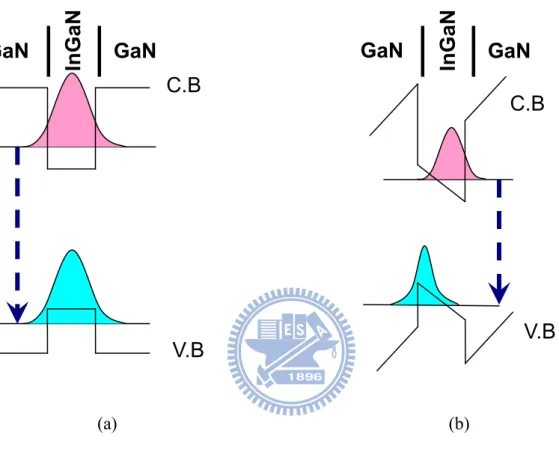
c-plane quantum well under QCSE is shown in Figs. 2.3.1(a) and (b). As can been seen, the well potential in the nonpolar nanostructure is not influenced by the built in polarization field and possess a higher wavefunction overlap and emission energy than polar nanostructure. Thus nonpolar is now a chance to improve the light emitting efficiency greatly and make a grand breakthrough in the III-V nitride system development.
2.4 Light polarization effect in nonpolar quantum wells
In addition to the advantage of no internal electric fields in growth direction, nonpolar orientation of the wurtzite crystal structures are also good for polarization-sensitive devices. In contrast to GaN films grown along the polar c-plane direction, do not exhibit any in-plane polarization anisotropy, m- and a-plane GaN films, where the c-axis lies in the film plane, exhibit significant polarization anisotropy in its light emission.
When GaN films are grown on c-plane substrates with similar hexagonal symmetry, there is no linear polarization emission happened under isotropic in-plane strain. However, a GaN film with an m-plane or a-plane orientation experience anisotropic in-plane strain resulted from the inherent lower symmetry of m and a plane. An in-plane polarization anisotropy has been observed in the PL spectra of
GaN/(Al,Ga)N MQWs [12, 21].
The coordinate system used for the investigation of the polarization properties is x//a[1120]、y//m[1100]、and z//c[0001], the three planes are perpendicular to each other. Take the m-plane GaN films for example, m-plane strain lifts the symmetry in the x-y plane of the wurtzite crystal and separates the original |X±iY>-like HH and LH states of unstrained WZ-GaN to |X>-like and |Y>-like states. A compressive strain along x induces a dilatation along y so that the energy of the |X>-like state is raised while the |Y>-like state is lowered. Valence bands are reconstituted to |X>-like, |Z>-like, and |Y>-like states in order of decreasing electron energy. Therefore, the valence band structure is altered that the lowest transition energy is totally linearly polarized in the x-direction (E⊥C), while the second lowest transition energy is totally linearly polarized in the z-direction (E//C). The third lowest transition energy which is linearly polarized in the y-direction will not show any PL intensity difference when we put the polarizer in x-z plane to get the polarization information.
The optical polarization anisotropy in GaN films with a nonpolar orientation can be used for polarization-sensitive photodetectors [22] and static as well as dynamic polarization filtering [23]. It has also been applied to achieve polarized emission in (In,Ga)N/GaN light-emitting diodes grown along nonpolar orientations [24].
(a) (b)
Fig. 2.3.1 A schematic energy band diagram of (a) nonpolar quantum well and (b) polar quantum well under QCSE.
C.B
V.B
In
GaN
GaN
GaN
C.B
V.B
In
GaN
GaN
GaN
Chapter 3 Metalorganic Chemical Vapor Deposition System
3.1 Introduction
For the past few years, metalorganic chemical vapor deposition (MOCVD) has become a commonly used technology for production of III-V compound semiconductor optoelectronic devices and electronic devices. The achievement of growing ultra-bright blue light emitting diodes by MOCVD makes this technology be a leading candidate for manufacturing optoelectronics devices. Briefly, MOCVD process relies on vapor transport of the group III alkyls combined with group V hydrides into heated substrate. At the heated substrate, the molecules pyrolyze to produce the group III and the group V elements needed for formation of the desired III-V semiconductors and subsequent reaction. Because these precursor molecules are so unstable at the growth temperature and the III-V solid is so stable, the thermodynamic driving force for MOCVD typically is enormous. MOCVD is sometimes described as a highly non-equilibrium process.
The first MOCVD system design for GaN growth was developed by Maruska and Tietjen. Soon after, Manasevit applied this technique to grow GaN onto sapphire substrates. The choice of sapphire substrate results from the facts that no bulk GaN substrates are available and a very stable material is required to deal with the high temperature required for GaN growth (around 1000 C). Metalorganic group III
sources are either liquids, such as trimethylgallium (TMGa), triethylgallium (TEGa), trimethylaluminum (TMAl) and triethylaluminum (TEAl), or solids such as trimethylindium (TMIn). For III-nitrides growth, ammonia (NH3) is most commonly
gaseous hydride source. Dopant materials can be metal organic precursors such as dimethylzinc (DMZn), cyclopenta-dienyl-maganesium (CP2Mg) and hydrides of
silence (SiH4) or disilance (Si2H6).
To optimize of MOCVD grown condition is typically done by empirical studies of external parameters such as growth temperature, V/III ratio, and mass flow rates. These studies have identified three regions of growth: mass transport limited, desorption and surface kinetically limited regimes. Conventional GaN MOCVD growth is usually performed in mass transport limited regime that takes place over a wide temperature (600~1100 C). Because the diffusion process is slightly temperature dependent, there exists a slight increase in growth rate in temperature range. In other words, in this temperature region growth is limited by mass transport of the column III reactant to the growing interface. Further research is needed in the understanding of the mechanism of III-nitrides growth by MOCVD.
3.2 MOCVD Reactor
There are several types MOCVD reactors which are designed for growing GaN. The most successful reactor is designed by Nakamura et al. The key issue for this
reactor is downward subflow of H2 and N2, which was claimed to improve the
interaction of the reactant gases with the substrate. The other important feature including separate the alkly inlet and ammonia to minimize predeposition reaction, the perpendicular subflow to suppresses thermal convections and rotating susceptor to enhance the film uniformity. To separate source flow is very important for nitride growth. Aluminum and ammonia would cause adduct in the gas phase. Magnesium and ammonia would prereaction in gas phase if alkly and hydride didn’t separate.
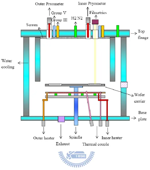
In this thesis, most experiments were done by EMCORE D180 or AIXTRON 2600G3 HT system. The EMCORE D180 MOCVD system is fully computer controlled, multiwafer-rotating-disk reactor system. The schematic reactor configuration shown in Fig. 3.2.1 is equipped with a double walled water-cooled stainless-steel chamber, a two-zone filament heater, and a loadlock chamber. The spindle rotation is by means of a high speed motor driving a toothed belt. A susceptor on top of the spindle provides support and restraint for the reference signals for controlling the heater temperatures. Temperature control is better than 1 C with the PID controlled ac low voltage power supplies. Openings are provided in the growth chamber for loadlock access and viewports, including pyrometer temperature measurements ports.
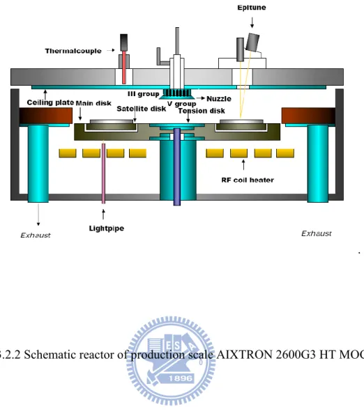
configurations. The schematic reactor configuration is shown in Fig. 3.2.2. It is equipped with a walled water-cooled stainless-steel chamber, and a RF coil heater. The rotation of the susceptor and satellite discs is by means of a low-speed motor driving a toothed belt and a N2 or H2 gas flow system, respectively. A suspector on
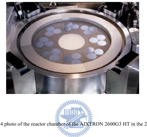
top of the supporting tube and the supporting disc provide support and restraint for the reference signals for controlling the heater temperatures. Temperature control is better than 1 C with the PID controlled dc low voltage power supplies. Opening is provided in the growth chamber, including pyrometer temperature measurement ports. Figure 3.2.3 shows a schematic of the susceptor of the AIXTRON 2600G3 HT in the 242 inch configurations. Figure 3.2.4 shows a corresponding photo of the reactor chamber. The gases enter the reactor chamber through the central inlet in the reactor lid (not visible in the photo) and stream radially outward across the deposition zone. The susceptor is heated by RF induction heating from below and rotates at rotation frequencies of typically 10 rpm. In addition the wafer discs are rotating utilizing AIXTRON’s patented Gas Foil Rotation technique. This double rotation insures highest uniformities.
3.3 In-Situ Reflectance Monitoring During III-Nitrides Growth
One of major limitations of III-nitrides technology was absence of homoepitaxial substrate. This limitation was usually overcome by growing a low-temperature (LT)
AlN or GaN nucleation layer on a sapphire substrate before the high-temperature (HT) growth. The LT nucleation layer serves as a template to increase nucleation site and improve the crystal quality of HT growth GaN layer. Although Wu et al. have reported the growth evolution of LT nucleation layer. Amano et al. and Akasaki et al. have also reported the process of GaN growth with AlN nucleation layer. Their studies were all restricted to ex-situ characterization with interrupted growth. In order to realize the growth information during growing GaN, we need an in-situ monitoring tool to extracting growth information.
The first report of in-situ monitoring during growing GaN was present by Nakamura et al. He investigated the infrared radiation transmission intensity (IR-RTI) oscillation for GaN growth with and without AlN nucleation layer. He concluded that thickness of AlN nucleation layer would strong effected the crystal quality of HT GaN film and verified the model proposed by Amano and Akasaki. This pyrometric interferometry has well developed in MBE for AlGaAs, GaAs, and InAs growths. However, there are several drawbacks such as infrared detection wavelength limitation, spectrum dispersion due to broad detection band, and the temperature drift during growth.
Recently, Breiland et al. develop a method that optical constants and growth rate can be simultaneously extracted from the in-situ normal incidence reflectance of a
growing thin film. Consider a general III-V compound bulk, we usually grow a thin film on a specific substrate. Suppose the thin film material is different from substrate, the reflectance and interference from the underlying interfaces is much difficult to present. Therefore, Breiland et al. develop a “virtual interface model” to revel the real reflectance in a multiple-layer system.
In this study, we use a spectral reflectivity system to measure the thickness and optical constants of “translucent” thin film layers on the substrates. Because of its wave-like properties, light reflected from the top and bottom surfaces of a thin-film layer can be in-phase so that reflections add, or out-of-phase so that reflections subtract. Whether the reflections in-phase or not depends on the wavelength of the light, as well as the properties of the epitaxial film.
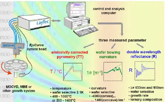
This system is PC-based and integrates measurement and analysis software with a spectrophotometer and fiber optic measurement hardware. Figure 3.3.1 shows the hardware configuration of EpiTune II for the planetary reactor. As mentioned above, this in-situ monitoring technique is a powerful tool for measuring the epitaxial growth rate. Apply this tool we can also do temperature calibrations and growth rate calibration for several different materials in a single run. In the former case, one can perform temperature calibrations with eutectic wafers (Al-coated Si wafers or Silver-coated Si waver) quickly and easily by plotting the reflectance as a function of
temperature, while the temperature of the reactor is ramped slowly. It is well known that the melting poing of aluminum and silver are 660 C and 961 C. As the temperature ramping up to the melting point, the reflectance would be drop down rapidly. Thus one could know the meter temperature is the metal melting point.
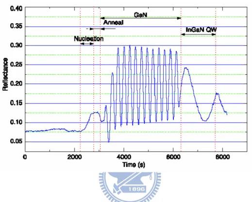
In the case of a material system with clearly different indices of refraction between an underlying layer and the layer to be probed, time-resolved Fabry-Perot like reflectance is utilized to determine the growth-rate and the crystalline quality of the growing wafers. There methods, EpiTune I and EpiTune II, can be applied in the case of nitride semiconductor structures where a step in refractive indices is present at the interface between the growing device structure and the sapphire wafer or in selected phosphorus and arsenic containing device structures. In addition, features in the traces at the beginning of the layer growth can be distinguished by the experienced process engineer, thus speeding up time to market for new processer and devices. Figure 3.3.2 exhibits such a trace for the case of an InGaN MQW structure as described above. The different steps like nucleation, anneal, buffer and MQW growth can be clearly distinguished. In addition to the sole measurement of the reflectivity as a function of time, EpiTune II offers the possibility to measure the emissivity corrected temperature for each wafer. A high repetition rate of the pyrometric temperature measurement and the probing of the reflectivity through the same optical
path facilitate an accurate determination of the emissivity corrected temperature, since pyrometry and reflectometry are practically performed on the same point on the wafer.
In conclusion, as devices become more complex and epitaxial wafer specifications more tighten, the MOCVD equipment for compound semiconductor manufacturing must also advance. The in-situ monitoring technique is simple and powerful, and gives the MOCVD users the really practical tool for looking at epitaxial growth while the growth is in progress.
.
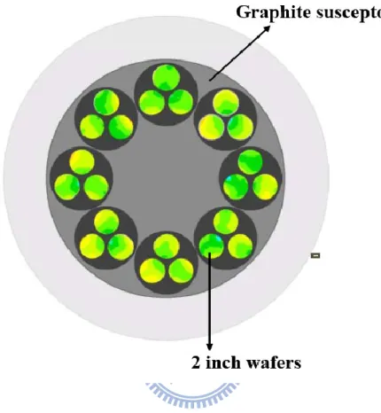
Fig. 3.2.2 Schematic reactor of production scale AIXTRON 2600G3 HT MOCVD system
Fig. 3.2.3 Layout of the AIXTRON 2600G3 HT susceptor in the 242 inch configuration.
Fig. 3.2.4 photo of the reactor chamber of the AIXTRON 2600G3 HT in the 242 inch configuration.
Chapter 4 Optical Properties of a-plane InGaN/GaN MQWs
4.1 Sample growth and fabrication
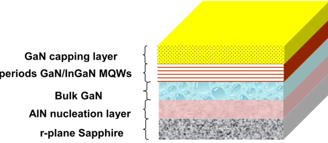
All epitaxial films were grown on r-plane sapphire in MOCVD reactor. Trimethylgallium, trimethylindium, and ammonia were the precursors used for sources of Ga, In and N in whole epitaxy process. At first, the r-plane sapphire substrate was treated by thermal annealing at 1090 ℃. Subsequently, a 30 nm thickness AlN nucleation layer was deposited at 600 ℃. The growth temperature was ramped up to 1120 ℃ to grow a-plane bulk GaN of 2 μm thickness. The MQWs structure was grown at 700 ℃ which consisted of 10 pairs of GaN barriers and InxGa1-xN wells. We controlled different growth time ranging from 1~3 minutes on
growing quantum well to get different active layer thickenss. Finally, the 50 nm capping layer of GaN was deposited. A schematic diagram of sample structure was shown in Fig. 4.1.1
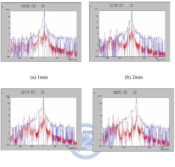
The ω-2θ scan measurements of high resolution x-ray diffraction (HRXRD) made with a Philips MRD X’pert PRO diffractometer using CuKα1 radiation were applied to quantify the quantum well and barrier thicknesses. The In composition could also be made sure. Fig. 4.1.2 is a schema of the (1120) a-plane orientation which defines the specific crystallographic index used in the HRXRD analysis. The dynamic diffraction simulation shown in Fig. 4.1.3(a)~(d) models the peak
locations of the HRXRD experimental results. The X-ray diffraction analysis confirmed that the In composition of the quantum well is around 23%, the GaN barrier is around 12 nm thick and the approximate well width for different growing time samples are 3, 6, 9, and 12 nm, respectively. We concluded the HRXRD measured result in Table 4.1.1.
Fig. 4.1.1 A schematic drawing of sample structure
Fig. 4.1.2 The specific crystallographic index used in the HRXRD analysis.
10 periods GaN/InGaN MQWs
r-plane Sapphire AlN nucleation layer
Bulk GaN GaN capping layer
(a) 1min (b) 2min
(c)2.5min (d)3min
Fig. 4.1.3 Experiment and simulation results of HRXRD ω-2θ scans for a-plane InGaN/GaN MQWs.
1min 2min 2.5min 3min
In composition 0.23 0.23 0.23 0.23
well
Table 4.1.1 The HRXRD measured layer thickness and composition
4.2 Photoluminescence properties
The optical characteristics of c-plane InGaN/GaN multiple quantum wells (MQWs) have been studied extensively [8, 9]. However, the optical properties of
a-plane InGaN/GaN MQWs are still worth investigating for assistance of fabrication
due to the lack of the internal field and possible different growth parameters. Since the interface roughness and treading dislocations in a-plane heterostructures are more complicated than those in c-plane heterostructures [20], the luminescence mechanism requires further clarification of the dependence of the optical characteristics on the different InGaN/GaN quantum well widths. Craven et al. had investigated optical characteristics of GaN/AlGaN MQWs with different well widths [7]; however, the issues related to well width dependence of a-plane InGaN/GaN MQWs have not been conferred yet. As mentioned in Section 2.2, localization effect plays an important role in polar c-plane InGaN-based structure luminescence. It is widely accepted that the high luminescence efficiency of polar InGaN-based structures is due to the exciton localization effect.
Photoluminescence spectroscopy is an un-contact, nondestructive method of examining the electronic structure and optical characteristics of materials. Photoluminescence is the emission of light from a material under optical excitation. It
needs an excited light source to induce the emission and the energy of the excited light source should be higher than the band gap energy of the material. Light is directed onto a sample where it is absorbed and electrons in the valence band would get the energy to jump into the conduction band then relatively produce a hole in the valence band. When an excited electron in the conduction band returns back to the valence band, it releases the energy which includes a radiative process and a nonradiative process.
The energy of the emitted light (photoluminescence) relates to the difference in energy levels between two states involved in the transition which are the excited state and the equilibrium state. The intensity of the emitted light is related to the contribution of the radiative process. The intensity and spectral content of a photoluminescence spectrum is a direct inspection of material properties.
The setup of our PL system is shown in Fig. 4.2.1. The pumping light source was a multi-mode and non-polarized Helium-Cadmium laser operated on 325nm with 20mW. After reflected by three mirrors, the laser light was focus by a lens which focal length was 5cm, to 0.1mm in diameter and the luminescence signal was collected by the same lens. The probed light was dispersed by 0.32 monochromator (Jobin-Yvon Triax-320) equipped with 1800, 1200, and 300 grooves/mm grating and which maximum width of the entrance slits was 1mm. The resolution was controlled
in 1nm by selecting 300 grooves/mm grating and slit of 0.1mm. We use long pass filter to avoid the laser coupling with the PL spectrum. Room temperature PL measurements were performed using the cw 325 nm He–Cd laser operating at an excitation level of 25 mW.
The CW PL spectra of these four samples measured at room temperature are shown in Fig. 4.2.2(a). The detailed MQW PL peak emission energy shown in Fig. 4.2.2(b) increases from 2.47eV to 2.79 eV with the decreasing well width could be fully attributed to the quantum size confinement effect. The similar peak energy of the samples of 9 and 12 nm is due to the weak quantum confinement effect in a larger well width. Figure 4.2.2(c) shows the PL peak emission intensity that gradually decreased with the increase of InGaN well width. When the well width is thicker than 6 nm, the PL intensity drops more quickly.The well width of optimal integrated PL intensity for a-plane would be thicker than relative thin polar quantum well [25]. In additional, the material quality, interface roughness and the excitonic Bohr radius would be considered in terms of the determination of optimal well width [7].
We then analyze different power dependences I ~Pα for the samples of different
well widths over a wide range of excitation power where I is the PL intensity, P is the pumping power intensity, and α is the power index. Power dependent PL measurement was carried out by using the CW 325 nm He–Cd laser which power
density was controlled from 2 to 200 mW/cm2.
In Fig.4.2.3, we show that the PL spectrum as a function of the excitation power for the samples with different well width. We obtained unshifted PL peaks with the increasing pumping power density, which is well known for a-plane hexagonal MQWs with the nonpolar characteristic and the flat band structure. [3] The stable spectral peak position under a wide range of excitation powers clearly indicates that the a-plane InGaN/GaN MQWs on the r-plane sapphire are nonpolar and thus free from the built-in electrostatic fields.
Fig.4.2.4 shows the PL integrated intensity among different excitation power density. Generally, I ~ P relation would satisfy with the condition when nonradiative channels saturate and radiative recombination predominates at elevated excitation. The power indices around 1 for our all samples indicate that the radiative recombination dominate in the optical transition [26] and is absolutely independent of InGaN well width, which also give the other evidence that no built-in electric field was observed within our a-plane InGaN/GaN MQWs with different well widths. However, such the a-plane MQWs without the built-in electric field within should not exhibit strong PL intensity dependence on the well width. [27] Other determining factors should account for the PL intensity drop with a thicker quantum well.
Fig. 4.2.1 The setup of PL system Mirror1 Mirror 2 Lens2 Filter 360nm Lens1 Triax320
25mW He-Cd laser (325nm)
InGaN MQWsFig. 4.2.2 (a) Room temperature PL spectra of a-plane InGaN/GaN MQWs with well width ranging from 3 to 12 nm.
Fig. 4.2.2(b)(c) Normalized PL energy peak and intensity plotted as a function of quantum well width.
2.0 2.2 2.4 2.6 2.8 3.0 3.2 3.4 3.6
PL Inten
sity
(arb. units)
Photon Energy (eV)
3nm 6nm 9nm 12nm 2 4 6 8 10 12 0.2 0.4 0.6 0.8 1.0 No rma li zed P L I n ten sit y (arb. u n its) Well Width (nm) 2 4 6 8 10 12 2.45 2.50 2.55 2.60 2.65 2.70 2.75 2.80 Em iss io n Pea k En e rg y (eV ) Well width (nm)
Fig. 4.2.3 PL spectrum as a function of the excitation power for a-plane InGaN/GaN MQWs with different well width.
2.0 2.2 2.4 2.6 2.8 3.0 3.2 3.4 3.6 3nm Norma li zed In tensity ( arb . u n it s)
Photon Energy (eV) 20mW 18mW 14mW 10mW 8mW 4mW 1mW 2.0 2.2 2.4 2.6 2.8 3.0 3.2 3.4 3.6 6nm 20mW 18mW 14mW 10mW 8mW 4mW 1mW No rm ali zed I n ten sit y (arb . u n it s)
Photo Energy (eV)
2.0 2.2 2.4 2.6 2.8 3.0 3.2 3.4 3.6 9nm No rm ali zed I n ten sit y (arb . u n it s)
Photon Energy (eV)
20mW 18mW 14mW 10mW 8mW 4mW 1mW 2.0 2.2 2.4 2.6 2.8 3.0 3.2 3.4 3.6 12nm No rm ali zed I n ten sit y (arb . u n it s)
Photon Energy (eV)
20mW 18mW 14mW 10mW 8mW 4mW 1mW
Fig. 4.2.4 The relation between PL intensity and excitation power density for a-plane InGaN/GaN MQWs with different well width.
1 10 100 0.01 0.1 1 3nm I~P1.05 PL Intensi ty (arb. units)
Excitation Power Density (W/cm2)
1 10 100 0.01 0.1 1 I~P1.06 6nm P L In ten sity (ar b. u nits )
Excitation Power Density (W/cm2)
1 10 100 0.01 0.1 1 PL Intensi ty (arb. units)
Excitation Power Density (W/cm2
) 9nm I~P1.04 1 10 100 0.01 0.1 1 I~P0.99 12nm PL Int en sit y (a rb. un its )
4.3 Temperature-dependent photoluminescence
In order to further understand whether the localization effect plays an important role in nonpolar InGaN MQWs as well as in polar c-plane InGaN nanostructure or not, PL spectra were measured under different temperature in the range of 20K to 300K using the CW 325 nm He–Cd laser.
Fig. 4.3.1 shows the evolution of PL spectra as a function of temperature for the a-plane InGaN/GaN MQWs with well width from 3nm to 12 nm. In these four samples, the decrease of PL intensity with increasing temperature is observed independent of quantum well width. Thermal quenching PL intensity with increasing temperature is a general phenomenon in III-V semiconductor nanostructure which is caused by carriers thermalization from the radiative recombination centers or/and localized states to the nonradiative recombination centers or/and delocalized states. [28] This thermal quenching behavior will be discussed later.
Moreover, at low temperature, there reveals three separated peaks in the PL spectrum, the most high energy peak located around 3.35eV in all samples is suggested to the signal of bulk GaN. The middle energy peak which is obvious in the samples of 3nm and 6nm well width but is merged with the lowest-energy side signal in the samples of 9nm and 12nm well width is supposed to the signal coming
from shallow localized states. [29] The lowest energy signal comes from the deep localized states. As can be seen, only the PL emission from excitons in deep localized states dominates the luminescence from 20K to room temperature, the other two higher energy emissions suffer an apparent quickly thermal quenching when the temperature increases. Along with the increase in temperature, the nonradiative energy relaxation of excitons occurs at shallow localized states, and then the efficient radiative recombination of excitons occurs mainly at deep localized states. The exciton dynamics at shallow delocalized states is very sensitive to the lattice temperature. When the temperature goes up, it is hard for excitons to stay stable in shallow localized states, the thermal dissociation of excitons occurs at shallow localized states, and electrons and holes are thermally excited into the delocalized states, thus, more transfer and relaxation processes happen which quench the emission from high energy states. [29]
Fig. 4.3.2 shows the Arrhenius plot of the normalized integrated PL intensity for the a-plane InGaN MQWs emission from deep localized states over the temperature range under investigation. The intensity reduction is remarkable, further compare these four figures, the degree of PL intensity reduction from 20K to 300K is more severe when the well width gets thicker which indicates a higher PL efficiency in the thinner well width samples. [30] We use the equation below to get a good fit to our
experimental data of the activation energy in thermally activated processes [31]:
I(T) = I0/[1+a*exp(-Ea/KBT)+b*exp(-Eb/KBT)]
where I(T) is the temperature dependent integrated PL intensity, I0 is the integrated
PL intensity at 20K, KB is the Boltzmann’s constant, a and b are the rate constants,
and Ea and Eb are activation energy for two different non-radiative channels. This
suggests that there are two non-radiative paths exist at the same time which one of them dominates in the low temperature region and the other dominate in the high temperature region. [32] The fitting result is listed in Table 4.3.1.
Since the activation energy we get from the four samples is much less than the bandgap energy difference between the well and the barrier, it is impossible to account the thermal quenching of InGaN MQWs emission for carriers thermalized from the InGaN wells to the GaN barriers. Therefore, the more reasonable explanation for the quenching of luminescence is that increasing temperature increases the probability of excitons to be trapped by nonradiative recombination centers within the well at the same time when carriers are activated out of the loacalization minima of potential fluctuation which may be caused by compositional、interface fluctuation and indium phase separation that always happened in InGaN quantum well layers [30].
samples, we further analyze the peak shift of InGaN MQW emission over the investigation temperature range. The result is shown in figure 4.3.3. In the samples with 3nm and 6nm well width, the emission energy decreases monotonically with increasing temperature. However, in the samples with 9 nm and 12 nm well width, the emission energy decreases at temperatures below 70K with uprising trend, then increases with increasing temperature from 70K to around 140K and finally decreases with further increase of temperature up to the room temperature. This red-blue-red shift of peak energy with increasing temperature is a characteristic of the exciton localization effect [30, 33]. From 20K to 70 K, it is considered that the observed dynamical redshift of the PL spectrum is caused by radiative excitons migrating into lower localized states. At elevated temperature from 70K to 140K, nonradiative recombination processes become more pronounced, some carriers recombination before reaching deeper band-tail states, resulting in a blueshift in the PL peak position. At higher temperature up to 300K, another redshift occurs mainly due to the temperature-dependent dilation of the lattice and electron–lattice interaction. [34, 35] Inhomogeneity due to interface fluctuation, InN/GaN segregation, and the band tail states originating from the high density of defects are responsible for the so-called S-shaped temperature dependent behavior in the samples with thicker well width. [31, 36]
Although the emission peak energy of samples with 3 and 6 nm well width do not show temperature induced S-curve, it is reasonable to infer that there may be still an exciton localization effect exists to a little extent for the two thinner samples. The total redshifts of the four samples over the temperature range under investigation are: 3 nm with 100 meV、6 nm with 75 meV、9 nm with 55 meV and 12 nm with 62 meV which indicates that the exciton localization effect may be much stronger in thicker well width. There is one point needed to be noted as compared with the well known shift of the band edge for nitrides of about 65meV without the exciton localization effect in polar structure, the total redshift of the emission peak energy in these four samples from 20K to 300K under the existing of localization effect showed rather big redshift variation with temperature. We couldn't give a clear explanation for such result now, a full understanding of the carrier dynamics in these nonpolar samples will probably emerge only after considerable further study. We can give two key points in this section : the first one is that in a-plane InGaN/GaN MQWs, samples with thicker well width of 9nm and 12nm reveals a more apparent localization effect which is most likely due to alloy、interface roughness fluctuations or worse crystalline quality in the MQWs. The second is that a deeper localization depth may exist in thinner 3nm and 6nm well width samples which could confine carrier tightly thus display an indistinctively visible S-shaped temperature dependent behavior.
Fig. 4.3.1 PL spectra as a function of temperature from 20K to 300K for a-plane InGaN/GaN MQWs with different well width.
360 380 400 420 440 460 480 500 520 540 Wavelength (nm) 20K 40K 60K 80K 100K 110K 120K 130K 140K 160K 180K 200K 220K 240K 260K 280K 300K 3nm P L In te ns ity (a .u .) 360 380 400 420 440 460 480 500 520 540 P L In te n si ty ( a. u .) Wavelength (nm) 6nm 20K 40K 60K 80K 100K 110K 120K 130K 140K 160K 180K 200K 220K 240K 260K 280K 300K 360 380 400 420 440 460 480 500 520 540 PL In te n sit y ( a.u.) 20K 40K 60K 80K 100K 110K 120K 130K 140K 160K 180K 200K 220K 240K 260K 280K 300K 12nm Wavelength (nm) 360 380 400 420 440 460 480 500 520 540 20K 40K 60K 80K 100K 110K 120K 130K 140K 160K 180K 200K 220K 240K 260K 280K 300K P L In te n si ty ( a. u .) Wavelength (nm) 9nm
Fig. 4.3.2 Normalized integrated PL intensity as a function of 1/T for the a-plane InGaN/GaN MQWs with different well width.
0.00 0.01 0.02 0.03 0.04 0.05 0.01 0.1 1 3nm Int eg rat ed PL Int en sit y (a.u. ) 1/T (1/K) 0.00 0.01 0.02 0.03 0.04 0.05 0.01 0.1 1 6nm In te g ra te d P L I n te n si ty ( a. u .) 1/T (1/K) 0.00 0.01 0.02 0.03 0.04 0.05 0.01 0.1 1 1/T (1/K) Inte g ra te d P L Inte n s it y ( a .u.) 9nm 0.00 0.01 0.02 0.03 0.04 0.05 0.01 0.1 1 1/T (1/K) Inte g ra te d P L Inte n s it y ( a .u.) 12nm
3nm 6nm 9nm 12nm
E1(meV) 46.5 9.7 22.4 33.4
E2(meV) 166.5 86.7 106.4 144.9
Table 4.3.1 The fitting result of activation energy for the a-plane InGaN/GaN MQWs with different well width.
Fig. 4.3.3 PL peak energy position as a function of temperature for a-plane InGaN/GaN MQWs with different well width.
0 50 100 150 200 250 300 2.76 2.77 2.78 2.79 2.80 2.81 2.82 2.83 2.84 2.85 2.86 2.87 2.88 3nm P ea k E n er g y (eV ) Temperature (K) 0 50 100 150 200 250 300 2.64 2.65 2.66 2.67 2.68 2.69 2.70 2.71 2.72 2.73 2.74 2.75 6nm Pe ak En ergy (e V) Temperature (K) 0 50 100 150 200 250 300 2.47 2.48 2.49 2.50 2.51 2.52 2.53 2.54 2.55 2.56 2.57 9nm Pe ak En er g y ( eV) Temperature (K) 0 60 120 180 240 300 2.43 2.44 2.45 2.46 2.47 2.48 2.49 2.50 2.51 2.52 2.53 12nm P ea k E n er g y (eV ) Temperature (K)
4.4 In-plane polarization effect
It was mentioned in section 2.4 that due to the inherent lower symmetry of non-polar heterostructure, a-plane InGaN/GaN MQWs is likely to experience anisotropic in-plane strain. A u-PL measurement was carried out at room temperature using the CW 325nm He-Cd laser and a visible polarizer was set in front of the light collection fiber to examine the polarization property of the four samples. In the case of the a-plane sample, an angle of 900 is defined to be parallel to the c [0001] axis (E║C) while the 00 is along m [1100] axis (E⊥C). The definition of crystal axes is shown in figure 4.4.1.
Figure 4.4.2 displays the polarization–dependent PL spectra of 3nm well width sample for polarization angles between 00 and 3600 in steps of 150. All results of polarization-dependent experiments were similar in these four samples.
The value of polarization degree ρ is defined as
ρ = (I⊥—I║)/ (I⊥+I║) , where I⊥ andI║ are PL intensities for E⊥C and E║C. Figure 4.4.3 shows the pretty symmetric of the normalized PL intensity versus the in-plane polarization angle. The polarization degree ρ of the four samples are 65.4%、66.8%、56.2%、and 58.3% for 3nm、6nm、9nm、and 12nm well width samples, respectively. No obvious difference
on polarization degree is observed with different well width. Figure 4.4.4 shows the PL spectra of the a-plane InGaN MQWs when the polarization of the emission is perpendicular and papallel to the c axis. According to the definition of crystal axes, the transition lowest in energy is allowed for E⊥C, and the transition under E║C must occur at the higher energy. There is an apparent 40~50meV blueshift of the E║C PL maximum with respect to the E⊥C one in 3nm and 6nm samples, but in the samples of 9nm and 12nm, no observable peak shift is found. We conclude the reason of this phenomenon to a large spectral broadening [37] resulted from a more apparent localization effect due to alloy、interface roughness fluctuations or worse crystalline quality in the thicker MQWs.
Fig. 4.4.1 The wurtzite GaN unit cell and the definition of crystal axes.
Fig. 4.4.2 μ -PL spectra of the a-plane InGaN/GaN MOWs for polarization angles between 00 and 3600 in steps of 150.
y (0
0,m-plane)
x (a-plane)
z (90
0,c-plane)
350 400 450 500 550 600 3nm In te n si ty ( arb. u n it s) Wavelength (nm) 00 150 300 450 600 750 900 1050 1200 1350 1500 1650 1800 1950 2100 2250 2400 2550 2700 2850 3000 3150 3300 3450 3600Fig. 4.4.3 Normalized μ -PL intensity versus the in-plane polarization angle for the a-plane InGaN/GaN MOWs with different well width.
0.2 0.4 0.6 0.8 1.0 0 30 60 90 120 150 180 210 240 270 300 330 0.2 0.4 0.6 0.8 1.0 3nm 0.2 0.4 0.6 0.8 1.0 0 30 60 90 120 150 180 210 240 270 300 330 0.2 0.4 0.6 0.8 1.0 6nm 0.2 0.4 0.6 0.8 1.0 0 30 60 90 120 150 180 210 240 270 300 330 0.2 0.4 0.6 0.8 1.0 9nm 0.2 0.4 0.6 0.8 1.0 0 30 60 90 120 150 180 210 240 270 300 330 0.2 0.4 0.6 0.8 1.0 12nm
Fig. 4.4.4 Normalized μ -PL spectra for E//c (900) and E⊥c (00) for the a-plane a-plane InGaN/GaN MOWs with different well width.
2.50 2.55 2.60 2.65 2.70 2.75 2.80 2.85 2.90 0.2 0.4 0.6 0.8 1.0 1.2 00 900 6nm No rma lize d P L In te n sity (a rb . u n its )
Photon Energy (ev)
2.69eV 2.74eV 2.60 2.65 2.70 2.75 2.80 2.85 2.90 2.95 3.00 0.2 0.4 0.6 0.8 1.0 1.2 00 900 3nm N orm ali ze d P L I nt en sity (arb . u nits)
Photon Energy (eV)
2.81eV 2.85eV 2.35 2.40 2.45 2.50 2.55 2.60 2.65 2.70 2.75 0.2 0.4 0.6 0.8 1.0 1.2 00 900 9nm No rma lize d P L In te n sity (a rb . u n its )
Photon Energy (ev)
2.35 2.40 2.45 2.50 2.55 2.60 2.65 2.70 2.75 0.2 0.4 0.6 0.8 1.0 1.2 00 900 12nm N or m ali ze d PL Int ensi ty (arb. un its)
4.5 Summary
In conclusion, ten pairs of a-plane InGaN/GaN MQWs of well width ranging from 3 to 12 nm grown by MOCVD on r-plane sapphire were investigated. No built-in electric field was observed in the power dependent PL measurement for all samples. However, the PL emission intensity decreases as the quantum well width increased. Moreover, the localization effect of a-plane MQWs was investigated by temperature dependent PL experiment. The experiment reveals that a more apparent localization effect existed in a thicker well width which is most likely due to alloy、 interface roughness fluctuations or worse crystalline quality in the MQWs. Finally, in-plane polarization effect of a-plane InGaN/GaN multiple quantum wells emission was investigated. An average degree of linear polarization about 60% is got in these four a-plane InGaN/GaN MQWs.
Chapter 5 Characteristics of a-plane InGaN/GaN Green LEDs
5.1 Introduction
Recently, nitride-based LEDs have been attracting great attention due to the potential in solid-state lighting. However, the conventional c-plane nitride-based QWs suffer the QCSE, due to the existence of spontaneous and piezoelectric polarization fields parallel to [0001] c-direction. It results in spatial separation of electron and hole wave functions in the QWs, which reduces carrier recombination efficiency and causes red-shifted emission. For example, 450-nm blue LEDs can achieve an external quantum efficiency (EQE) of 30%~40%, while records for 520-nm green LEDs merely reach 20% [38]. This is because the higher InN fraction incorporated in MQWs results in larger QCSE and more serious InN separation. Therefore, eliminating QCSE is one of the essential methods to increase quantum efficiency especially in green InGaN/GaN LEDs. To avoid such polarization effects, several methods of epitaxial growth of the QWs along crystal-lographic directions without polarization have been proposed, such as m axis and a axis GaN growth using different substrates. Unlike traditional c-plane growth, polarization discontinuities do not occur at the heterointerfaces along either the m- or the a-axis.
Hence, internal electric fields are absent in nonpolar QWs resulting in a flat-band condition. In addition, the nonpolar GaN films exhibit optically polarized spontaneous