This work was supported by the National Science Council of Taiwan under Grant NSC94-2215-E-009-044.
I
NTRODUCTION
To provide digital video services on handheld terminals in a mobile environment, the terminal devices must be customized for better mobility and battery-life usage. Nowadays, several orthog-onal frequency-division multiplexing (OFDM)-based standards are designed for such applications and will share this market. These standards are terrestrial digital multimedia broadcasting (T-DMB), integrated services digi-tal broadcasting-terrestrial (ISDB-T), digidigi-tal video broadcast-handheld (DVB-H), and medi-aFLO. The T-DMB is based on a digital audio broadcasting (DAB) system and improves the error correction part of a DAB system. The ISDB-T is a band-segmented transmission (BST) OFDM-based system that consists of a set of common basic frequency blocks. The mediaFLO and DVB-H use the coded orthogonal frequency division multiplexing (COFDM) modulation method. Some comparisons and survey work were recently reported in [1]. The DVB-H [2] system, enhanced from the digital video broad-casting-terrestrial (DVB-T) [3] broadcasting sys-tem, is proposed for such environments. In addition, because of provided data rates in DVB-H services and the small-size displays of typical handheld devices, video coding methods, such as H.264/AVC (advanced video coding) and other high-efficiency video-coding standards are pro-posed [4].
In this article, we present a design case of DVB-T/H baseband receiver design. We focus on algorithm development, architecture design, and system-level integration for the receiver. In addition to meeting system performance require-ments, we also consider reducing power con-sumption at different design phases. In the initial phase, we construct a MATLAB [5] simulation-based platform, where we can concentrate on algorithm development, to meet performance requirements under different specified channel environments. Each algorithm/functional module is verified by the proposed platform via perfor-mance evaluation. In the architecture design phase, we check both data flow and computa-tional loads among all funccomputa-tional modules to achieve a cost-effective solution. For system-level integration, several silicon IP for both inner and outer receiver parts are developed and inte-grated in 0.18 µm complementary metal-oxide semiconductor (CMOS) process. This test chip occupies 6.9 × 5.8 mm2and consumes 250 mW
at the highest data rate specified in a DVB-T/H system.
The rest of this article is organized as follows. First, an overview of the DVB-T/H baseband processing is given, where the major differences between DVB-T and DVB-H are highlighted. Then, we introduce our design flow including algorithm development, architecture design, and system-level integration. Several memory-effi-cient methods and low-power techniques are described and discussed. Then a test chip with measurement results is presented.
O
VERVIEW OF
DVB-T/H B
ASEBAND
S
YSTEM
A block diagram of the DVB-T transmitter is shown in Fig. 1a [3]. The input transport stream is mainly from MPEG-2 artworks. There are two steps in the channel coding: one is the outer coder, a Reed-Solomon (RS 204,188) coder; the other is a punctured convolutional coder. In addition, the corresponding interleaving meth-ods (i.e., outer and inner interleaver) are adopt-ed. If required, the inner interleaver can integrate two channel-coded streams into a sin-gle slot when the transmitter is working in hier-archical mode. The mapper module is using three constellation schemes: quadraturephase-A
BSTRACT
Mobile video services have generated a lot of interest recently. To reach a cost-effective solu-tion, design trade-offs among system performance, hardware complexity, and power consumption must be considered in the early design phase of such applications. In this article, we present a sys-tem overview, simulation platform, and hardware design of a DVB-T/H baseband receiver. Starting with a design platform, several algorithms on both inner and outer receivers are developed to meet target system performance under different chan-nels. Then, system architecture and related key modules are explored, taking into account both sil-icon area and power consumption. Finally, several design issues related to the integration of the pro-posed DVB-T/H inner and outer receivers are addressed.
T
OPICS IN
C
IRCUITS FOR
C
OMMUNICATIONS
Lei-Fone Chen and Chen-Yi Lee, National Chiao Tung University
Design of a DVB-T/H COFDM Receiver for
Portable Video Applications
■Figure 1. Block diagram of DVB-T/H system: a) DVB-T baseband transmitter; b) DVB-H system. MPEG2 TV SERVICE MPEG2 TV SERVICE MPEG2 TV SERVICE Inner interleaver Guard interval insertion
Mapper adaptationFrame
Receiver New to DVB-H Channel 2K 4K 8K DVB-H TPS DVB-T modulator 2K 4K 8K DVB-H TPS DVB-T modulator Mux TS TS MPE-FEC MPE IP IP DVB-H IP encapsulator Time slicing Transmitter MPEG2 TV SERVICE Mux adaptation, energy dispersal Outer code FEC blocks OFDM modulation DVB-T baseband transmitter Inner code Outer interleaver Pilot and TPS signals OFDM To aerial
MPEG-2 source coding and multiplexing Splitter Transport mux Program mux Video coder Audio coder Data coder D/A (a) (b) RF front-end MPE-FEC MPE DVB-H IP decapsulator Time slicing Mux adaptation, energy dispersal Outer code Inner code Outer interleaver
modulation (QAM), and 64 QAM to transform bit information into complex data. Before the follow-up OFDM modulation, the transmission parameter signal (TPS) is inserted into the DVB frequency-domain frame structure. Meanwhile, both scattered and continual pilots are included for synchronization and channel estimation on the receiver side. The OFDM module conducts an inverse fast fourier transform (IFFT) opera-tion to convert 8K or 2K mode symbols into time-domain symbols. In the last step, cyclic pre-fix of the time-domain symbols are inserted to prevent multipath interference before passing to the radio frequency (RF) front-end module. All basic modules of DVB-T baseband receiver are inverse operations of transmitter blocks.
Figure 1b shows an overview of a DVB-H baseband processing system [2] derived from the existing T standard. The payload of DVB-H includes IP datagrams or other network layer datagrams encapsulated into multiprotocol encapsulation (MPE) sections [6] and then passed to an MPEG-2 multiplexer that is shared by other MPEG-2 TV services.
The major differences between DVB-T and DVB-H baseband processing are the following: 4K OFDM mode, in-depth interleaver, updated TPS code, and additional 5-MHz channel band-width. In the data link layer, an additional multi-protocol encapsulation-forward error correction (MPE-FEC) [6] frame structure is used. In addi-tion, the suspend mode of baseband processing must be developed for the time-slicing opera-tion. These new features are added to improve system performance and to reduce the average power consumption in DVB-H mode. Note that the new 4K mode OFDM is adopted for trading off mobility and single-frequency network (SFN) cell size, enabling single-antenna reception at high speeds. The time-slicing operation is a method to transport lower bandwidth require-ment data in usable higher-provided bandwidth, and it could suspend the RF and baseband mod-ules to reduce power consumption. The in-depth interleaver uses an existing 8K mode interleaving method to perform the interleaving operation in 4K/2K OFDM symbols to reduce probability of burst errors [7, 8]. A more in-depth discussion on system behavior and performance analysis of the DVB-H system can be found in [9]. Note that performance improvement of the MPE-FEC and power saving via the time-slicing oper-ation mode are the main research topics of interest for the DVB-H system.
DVB-T/H B
ASEBAND
R
ECEIVER
D
ESIGN
Our receiver design schedule includes two phas-es: algorithm development and integrated circuit (IC) implementation. For the former, we use the MATLAB simulation-based platform to develop various algorithms to meet system specifications. The main task in this domain is focusing on algorithm development and fixed-point word-length analysis. When several algorithms are developed to meet system specifications, all functional modules must transfer to fixed-point
each internal signal with minimum performance loss. After signal word-lengths are confirmed, these fixed-point simulation results are reserved and prepared for test bench coding in the fol-low-up IC implementation phase.
Basically, cell-based CMOS IC design flow is adopted in the second phase. In the hardware description language (HDL) coding step, if the synthesized HDL codes cannot meet power, speed, and area requirements, we go back to the first phase to refine the system algorithms and architectures. Meanwhile, the refined algorithms must meet the performance requirement for sys-tem specifications.
All modules in IC implementation are checked by specified testbenches from the algo-rithm development phase. This procedure can guarantee that the behavior of all modules in IC implementation corresponds to the functional blocks defined in the algorithm development phase.
For algorithm design, we build a simulation platform to observe overall system behavior and evaluate performance results of our proposed schemes under different channel conditions. For the architecture design, we double check the I/O behavior of each module and analyze data flow among different modules so that redundant operations can be removed without degrading the overall system performance. In addition, spe-cific memory organization and data reuse schemes are developed to reduce memory accesses. Finally, we propose power-saving schemes in computation-intensive modules to reduce power consumption, such as in a fast fourier transform (FFT) processor, Viterbi decoder, and outer interleaver.
S
IMULATIONP
LATFORMD
ESIGNOur proposed simulation platform includes a transmitter, channel models, and a receiver as shown in Fig. 2a. The transmitter includes chan-nel coding and OFDM modulation as defined in the standard. The channel coding includes the scrambler, RS encoder (outer coder), outer interleaver, punctured convolutional encoder (inner coder), and inner interleaver. A QAM modulator supporting QPSK, 16 QAM, and 64 QAM is applied to the OFDM modulation. Both TPS coding and pilot insertion are performed before the IFFT operation. The IFFT operation must support three modes of IFFT: 8K and 2K mode operations for the DVB-T system and a 4K mode operation for the DVB-H system.
For channel models, the multipath profiles are developed based on [4]. In addition, the fol-lowing effects are taken into account: Doppler effect, carrier frequency offset (CFO) effect, sampling clock offset (SCO), and additional white gaussian noise (AWGN).
The receiver covers both inner and outer modules, where the former targets synchroniza-tion and OFDM demodulasynchroniza-tion, and the latter performs channel decoding operations. The inner receiver includes timing synchronization, frequency synchronization, the FFT operation, channel equalization, and TPS decoding. The inter-symbol interference (ISI) effect will destroy the orthogonality of OFDM symbols and hence Basically, cell-based
CMOS IC design flow is adopted in the second phase.
In the hardware description language
(HDL) coding step, if the synthesized HDL
codes cannot meet power, speed, and area requirements, we go back to the first phase to refine
the system algorithms and
must be minimized. Here, we propose a three-stage timing synchronization scheme to identify symbol location to avoid ISI and reduce the tim-ing offset of received signals as well. In the first stage, the timing synchronizer uses the normal-ized maximum correlation method to detect the operation mode (2K, 4K, or 8K) and guard inter-val ratio (1/32, 1/16, 1/8, or 1/4) of the received signal. Meanwhile, the synchronizer locates the coarse symbol boundary. The second stage (fine symbol synchronization) and the third stage (timing tracking) are operated separately in the
frequency domain. The fine symbol synchroniza-tion exploits the linear phase rotasynchroniza-tion of scat-tered pilots in each OFDM symbol to estimate symbol timing offset. Then the symbol boundary is updated. In the third stage, we calculate the phase drift of continual pilots in the same sub-carrier location between continuous OFDM symbols, because this phase drift is caused by sampling clock offset. To reduce sampling clock offset, the phase drift information is passed to the interpolator at the input of baseband receiv-er to resample receiving signal.
■Figure 2. The proposed DVB-T/H baseband simulation platform: a) system data flow; b) performance results (left) and comparison (right).
Performance comparison about Doppler effect
Proposed design DIB7700-P[14]DiBCom DIB7000-H[14]DiBCom
70 Hz @ 2K mode*1
20 Hz @ 8K mode*1 10 Hz @ 2K mode*2 130 Hz @ 8K mode *3
Doppler tolerance
*1: *2: *3:
64QAM, GI = 1/8, code rate = 2/3, Rayleigh channel with Doppler effect
64QAM, GI = 1/32, code rate = 2/3, TU6 mode 16QAM, GI = 1/4, code rate = 1/2, TU6 mode System
condition Scrambler Outercoder interleaverOuter coderInner interleaverInner
TPS and pilot insertion QAM
modulation OFDM(IFFT) insertionGI
Ricean/Rayleigh multipath Doppler effect CFO Clock offset FFT
window FFT detectionSP mode estimationChannel Equalizer TPS decode andpilot remove
QAM demodulation De-inner interleaver De-inner coder De-outer interleaver De-scrambler De-outercoder
(a) (b) Transport stream Fine symbol synchronization Sampling frequency tracking AWGN
ADC Interpolator/decimation Carrier frequencycompensator GI/modedecision synchronizationCoarse symbol Pre-FFTAFC Transport
stream
Post-FFT AFC Carrier frequencytracking
SNR
Overall performance @ Rayleigh channel + Doppler 70 Hz 2K mode, GI = 1/8, code rate = 2/3, SCO = 20 ppm, CFO = 20 ppm
15 10 10–4 BE R 10–5 10–6 10–3 10–2 10–1 20 25 30 35 QPSK 16-QAM 64-QAM Perfect sync Ideal
In OFDM systems, the carrier frequency offset (CFO) effect will contaminate the signal in each sub-carrier and cause inter-carrier interference (ICI). To reduce ICI and over-come the Doppler frequency drift, a three-stage frequency synchronization scheme is developed to estimate the fractional part of the CFO in time-domain and the integer part of the CFO in the frequency-domain. Then, a CFO tracking scheme is used to reduce the residual CFO. The first stage is to estimate the phase rotation between the guard interval and the copied data in the OFDM symbol for the fractional part of the CFO. The integer part of CFO is estimated in the frequency-domain by a guard band detection method in the second stage. In the third stage, we apply a joint SCO/CFO tracking scheme to estimate the residual CFO and Doppler frequency drift. Outputs from these three-stage estimation/tracking schemes are then exploited to compensate the CFO effects.
To support variant-length FFT operation, a radix-8 hierarchical memory-based FFT proces-sor [10] is exploited to realize 2K/4K/8K FFT operations. In the channel equalizer design, we apply two 1D linear interpolators for channel estimation and zero-forcing method for channel equalization. Note the TPS code contains the information required for demodulation and channel decoding, such as guard interval ratio, transmission mode, QAM method, hierarchical information, and the code rate of the punctured convolutional code. This TPS decoder uses a voting scheme to decide the final answer from a TPS information set in TPS carriers. A 64-level
soft-decision QAM demodulation is used to improve the system performance gain.
A path-merging and path-prediction Viterbi decoder [11] is adopted in the outer receiver. It can adjust the traceback length and memory accessing times based on the results from the inner receiver. For the outer de-interleaver, we design a 2D address generator unit that can per-form the de-interleaving operation in a single one-port memory. The RS decoder applies the decomposed key equation solver to achieve bet-ter area efficiency [12].
To overcome the Doppler effect in a mobile environment, a robust channel equalizer with CFO tracking is required. From mathematical analysis, the Doppler effect can be modeled as a dynamic CFO drift in each sub-carrier of the OFDM symbol. The Doppler tolerant range of the proposed design is limited by channel equal-ization and CFO tracking schemes. Here we adopt two 1-D linear interpolators for channel estimation and a joint SCO/CFO tracking scheme for frequency synchronization to over-come this frequency drift issue. Our proposed system can tolerate a Doppler effect of 70 Hz in 2K mode and 20 Hz in 8K mode under the fol-lowing conditions: Rayleigh multipath with a sig-nal-to-noise ratio (SNR) loss of less than 2 dB.
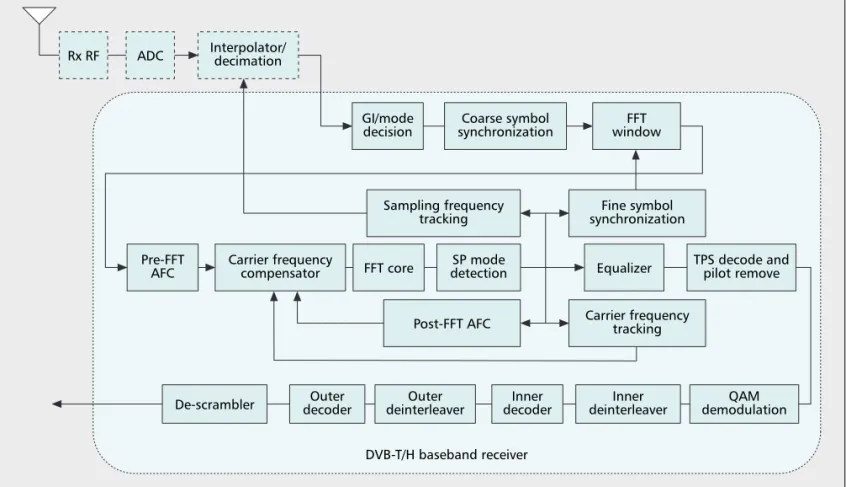
Figure 2b shows an example of the floating-point performance results under the following conditions: 2K mode, GI=1/8, coding rate=2/3, SCO=20 ppm, CFO=20 ppm, Rayleigh multi-path channel with a Doppler effect of 70 Hz. Also, a brief comparison of our proposal with other solutions in terms of the Doppler toler-ance range is shown in the left-hand side of Fig. ■Figure 3. The proposed DVB-T/H baseband receiver.
DVB-T/H baseband receiver Rx RF ADC Interpolator/decimation
GI/mode decision Coarse symbol synchronization Sampling frequency tracking Fine symbol synchronization
Post-FFT AFC Carrier frequencytracking FFT window
Pre-FFT AFC
De-scrambler decoderOuter deinterleaverOuter decoderInner deinterleaverInner demodulationQAM Carrier frequency compensator FFT core SP mode detection Equalizer TPS decode and pilot remove
2b. Note that different channel conditions and transmission parameters may result in different Doppler performance results.
A
RCHITECTURED
ESIGNA block diagram of the proposed DVB-T/H baseband receiver is shown in Fig. 3. The pro-posed design is compro-posed of synchronization units, a 8K/4K/2K FFT processor, a 2-D channel equalizer, a TPS decoder, an inner de-inter-leaver, a Viterbi decoder, an outer interde-inter-leaver, and an RS (204, 188) decoder.
Inner Receiver Design — The structure of the inner receiver is shown in Fig. 4a. When data arrives, the timing synchronization system detects key parameters for the OFDM frame structure, including operation mode (8K/4K/2K) and guard interval ratio (1/4, 1/8, 1/16, 1/32). After detect-ing the operation mode and guard interval ratio, the coarse symbol boundary is determined by the normalized maximum correlator. In the mean-time, the fractional part of the CFO is estimated based on the phase rotation between guard interval data and partial symbol data. The FFT
■Figure 4. Proposed hardware architecture for the DVB-T/H baseband receiver: a) receiver structure; b) sequential power management.
Chein search 64 ACS 64 ACS 64 ACS Demapper Channel estimator Freq. sync. FFT core SP order detection Module 2 Module 1 Module 3 Channel equalizer Channel estimator FFT processor Synchronizers Power management TPS decoding Channel decoder Transport
stream demappingQAM
(a) (b) Outer receiver 64 ACS 64-path metric Branch metric Survivor memory Syndrome calculator Key equation solver Error value evaluator Descrambler Transport stream Error corrector Universal outer deinterleaver memory Outer deinterleaver address generator Inner receiver Symbol memory Queuing memory Queuing memory Queuing memory Symbol memory Bitwise memory 36 6 24 TPS decoder Bitwise deinterleaver Time sync. Data input 8 9 FFT memorymemoryFFT Symbol deinterleaver ADC Tuner Channel equalizer
complete OFDM symbol is received. The FFT core is based on a radix-8 butterfly unit with a 64-word pre-fetch buffer and dynamic scaling method to reduce word length [10].
The scatter pilot (SP) order detection and post-FFT CFO estimation is activated right after the FFT symbol is processed. These two functions require three OFDM symbols to detect the SP order and to compute the integral part of the CFO that is used to compensate FFT input data to reduce ICI effect. After detecting SP order, the channel estimator extracts SP information from the OFDM sym-bol. To obtain correct channel frequency response (CFR), the channel estimator requires four OFDM symbols to obtain 2D CFR infor-mation. Using two half-size queuing memory and retiming access schemes, only three symbol-size memory blocks are required for stored data. After the channel estimator collects sufficient CFR information, the channel equalizer equal-izes data that will be sent to the symbol de-interleaver memory.
After the channel equalizer starts outputting data, we must decode the TPS containing opera-tion mode, QAM modulaopera-tion method, guard interval ratio, symbol interleaving order, and coding rate of the inner decoder. Without the decoded TPS information, the inner de-inter-leaver, QAM receiver, and outer receiver cannot be activated. The complete TPS information is embedded in one OFDM frame (68 OFDM sym-bols) of the DVB-T/H frame structure, implying at least one OFDM frame is required to collect complete TPS codes.
In the final stage of this inner receiver, two operations must be performed: QAM demodula-tion and inner de-interleaving. We exchange the symbol de-interleaving operation order before the QAM demodulation to reduce memory over-head when the word-length of the soft-decision QAM demodulation is longer than that of the channel equalization output. Based on this reordering scheme, the required word length of the symbol de-interleaving memory is reduced from 36-bit to 24-bit, saving about 145 K-bit memory space.
For each bit-wise interleaving section, the symbol de-interleaver outputs 126 de-interleaved data to a 64-level soft decision QAM receiver. The QAM receiver outputs the demodulated data that are stored into bit-wise de-interleaving memory. After 126 demodulated data are filled into bit-wise interleaving memory, both the sym-bol de-interleaver and the QAM receiver will hold until the bit-wise de-interleaver transfers one complete section data.
Outer Receiver Design — The structure of the outer receiver is also shown in Fig. 4a. The Viterbi decoder receives bit-wise de-interleaver data to decode punctured convolutional code. The outer de-interleaver can be realized by the general memory structure with a specific address generator. The required memory space can be reduced depending on the RS (204,188) decod-ing length. There are five steps in the RS (204,188) decoder: namely, syndrome calculator, key equation solver, chien search, error value
the RS decoder, the descrambler decodes the scrambled data stream except for the synchro-nization words.
S
YSTEML
EVELP
OWERM
ANAGEMENTU
NITThe tasks allocated in this receiver design can be divided into three working phases: namely, the initialization phase, equalization phase, and channel decoding phase. We develop a multi-stage power management (PM) in the proposed receiver to schedule these tasks working in dif-ferent phases to reduce power consumption and minimize signal transition activities. Figure 4b shows the sequential power management for this test chip.
In the initial phase, only two synchronization units and the FFT processor must be activated for timing and CFO estimation. Hence, the PM turns off the clock trees and holds the signal transition from channel equalizer to descram-bler. After the acquisition of the timing and CFO estimation, the receiver enters the equal-ization phase, where the PM turns on both the channel equalizer and the TPS decoder to get the TPS code in one DVB-T/H frame. Once the TPS decoding is correct, the PM starts to turn on the clock tree of the outer receiver and allows only signal transition in data compensation, demodulation, and decoding. Hence, signal switching activities are further reduced to save more power consumption.
Figure 5b shows the summary of power sav-ing schemes we used. These schemes are adopt-ed in algorithm, architecture, and system-level implementation. They can be classified into three types:
• Memory access time reduction • Word-length reduction • Redundant power elimination
In the FFT module, the hierarchical memory structure can reduce memory access time, and the dynamic scaling approach can keep the data accuracy without increasing extra word-length. The soft-decision de-QAM reordering can avoid increasing word-length in the symbol de-inter-leaver. The path-merging and path-prediction schemes can reduce the access time of survival memory of Viterbi decoder. The single memory structure with the specific address generation unit (AGU) in the outer de-interleaver can reduce the number of memory banks. Finally, the PM unit eliminates the redundant power consumption of this receiver processor in both initialization and equalization phases.
I
MPLEMENTATION
R
ESULTS
A DVB-T/H COFDM baseband test chip [12] using the aforementioned techniques was designed and fabricated in a 0.18 µm single-poly six-metal CMOS process with an area of 6.9 × 5.8 mm2. The logic gate count is about 371 K,and the overall embedded memory size is about 158 kilobytes. Figure 5a shows the microphoto of this test chip containing both inner and outer receivers. The largest module and main power consumer of the test chip is the FFT processor, with dual-bank embedded memory, occupies about 40 percent of the total area and consumes In the initial phase,
only two synchronization units and the FFT processor must be activated for timing and CFO estimation. Hence, the PM turns off the clock trees and holds the signal
transition from channel equalizer
44 percent of total power consumption. The overall power consumption is about 250 MW at the highest data rate (31.67 Mb/s) of DVB-T/H system specifications.
C
ONCLUSION
In this article, we present a single-chip COFDM-baseband receiver based on DVB-T/H specifica-tions. Several techniques covering algorithm design and architecture exploration to reach a cost-effective solution were reported. Specifical-ly, reducing storage space and minimizing switch-ing activities are explored to reach a better power consumption index. A test chip demon-strates that a low-power and highly-integrated DVB-T/H baseband receiver can be effectively realized in a 0.18 µm CMOS process for portable video applications.
A
CKNOWLEDGMENTThe authors would like to thank their col-leagues within the SI2 research group of National Chiao Tung University for many fruit-ful discussions and for support in this DVB-T/H project. They also thank the Chip Implementation Center (CIC) for testing and measurement services.
R
EFERENCE[1] Y. Wu et al., “Comparison of Terrestrial DTV Transmis-sion Systems: ATSC, DVB-T and ISDB-T,” IEEE Trans. Broadcasting, June 2000.
[2] ETSI EN 302 304 V1.1.1, “Digital Video Broadcasting (DVB): Transmission System for Handheld Terminals (DVB-H),” Nov. 2004.
[3] ETSI EN 300 744 V1.5.1, “Digital Video Broadcasting (DVB): Framing Structure, Channel Coding and Modula-tion for Digital Terrestrial Television,” Nov. 2004. [4] ITU-T Rec. H.264/ISO/IEC 14496-10 AVC draft/final draft,
“Joint Video Specification,” May 2003.
■Figure 5. a) Chip microphoto; b) power saving schemes in the test chip.
FFT operation Hierarchical memory structure Dynamic scaling
Lower memory access power Wordlength reduction (a)
(b)
Used schemes Effects
Reordering De-QAM Reordering operations Storage space reduction Viterbi decoder Path merging, path prediction Less memory access power Outer de-interleaver Single memory structure with
specified address generator
Less memory access power Power management Multiple operation phases Redundant power elimination
In the FFT module, the hierarchical memory structure can reduce memory access time, and the dynamic scaling approach can keep
the data accuracy without increasing extra word-length. The soft-decision de-QAM reordering can avoid increasing word-length in
the symbol de-interleaver.
Computing, http://www.mathworks.com/
[6] ETSI EN 301 192 V1.4.1, “Digital Video Broadcasting (DVB): DVB Specification for Data Broadcasting,” Nov. 2004. [7] H. Joki, J. Paavola, and V. Ipatov, “Analysis of
Reed-Solomon Coding Combined with Cyclic Redundancy Check in DVB-H Link Layer,” 2nd Int’l. Symp. Wireless Commun. Sys., Siena, Italy, Sept. 2005.
[8] H. Joki and J. Paavola, “A Novel Algorithm for Decapsu-lation and Decoding of DVB-H Link Layer Forward Error Correction,” IEEE ICC, Istanbul, Turkey, June 2006. [9] G. Faria et al., “DVB-H: Digital Broadcast Services to
Hand-held Devices,” Proc. IEEE, vol. 94, no. 1, Jan. 2006. [10] Y.W. Lin, H.Y. Liu, and C.Y. Lee, “A Dynamic Scaling
FFT Processor for DVB-T Applications,” IEEE JSSC, vol. 39, no. 11, Nov. 2004, pp. 2005–13.
[11] C. C. Lin et al., “Design of a Power-Reduction Viterbi Decoder for WLAN Applications,” IEEE Trans. Circuits and Sys., vol. 52, no. 6, June 2005, pp. 1148–56. [12] H. C. Chang, C. B. Shung, and C. Y. Lee, “A Reed-Solomon
Product-Code (RS-PC) Decoder Chip for DVD Applications,” IEEE JSSC, vol. 1, no. 2, Feb. 2001, pp. 229–36.
[13] L.F. Chen et al., “A 1.8V 250mW COFDM Baseband Receiver for DVB-T/H Applications,” ISSCC Dig. Tech. Papers, Feb. 2006, pp. 262–63.
A
DDITIONALR
EADING[1] DiBcom, DIB7700-P, DIB7000-H DVB-H/T receiver chip, data sheet, 2005.
LEI-FONECHEN(lfchen@si2lab.org) received his B.S. and M.S. degrees in computer science and information engineering from Chung-Hua University, Taiwan in 1998 and 2000, respectively. He is currently working toward a Ph.D. degree in the Department of Electronics Engineering, National Chiao Tung University, Hsinchu, Taiwan. His research inter-ests include digital signal processing and wireless commu-nications, VLSI for baseband transceivers, and low-power architecture.
CHEN-YILEE[M’01] (cylee@si2lab.org) received his B.S. degree from National Chiao Tung University in 1982, and his M.S. and Ph.D. degrees from Katholieke University Leu-ven, Belgium in 1986 and 1990, respectively, all in electri-cal engineering. In February 1991 he joined the faculty of the Electronics Engineering Department, National Chiao Tung University, where he is currently a professor. His research interests mainly include VLSI algorithms and archi-tectures for high-throughput digital signal processing applications. From 1986 to 1990 he was with IMEC/VSDM, working in the area of architecture synthesis for DSP. He is also active in various aspects of high-speed networking, system-on-chip design technology, very low-power designs, and multimedia signal processing. He served as director of the Chip Implementation Center (CIC), an organization for IC design promotion in Taiwan, and as microelectronics program coordinator of the Engineering Division under the National Science Council of Taiwan. He was formerly the IEEE Circuits and Systems Society Taipei Chapter Chair.